Application Information
LC5500 Series Single-Stage Power Factor Corrected Off-Line Switching Regulators
Introduction
The LC5500 series is the power IC for the isolated type LED driver which has an incorporated power MOSFET, designed for input capacitorless applications, and making it possible for systems to comply with the harmonics standard (IEC61000-3-2 class C). The controller adapts the average current control method for realizing high power factors, and the quasi-resonant topology contributes to high efficiency and low EMI noise. The series is housed in either DIP8 or TO-220F-7L packages, depending on output power capability. The rich set of protection features helps to realize low component counts, and high performance-to-cost power supply.
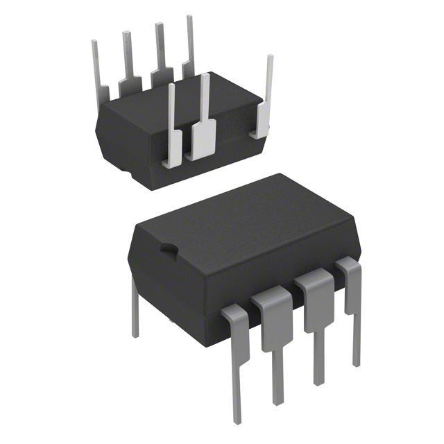
DIP8 TO-220F-7L (LF 3051)
TO-220F-7L (LF 3052)
TO-220F-7L (LF 3054)
Features and Benefits
• DIP8 package (LC551xD/LC552xD) and TO-220F-7L package (LC552xF) • Integrated on-width control circuit (it realizes high power factor by average current control) • Integrated startup circuit (no external startup circuit necessary) • Integrated soft-start circuit (reduces power stress during start-up on the incorporated power MOSFET and output rectifier) • Integrated bias assist circuit (improves the startup performance, suppresses VCC voltage droop during operation, allows reduction of VCC capacitor value as well as use of a ceramic capacitor) • Integrated Leading Edge Blanking (LEB) circuit • Integrated maximum on-width limit circuit
Figure 1. The LC5500 series packages for lower wattage versions are fully molded DIP8s, with pin 7 removed for greater isolation. For higher wattages, the TO-220F-7L fully molded package is provided, with three leadform options, all which provide a separation between pins 1 and 2.
• Dual-chip structure, with an avalanche-guaranteed power MOSFET (allows simplified surge suppressing circuits) • Protection features: ▫ Overcurrent protection (OCP): pulse-by-pulse ▫ Overvoltage protection (OVP): auto restart, OVPactivating pins vary by product series:
OVP-Activating Pins Series LC551xD LC552xD LC552xF VCC × × × ISENSE × – – OVP – × × OCP × × ×
▫ Overload protection (OLP): auto restart ▫ Thermal shutdown (TSD): halts switching operation and latches in the off-state
Part Number Assignment
The product lineup for the LC5500 series provides the following options: Part Number LC5511D LC5513D LC5521D LC5523D LC5523F LC5525F 650 MOSFET VDSS(min) (V) RDS(on) (max) (Ω) 3.95 1.9 3.95 1.9 1.1 Isolated TO-220F7L POUT* (W) 230 VAC Nonisolated DIP8 13 20 13 20 60 80 Universal (Wide) 10 16 10 16 40 55
Isolation
Package
LC55nna
A
A B C D Product series name
BC D
Indicates non-isolated or isolated: 1 – Non-isolated, 2 – Isolated On-resistance of the incorporated MOSFET: 1 – 3.95 Ω, 3 – 1.9 Ω, 5 – 1.1 Ω Indicates the package: D – DIP8, F – TO-220F-7L
*Based on the thermal rating; the allowable maximum output power can be up to 120% to 140% of this value. However, maximum output power may be limited in an applications with low output voltage or short duty cycle.
LC5500-AN, Rev.1.2
SANKEN ELECTRIC CO., LTD.
�Table of Contents
General Specifications
Block Diagrams and Pin Descriptions Package Drawings Electrical Characteristics Application Circuit Examples
1 3 5 9 15 17 17 19 21 21 22 25 26 30 32 33 33 35 35 35 35 35 37
Operation Description
On-Width Control Operation Startup Operation Operation Modes at Startup Soft-Start Function Quasi-Resonant Operation and Bottom-On Timing Latch Function Overvoltage Protection (OVP) Overload Protection (OLP) Overcurrent Protection (OCP) Input Compensation Function for Overcurrent Protection OCP Threshold Voltage with and without the OCP Input Compensation Circuit Thermal Shutdown Protection Maximum On-Width Limiting Function
Design Considerations
Peripheral Components Transformer Design Trace and Component Layout Design
LC5500-AN, Rev.1.2
SANKEN ELECTRIC CO., LTD.
2
�Block Diagrams and Pin Descriptions
This section provides block diagrams and pin descriptions of: • LC551xD for non-isolated DIP8 designs • LC552xD for isolated DIP8 designs • LC552xF for isolated TO-220-7L designs
VCC ② Controller Chip START UP TSD UVLO Reg Bias OVP S RQ OCP ③ Bottom Detection NF ⑤ OCP LEB Feedback Control Reg ④ COMP OSC OLP OTA ⑥ ISENSE Drv ① S/GND ⑧ D/ST
Figure 2. LC551xD series functional block diagram (for non-isolated DIP8 designs)
LC551xD Series Terminal List Table
Number Name S/GND VCC OCP COMP NF ISENSE – D/ST Function MOSFET source and GND terminal for the Controller chip Supply voltage input and Overvoltage protection (OVP) signal input Overcurrent Protection, quasi-resonant signal input terminal, and Overvoltage Protection (OVP) signal input Feedback phase-compensation input No function; must be externally connected to S/GND pin with as short a trace as possible, for stable operation of the IC Output current sensing voltage input and Overvoltage Protection (OVP) signal input Pin removed MOSFET drain terminal and input of the startup current
Pin-out Diagram (LC551xD)
S/GND 1 VCC 2 OCP 3 COMP 4 6 ISENSE 5 NF 8 D/ST
1 2 3 4 5 6 7 8
LC5500-AN, Rev.1.2
SANKEN ELECTRIC CO., LTD.
3
�VCC ② Controller Chip STARTUP TSD UVLO Reg Bias OVP ⑥ OVP S RQ OCP ③ Bottom Detection NF ⑤ OCP LEB Feedback Control Reg ④ FB OSC OLP Drv ① S/GND ⑧ D/ST
Figure 3. LC552xD series functional block diagram (for isolated DIP8 designs)
Pin-out Diagram (LC552xD)
S/GND 1 VCC 2 OCP 3 FB 4 8 D/ST 7 6 OVP 5 NF
LC552xD Series Terminal List Table
Number 1 2 3 4 5 6 7 Name S/GND VCC OCP FB NF OVP – D/ST
VCC ④ Controller Chip STARTUP TSD UVLO Reg Drv Bias OVP ⑦ OVP S RQ OCP ⑤ ② S/GND ① D/ST
Function MOSFET source and GND terminal for the Controller chip Supply voltage input and Overvoltage protection (OVP) signal input Overcurrent Protection, quasi-resonant signal input terminal, and Overvoltage Protection (OVP) signal input Feedback signal input and Overload Protection (OLP) signal input No function; must be externally connected to S/GND pin with as short a trace as possible, for stable operation of the IC Overvoltage Protection (OVP) signal input Pin removed MOSFET drain terminal and input of the startup current
Pin-out Diagrams (LC552xF)
D/ST S/GND NC VCC OCP FB OVP 6 7 1 2 3 4 5
8
(LF 3051)
Bottom Detection
OSC
OLP
D/ST S/GND NC VCC OCP FB OVP 6 4
1 2 3 5 7
OCP
LEB Feedback Control ⑥ FB
Reg
(LF 3052)
Figure 4. LC552xF series functional block diagram (for isolated TO-220F-7L designs)
LC552xF Series Terminal List Table
Number 1
D/ST S/GND NC VCC OCP FB OVP
Name D/ST S/GND NC VCC OCP FB OVP
Function MOSFET drain terminal and input of the startup current MOSFET source and GND terminal for the Controller chip No connection Supply voltage input and Overvoltage protection (OVP) signal input Overcurrent Protection, quasi-resonant signal input terminal, and Overvoltage Protection (OVP) signal input Feedback signal input and Overload Protection (OLP) signal input Overvoltage Protection (OVP) signal input
1 2 3 4 5 6 7
2 3 (LF 3054) 4 5 6 7
LC5500-AN, Rev.1.2
SANKEN ELECTRIC CO., LTD.
4
�Package Drawings
This section provides dimensioned drawings of the DIP8 and the TO-220-7L packages.
9.4 ±0.3 8 5
b c
1.0 +0.3 -0.05
1
4
+0.3 1.52 -0.05 (7.6 TYP)
3.4 ±0.1
7.5 ±0.5
3.3 ±0.2
4.2 ±0.3
6.5 ±0.2
0.2 5 + 0. 1 - 0.0 5
LC
a
2.54 TYP 0.89 TYP 0.5 ±0.1
Unit mm : Leadframe Material Cu : Pin treatment: Solder plating Weight Approximately 0.51g :
0~15° 0~15°
Pb-free. Device composition compliant with the RoHS directive.
Figure 5. DIP8 package drawing
a: Part #: 55xx b: Lot number 3 digits, plus D st 1 letter: Last digit of year nd 2 letter: Month Jan to September: Numeric October: O November: N December: D rd 3 letter: Week Date 1 to 10: 1 Date 11 to 20: 2 Date 21 to 31: 3 c: Internal use control number
LC5500-AN, Rev.1.2
SANKEN ELECTRIC CO., LTD.
5
�Leadform 3051
2.8 +0.2
10 ±0.2 Gate burr
4.2 ±0.2 2.6 ±0.2 Ø3.2 ±0.2 (1.1) 2.6 ±0.1 (At base of pin) 5±0.5 R-end 5.08±0.6 2.54±0.6 (At tip of pin) (At tip of pin) 0.5 0.5 0.5 Side view
(5.6)
LC
a b
15 ±0.3
7-0.62 ±0.15 10.4 ±0.5 +0.2 7-0.55 -0.1 R-end
2 ±0.15
5×P1.17±0.15 =5.85±0.15 (At base of pin) 2 1 3 4 5 6 7
+0.2 0.45 -0.1
0.5
Front view
Unit: mm Package: TO-220F-7L
Leadframe material: Cu Pin treatment: Solder dip Weight: Approximately 1.45 g Note: "Gate Burr" shows area where 0.3 mm (max) gate burr may be present.
Pin treatment Pb-free. Device composition compliant with the RoHS directive.
Figure 6. TO-220F-7L (Sanken leadform number 3051) package drawing
5±0.5
a: Part # 55xxF b: Lot number st 1 letter: Last digit of year nd 2 letter: Month Jan to September: Numeric October: O November: N December: D rd th 3 and 4 letter: Date 01 to 31: Numeric th 5 letter: Internal use control number
LC5500-AN, Rev.1.2
SANKEN ELECTRIC CO., LTD.
6
�Leadform 3052
2.8 +0.2
10 ±0.2 Gate burr
4.2 ±0.2 2.6 ±0.2 Ø3.2 ±0.2 (1.1) 2.6 ±0.1 (At base of pin) 0.5
(5.6)
LC
a b
15 ±0.3
7-0.62 ±0.15 10.4 ±0.5 +0.2 7-0.55 -0.1
R-end
2 ±0.15
5×P1.17±0.15 =5.85±0.15
0.45 +0.2 -0.1 5.08±0.6 (At tip of pin)
(At base of pin)
0.5
5±0.5 0.5
0.5
Front View 1 234567
Side View
Unit: mm Package: TO-220F-7L
Leadframe material: Cu Pin treatment: Solder dip Weight: Approximately 1.45 g Note: "Gate Burr" shows area where 0.3 mm (max) gate burr may be present.
a: Part # 55xxF b: Lot number st 1 letter: Last digit of year nd 2 letter: Month Jan to September: Numeric October: O November: N December: D rd th 3 and 4 letter: Date 01 to 31: Numeric th 5 letter: Internal use control number
Pin treatment Pb-free. Device composition compliant with the RoHS directive.
Figure 7. TO-220F-7L (Sanken leadform number 3052) package drawing
LC5500-AN, Rev.1.2
SANKEN ELECTRIC CO., LTD.
7
�Leadform 3054
2.8 ±0.2
Gate burr
2.6 ±0.2
(5.6)
15 ±0.3
LC
2.8 ±0.5 (At tip of pin) 2.5 ±0.5
a b
3-( R1)
(At base of pin)
7-0.62 ±0.15 7-0.55 +0.2 -0.1 5×P 1.17 ±0.15 = 5.85 ±0.15 (At base of pin) 5 ±0.5
+0.2 0.45 -0.1
2 ±0.15
(At tip of pin)
3.8±0.5
0.5
0.5
0.5
0.5
Plan View 1 23456 7
Side View
Unit: mm Package: TO-220F-7L
Leadframe material: Cu Pin treatment: Solder dip Weight: Approximately 1.45 g Note: "Gate Burr" shows area where 0.3 mm (max) gate burr may be present.
a: Part # 55xxF b: Lot number st 1 letter: Last digit of year nd 2 letter: Month Jan to September: Numeric October: O November: N December: D rd th 3 and 4 letter: Date 01 to 31: Numeric th 5 letter: Internal use control number
Pin treatment Pb-free. Device composition compliant with the RoHS directive.
Figure 8. TO-220F-7L (Sanken leadform number 3054) package drawing
Ø3.2 ±0.2 (1.1) 2.6 ±0.1
10 ±0.2
4.2±0.2
LC5500-AN, Rev.1.2
SANKEN ELECTRIC CO., LTD.
8
�Electrical Characteristics
This section provides separate sets of electrical characteristic data, using representative examples (refer to individual datasheets for more details): • LC551xD series (non-isolated): LC5513D is the example • LC552xD series (isolated): LC5521D is the example • LC552xF series (isolated): LC5523F is the example Current direction is sink is positive (+) and source is negative (–) in reference to the IC. LC5513D Absolute Maximum Ratings TA = 25°C, unless otherwise specified
Characteristic Drain Current1 Single Pulse Avalanche Energy1 Supply Voltage for Controller Chip OCP Pin Voltage COMP Pin Voltage ISENSE Pin Voltage Allowable Power Dissipation of MOSFET2 Operating Ambient Temperature Storage Temperature Channel Temperature
1Refer 2Mounted
Symbol IDPeak EAS VCC VOCP VCOMP VISEN PD1 TOP Tstg Tch Single pulse
Notes ILPeak = 2.7 A, VDD = 99 V, L = 20 mH
Pins 8–1 8–1 2–1 3–1 4–1 6–1 8–1 ― ― ―
Rating 4.0 86 35 −2.0 to 5.0 −0.3 to 7.0 −0.3 to 5.0 0.97 −55 to 125 −55 to 125 150
Unit A mJ V V V V W °C °C °C
to each individual product datasheet for details. on a 15 mm × 15 mm PCB.
LC5513D ELECTRICAL CHARACTERISTICS (MOSFET) TA = 25°C, unless otherwise specified
Characteristic Drain-to-Source Breakdown Voltage1 Drain Leakage Current On Resistance1 Switching
1Refer 2The
Symbol VDSS IDSS RDS(on) tf Rθch-c
Test Conditions
Pins 8–1 8–1 8–1 8–1
Min. 650 ― ― ― ―
Typ. ― ― ― ― ―
Max. ― 300 1.9 400 35.5
Unit V μA Ω ns °C/W
Time1
Thermal Resistance1,2
Between channel and case
―
to each individual product datasheet for details. thermal resistance between the channels of the MOSFET and the case. TC measured at the center of the case top surface.
LC5500-AN, Rev.1.2
SANKEN ELECTRIC CO., LTD.
9
�LC5513D ELECTRICAL CHARACTERISTICS (Controller Chip) TA = 25°C, VCC = 20 V, unless otherwise specified
Characteristic Startup Operation Operation Start Voltage Operation Stop Voltage* Operating Current Startup Circuit Operation Voltage Startup Current Startup Current Threshold Biasing Voltage-1* Startup Current Threshold Biasing Voltage-2 Normal Operation PWM Operation Frequency Maximum On-Width COMP Pin Control Voltage Lower Limit Error Amplifier Reference Voltage Error Amplifier Source Current Error Amplifier Sink Current Leading Edge Blanking Time Quasi-Resonant Operation Threshold Voltage-1 Quasi-Resonant Operation Threshold Voltage-2 Protection Operation OCP Pin Overcurrent Protection (OCP) Threshold Voltage OCP Pin Source Current OCP Pin Overvoltage Protection (OVP) Threshold Voltage Overload Protection (OLP) Threshold Voltage-1 Overload Protection (OLP) Threshold Voltage-2 ISENSE Pin OVP Threshold Voltage VCC Pin OVP Threshold Voltage Thermal Shutdown Activating Temperature *VCC(BIAS)1 > VCC(OFF) always. VOCP IOCP VBD(OVP) VCOMP(OLP)1 VCOMP(OLP)2 VISEN(OVP) VCC(OVP) TJ(TSD) 3–1 3–1 3–1 4–1 4–1 6–1 2–1 – −0.54 −120 2.2 5.0 4.1 1.6 28.5 135 −0.60 −40 2.6 5.5 4.5 2.0 31.5 – −0.66 −10 3.0 6.0 4.9 2.4 34.0 – V μA V V V V V °C fOSC tON(MAX) VCOMP(MIN) VSEN(th) ISEN(SOURCE) ISEN(SINK) tON(LEB) VBD(TH1) VBD(TH2) 8–1 8–1 4–1 6–1 4–1 4–1 3–1 3–1 3–1 11.0 30.0 0.55 0.27 −11 3 − 0.14 0.12 14.0 40.0 0.90 0.30 −7 7 500 0.24 0.17 18.0 50.0 1.25 0.33 −3 11 − 0.34 0.22 kHz μs V V μA μA ns V V VCC(ON) VCC(OFF) ICC(ON) VSTARTUP ICC(STARTUP) VCC = 13 V VCC(BIAS)1 VCC(BIAS)2 2–1 2–1 2–1 8–1 2–1 2–1 2–1 13.8 8.4 – 42 −5.5 9.5 14.4 15.1 9.4 – 57 −3.0 11.0 16.6 17.3 10.7 3.7 72 −1.0 12.5 18.8 V V mA V mA V V Symbol Test Conditions Pins Min. Typ. Max. Unit
LC5500-AN, Rev.1.2
SANKEN ELECTRIC CO., LTD.
10
�LC5521D Absolute Maximum Ratings TA = 25°C, unless otherwise specified
Characteristic Drain Current1 Single Pulse Avalanche OCP Pin Voltage FB Pin Voltage OVP Pin Voltage Allowable Power Dissipation of MOSFET2 Operating Ambient Temperature Storage Temperature Channel Temperature
1Refer
Symbol IDPeak Single pulse EAS VCC VOCP VFB VOVP PD1 TOP Tstg Tch
Notes ILPeak = 2.0 A, VDD = 99 V, L = 20 mH
Pins 8–1 8–1 2–1 3–1 4–1 6–1 8–1 ― ― ―
Rating 2.5 47 35 −2.0 to 5.0 −0.3 to 7.0 −0.3 to 5.0 0.97 −55 to 125 −55 to 125 150
Unit A mJ V V V V W °C °C °C
Energy1
Supply Voltage for Controller Chip
to each individual product datasheet for details. 2Mounted on a 15 mm × 15 mm PCB.
LC5521D ELECTRICAL CHARACTERISTICS (MOSFET) TA = 25°C, unless otherwise specified
Characteristic Drain-to-Source Breakdown Voltage1 Drain Leakage Current On Resistance1 Switching Time1 Thermal Resistance1,2
1Refer
Symbol VDSS IDSS RDS(on) tf Rθch-c
Test Conditions
Pins 8–1 8–1 8–1 8–1
Min. 650 ― ― ― ―
Typ. ― ― ― ― ―
Max. ― 300 3.95 250 42
Unit V μA Ω ns °C/W
Between channel and case
―
to each individual product datasheet for details. 2The thermal resistance between the channels of the MOSFET and the case. T measured at the center of the case top surface. C
LC5500-AN, Rev.1.2
SANKEN ELECTRIC CO., LTD.
11
�LC5521D ELECTRICAL CHARACTERISTICS (Controller Chip) TA = 25°C, VCC = 20 V, unless otherwise specified
Characteristic Startup Operation Operation Start Voltage Operation Stop Voltage* Operating Current Startup Circuit Operation Voltage Startup Current Startup Current Threshold Biasing Voltage-1* Startup Current Threshold Biasing Voltage-2 Normal Operation PWM Operation Frequency Maximum On-Width FB Pin Voltage Minimum Limit Maximum Feedback Current Leading Edge Blanking Time Quasi-Resonant Operation Threshold Voltage-1 Quasi-Resonant Operation Threshold Voltage-2 Protection Operation OCP Pin Overcurrent Protection (OCP) Threshold Voltage OCP Pin Source Current OCP Pin Overvoltage Protection (OVP) Threshold Voltage Overload Protection (OLP) Threshold Voltage-1 Overload Protection (OLP) Threshold Voltage-2 OVP Pin OVP Threshold Voltage VCC Pin OVP Threshold Voltage Thermal Shutdown Activating Temperature
*V CC(BIAS)1
Symbol VCC(ON) VCC(OFF) ICC(ON) VSTARTUP
Test Conditions
Pins 2–1 2–1 2–1 8–1 2–1 2–1 2–1
Min. 13.8 8.4 – 42 −5.5 9.5 14.4
Typ. 15.1 9.4 – 57 −3.0 11.0 16.6
Max. 17.3 10.7 3.7 72 −1.0 12.5 18.8
Unit V V mA V mA V V
ICC(STARTUP) VCC= 13 V VCC(BIAS)1 VCC(BIAS)2
fOSC tON(MAX) VFB(MIN) IFB(MAX) tON(LEB) VBD(TH1) VBD(TH2)
8–1 8–1 4–1 4–1 3–1 3–1 3–1
11.0 30.0 0.55 −10 − 0.14 0.12
14.0 40.0 0.90 −25 500 0.24 0.17
18.0 50.0 1.25 −40 − 0.34 0.22
kHz μs V μA ns V V
VOCP IOCP VBD(OVP) VFB(OLP)1 VFB(OLP)2 VOVP(OVP) VCC(OVP) TJ(TSD)
3–1 3–1 3–1 4–1 4–1 6–1 2–1 –
−0.54 −120 2.2 5.0 4.1 1.6 28.5 135
−0.60 −40 2.6 5.5 4.5 2.0 31.5 –
−0.66 −10 3.0 6.0 4.9 2.4 34.0 –
V μA V V V V V °C
> VCC(OFF) always.
LC5500-AN, Rev.1.2
SANKEN ELECTRIC CO., LTD.
12
�LC5523F Absolute Maximum Ratings TA = 25°C, unless otherwise specified
Characteristic Drain Current* Single Pulse Avalanche Energy* Supply Voltage for Controller Chip OCP Pin Voltage FB Pin Voltage OVP Pin Voltage Allowable Power Dissipation of MOSFET* Internal Frame Temperature in Operation Operating Ambient Temperature Storage Temperature Channel Temperature Symbol IDPeak EAS VCC VOCP VFB VOVP PD1 TF TOP Tstg Tch With infinite heatsink Without heatsink Single pulse ILPeak = 2.9 A, VDD = 99 V, L = 20 mH Notes Pins 1–2 1–2 4–2 5–2 6–2 7–2 1–2 1–2 ― ― ― ― Rating 9.2 99 35 −2.0 to 5.0 −0.3 to 7.0 −0.3 to 5.0 20.2 1.8 −20 to 115 −55 to 115 −55 to 125 150 Unit A mJ V V V V W W °C °C °C °C
*Refer to each individual product datasheet for details.
LC5523F ELECTRICAL CHARACTERISTICS (MOSFET) TA = 25°C, unless otherwise specified
Characteristic Drain-to-Source Breakdown Voltage1 Drain Leakage Current On Resistance1 Switching Time1 Thermal Resistance1,2
1Refer
Symbol VDSS IDSS RDS(on) tf Rθch-F
Test Conditions
Pins 1–2 1–2 1–2 1–2
Min. 650 ― ― ― ―
Typ. ― ― ― ― ―
Max. ― 300 1.9 400 3.1
Unit V μA Ω ns °C/W
Between channel and internal frame
―
to each individual product datasheet for details. 2The thermal resistance between the channels of the MOSFET and the case. T measured at the center of the case top surface. C
LC5500-AN, Rev.1.2
SANKEN ELECTRIC CO., LTD.
13
�LC5523F ELECTRICAL CHARACTERISTICS (Controller Chip) TA = 25°C, VCC = 20 V, unless otherwise specified
Characteristic Startup Operation Operation Start Voltage Operation Stop Voltage* Operating Current Startup Circuit Operation Voltage Startup Current Startup Current Threshold Biasing Voltage-1* Startup Current Threshold Biasing Voltage-2 Normal Operation PWM Operation Frequency Maximum On-Width FB Pin Voltage Minimum Limit Maximum Feedback Current Leading Edge Blanking Time Quasi-Resonant Operation Threshold Voltage-1 Quasi-Resonant Operation Threshold Voltage-2 Protection Operation OCP Pin Overcurrent Protection (OCP) Threshold Voltage OCP Pin Source Current OCP Pin Overvoltage Protection (OVP) Threshold Voltage Overload Protection (OLP) Threshold Voltage-1 Overload Protection (OLP) Threshold Voltage-2 OVP Pin OVP Threshold Voltage VCC Pin OVP Threshold Voltage Thermal Shutdown Activating Temperature *VCC(BIAS)1 > VCC(OFF) always. VOCP IOCP VBD(OVP) VFB(OLP)1 VFB(OLP)2 VOVP(OVP) VCC(OVP) TJ(TSD) 5–2 5–2 5–2 6–2 6–2 7–2 4–2 – −0.54 −120 2.2 5.0 4.1 1.6 28.5 135 −0.60 −40 2.6 5.5 4.5 2.0 31.5 – −0.66 −10 3.0 6.0 4.9 2.4 34.0 – V μA V V V V V °C fOSC tON(MAX) VFB(MIN) IFB(MAX) tON(LEB) VBD(TH1) VBD(TH2) 1–2 1–2 6–2 6–2 5–2 5–2 5–2 11.0 30.0 0.55 −10 – 0.14 0.12 14.0 40.0 0.90 −25 500 0.24 0.17 18.0 50.0 1.25 −40 – 0.34 0.22 kHz μs V μA ns V V VCC(ON) VCC(OFF) ICC(ON) VSTARTUP ICC(STARTUP) VCC = 13 V VCC(BIAS)1 VCC(BIAS)2 4–2 4–2 4–2 1–2 4–2 4–2 4–2 13.8 8.4 – 42 −5.5 9.5 14.4 15.1 9.4 – 57 −3.0 11.0 16.6 17.3 10.7 3.7 72 −1.0 12.5 18.8 V V mA V mA V V Symbol Test Conditions Pins Min. Typ. Max. Unit
LC5500-AN, Rev.1.2
SANKEN ELECTRIC CO., LTD.
14
�Application Circuit Examples
This section provides typical application circuits, using representative examples (refer to individual datasheets for more details): • LC551xD series (non-isolated) • LC552xD series (isolated) • LC552xF series (isolated)
F1
L1 D1 D2 D4 C2 D9 U1 LC551x D 8 D/ST 4 COMP Controller Chip D6 S/GND VCC OCP ISENSE 1 2 3 6 R4 D5 5 NC S/GND C4 R1 L2 C8 T1
C11
VAC
C1 D3 R5
D8 DZ1 C9 C10
R6
LED
R7
R8
C12
C3
C5 R2 (Rocp) R3 D7
C6 C7
Figure 9. Non-isolated application circuit example, with LC551xD series device
F1
L1 D1 D2 L2 T1
C11
VAC
C1 D3 D4 C2 C8 R5
D8 PC2 C9 C10
R8 R10 Q1 PC1 R12
D9 U1 LC552xD 8 D/ST C3 Controller Chip S/GND VCC OCP FB 1 2 3 4 R7 C5 R2 (Rocp) R3 C6 D7 PC1 C7 OVP 6 D5 5 NC S/GND C4 DZ2 PC2 R6 D6 C17 DZ1 C12 U2 R1 R9
R13 R11 C13 R17 + C14 R16 R14 R15 R18 C15 R19 R20
LED
C16
R4
Figure 10. Isolated application circuit example, with LC552xD series device
LC5500-AN, Rev.1.2
SANKEN ELECTRIC CO., LTD.
15
�F1
L1 D1 D2 D4 C2 C9 D9 U1 LC552xF Vcc D5 C4 Controller Chip PC2 R6 D6 C17 R1 L2 C8 R5 T1
C11
VA C
C1 D3 D8 PC2 C10 R9 R8
R10 Q1 PC1 R12 DZ2 DZ1 C12 U2 LED R14 R15 R18 C15 R19 R20 R16 C16
R13 R11 C13 R17 + C14
D/ST S/GND NC VCC OCP FB OVP 1 2 34 5 6 7 C3 C5 R2 (Rocp) R3 C6 D7 R7 PC1 C7 R4
Figure 11. Isolated application circuit example, with LC552xF series device
LC5500-AN, Rev.1.2
SANKEN ELECTRIC CO., LTD.
16
�Operation Description
All of the parameter values used in these descriptions are typical values, unless they are specified as minimum or maximum. This section describes IC operations as it is used for LED lighting power supply applications. About current direction, "+" indicates sink current toward the IC and "–" indicates source current from the IC. The pin numbers parenthesized represent LC552xF numbers.
LC551xD S/GND 1 R OCP R3
ISE NSE COMP OCP 3 D7
6 4 C6
On-Width Control Operation
LC551xD series (non-isolated designs) Figure 12 shows the
peripheral circuit at the COMP pin of the LC551xD, and figure 13 shows the on-width control. The output control is done by voltage mode control, which controls on-width depending on output load, and average current control. As showed in figure 13, in the average current control operation, the output current detection resistor voltage is compared against the reference voltage by the OTA circuit, and its output is averaged at COMP pin. This voltage is compared against the internal oscillator (OSC) by the FB comparator in order to control the on-width for the average current control operation. Here, OSC indicates the oscillator circuit, which controls the PWM operation frequency, quasi-resonant oscillation, and the maximum on-width limit. For the LC551xD devices, the recommended value of C6, which is connected to the COMP terminal, is approximately 2.2 μF. The constant output current control of the output is done as below: • When the output load current becomes less than the target value, the ISENSE pin voltage becomes low. This causes the averaged OTA circuit output voltage at the COMP pin to become high, which increases the on-width and the output current. • When the output current becomes greater than the target value, the circuits operate in the opposite way. The averaged voltage at the COMP pin becomes low, and reductions result in the on-width and the output current. Figure 14 shows the average input current waveform. The averaged COMP pin voltage becomes constant, and the duty cycle control becomes based on the EIN voltage (C2 voltage in figure 9). It makes an averaged input current sine waveform which realizes a high power factor.
LC552xD and LC552xF series (isolated designs) Figure 15
Figure 12. COMP pin peripheral circuit
LC551xD OSC
– + 4
COMP pin voltage
FB
COMP S/GND
– + 1
Current detection resistor
LED
Gate on-width
OTA
ISENSE 6
OSC
VCOMP
Gate on-width
Drain current
Figure 13. On-width control, LC551xD series
shows the peripheral circuit at the FB pin of the LC552xD/ LC552xF, and figure 16 shows the on-width control. The output
LC5500-AN, Rev.1.2
SANKEN ELECTRIC CO., LTD.
17
�COMP pin voltage
S/GND EIN Drain current Averaged input current
Figure 14. Averaged input current waveform, LC551xD series
control is done by voltage mode control, which controls on-width depending on output load, and average current control. As showed in figure 16, in the average current control operation, the output current detection resistor voltage is compared by the operational amplifier, and its output is sent to the FB pin in conjunction with the opto-coupler and averaged at the FB pin. The FB pin voltage is compared against the internal oscillator (OSC) by the FB comparator in order to control the on-width for averaged current control operation. Here, OSC indicates the oscillator circuit, which controls the PWM operation frequency, quasiresonant oscillation, and the maximum on-width limit. For the LC552xD and LC552xF series devices, the recommended value of C6, which is connected to the FB pin, is approximately 2.2 μF. The constant output current control of the output is done as below. • When the output load current becomes less than the target value, the secondary current detection resistor voltage becomes low and it results in low feedback current from the opto-coupler. It causes the averaged voltage at the FB pin to become high, and results in increases of the on-width and the output current. • When the output current becomes more than the target value, the circuits operate in the opposite way The averaged voltage at the FB pin becomes low, which reduces the on-width and the output current. Figure 17 shows the average input current waveform. The averaged FB pin voltage becomes constant, and the duty cycle control becomes based on the EIN voltage (C2 voltage in figures 10 and 11). It makes an averaged input current sine waveform which realizes a high power factor.
LC552xD (LC552xF) S/GND 1(2) R OCP R3 OCP 3(5)
FB
4(6) R7 C6
PC1
D7
Figure 15. FB pin peripheral circuit
LC552xD (LC552xF) OSC
– + 4(6)
FB pin voltage FB C6 R7 LED
Gate on-time
S/GND
PC
– +
1(2)
Current detection resistor
OSC
VFB
Gate on-time
Drain current
Figure 16. On-width control, LC552xD and LC552xF series
LC5500-AN, Rev.1.2
SANKEN ELECTRIC CO., LTD.
18
�FB pin voltage
S/GND EIN Drain current Averaged input current
Figure 17. Averaged input current waveform, LC552xD and LC552xF series
Startup Operation
Figure 18 shows the VCC pin peripheral circuit. The integrated startup circuit is connected to the D/ST pin, and it generates a constant current, ICC(STARTUP) = –3.0 mA, to charge capacitor C4 at the VCC pin. During this process, when VCC voltage reaches VCC(ON) = 15.1 V, the IC starts operation, and when its voltage exceeds VCC(BIAS)2 = 16.6 V, the startup circuit stops, in order to eliminate its own power consumption. The startup time is determined by the C4 capacitance and is expressed by the formula below: tSTART ≈ C4 VCC(ON) – VCC(INIT) |ICC(STARTUP)| (1)
LC55xxD (LC552xF)
L2 C2 P 8(1) D/ST VCC 2(4) C4 D5 R1 VD D
where tSTART is the startup time (s), and VCC(INIT) is the VCC pin initial voltage (V). A ceramic or film capacitor can be used for C4, and a value of 0.22 to 22 μF is generally recommended. Figure 19 shows the relationship between VCC voltage and the operating current, ICC . When VCC voltage reaches VCC(ON) = 15.1 V, the Controller circuit operation begins and the operating current increases. After that, if VCC voltage decreases to VCC(OFF) = 9.4 V, the Undervoltage Lockout (UVLO) circuit stops Controller circuit operation, and the operation state returns to the startup phase. After the control circuit starts up, the auxiliary winding (D in figure 18) voltage, rectified by diode D5, powers the VCC pin. VCC voltage must satisfy these conditions: VCC(BIAS)1(max) = 12.5 V < VCC < VCC(OVP)(min) = 28.5 V Initially, target 20 V in a transformer design, and then optimize its winding turns in a way that VCC voltage stays within that specified range over the conceivable input voltage range and output load conditions.
LC5500-AN, Rev.1.2
S/GND 1(2)
Figure 18. VCC pin peripheral circuit
ICC
ICC(ON) (max) = 3.7mA
Startup
Stop
9.4 V VCC(OFF)
15.1 V VCC(ON)
VCC pin voltage
Figure 19. VCC versus operation current, ICC
SANKEN ELECTRIC CO., LTD.
19
�Figure 20 shows the VCC voltage behavior at the startup phase. Immediately after the controller circuit starts operation, the auxiliary winding voltage, VD , has not yet reached its design target value, which is determined by the transformer auxiliary winding turns. Therefore, as shown figure 20, VCC voltage starts decreasing after the startup circuit turns off at VCC(BIAS)2 = 16.6 V. After a while, if the VCC voltage reaches the Startup Current Threshold Biasing Voltage-1, VCC(BIAS)1 = 11.0 V, the bias assisting function is activated in order to avoid further voltage drop and VCC voltage becomes nearly constant. Thanks to this function, the C4 value can be small, which results in shortening the startup period and improving the response time of the VCC pin overvoltage protection. Figure 21 shows the positive dependency of VCC voltage on output current. This is caused by the surge voltage, which occurs on the D/ST pin at the turn-off edge of the incorporated power MOSFET. The surge voltage is coupled to the auxiliary winding and it charges-up C4 more than the design target. In order to avoid this, insert R1 in series with D5 as shown in figure 22, and choose a value for it between several ohms to several tenths of ohms. In addition, the transformer winding structure has influence on VCC fluctuation and the two items below are examples of worsening it: • Poor coupling between the primary and secondary windings (this causes high surge voltage and is seen in a design with low output voltage and high output current). • Poor coupling between the secondary winding and the auxiliary winding D (this increases the effect of the surge voltage on the auxiliary winding voltage). Against those items, the two items below are commonly used as techniques for improvement (its construction with triple insulation wires as primary winding and/or secondary winding, and without margin region): • Separate the auxiliary winding D from the primary windings P1 and P2 (figure 23(A)); P1 and P2 are two separated primary windings. • Place the auxiliary winding D within the secondary winding S1 in order to improve the coupling of those windings (figure 23(B)); S1 is the secondary output winding.
Bobbin
VCC pin voltage
VCC(BIAS)2 = 16.6 V VCC(ON) = 15.1 V VCC(BIAS)1 = 11.0 V VCC(OFF) = 9.4 V
Operation start Startup circuit off Startup successful Bias assisting Startup failure
Time
Figure 20. VCC at startup period
VCC pin voltage
Without R1
With R1
IOUT
Figure 21. VCC versus IOUT with and without resistor R1
D5 2(4) Vcc L C55xxD (LC55xxF) S/GND 1(2)
R1 D
Added
C4
Figure 22. VCC pin peripheral circuit with R1
Bobbin
Core
P1 S1 P2 S1 D
P1, P2: Primary Winding S1: Secondary Winding D: Auxiliary winding
Core
P1 S1 D S1 P2
P1, P2: Primary Winding S1: Secondary Winding D: Auxiliary winding
(A)
(B)
Figure 23. Transformer winding structures: (A) auxiliary winding apart from the primary windings, and (B) auxiliary winding within secondary winding LC5500-AN, Rev.1.2
SANKEN ELECTRIC CO., LTD.
20
�Operation Modes at Startup
Figure 24 shows the operation modes during the startup phase of the LC551xD, and figure 25 shows those for the LC552xD and LC552xF. Note that OCP pin voltage, which determines the timing of quasi-resonant operation, is in positive voltage on the OCP pin, in reference to the S/GND pin. During two periods below at startup, IC operation is set to PWM, with fOSC = 14 kHz: • While the COMP pin voltage (for LC551xD) and FB pin voltage (for LC552xD and LC552xF), in reference to S/GND, are 0 to 0.9 V (the control voltage lower limit for the COMP pin, VCOMP(MIN), and FB pin, VFB(MIN) ): During this period, on-width is fixed at the Leading Edge Blanking Time, tBW = 500 ns. • Until the quasi-resonant signal (OCP pin voltage) reaches the Quasi-Resonant Operation Threshold Voltage-1, VBD(TH1) = 0.24 V: During this period, the output voltage is low; therefore, the auxiliary winding voltage, VD , is low. Thus the quasi-resonant signal is low.
Soft-Start Period
After those startup operations the output voltage starts increasing, when the OCP pin voltage reaches VBD(TH1) = 0.24 V, the IC is switched to quasi-resonant operation (figure 26).
Soft-Start Function
The soft-start function reduces power stress on the incorporated MOSFET and secondary rectifier during the startup phase.
LC551xD series (non-isolated designs) The soft-start operation
begins when the COMP pin voltage reaches VCOMP(MIN) = 0.9 V and lasts until the output current becomes constant. During that period, the output power gradually increases. During this period, check the items below: • VCC pin voltage does not drop to the Operation Stop Voltage, VCC(OFF) • Output current reaches the target value before the overload protection (OLP) is activated by the COMP pin voltage reaching VCOMP(OLP)2 = 4.5 V
Soft-Start Period
COMP Pin Voltage
IC turn on
FB Pin Voltage
VCOMP(MIN) = 0.90 V S/GND
IC turn on
VFB (MIN) = 0.90 V
S/GND
VCC Pin Voltage
VCC (BIAS )1 = 11.0 V S/GND
Target Current
VCC Pin Voltage
VCC (BIAS )1 = 11.0 V S/GND
Target Current
Output (LED) Current, IOUT
Constant current operation GND(IOUT)
Output (LED) Current, IOUT
Constant current operation GND(IOUT)
Drain Current, ID
t ON = tBW(500 ns)
Drain Current, ID
GND(ID )
t ON = tBW(500 ns)
GND(ID )
PWM Duration
(QR)
PWM Duration
(QR)
Figure 24. Soft-start operation waveforms at startup (LC551xD)
Figure 25. Soft-start operation waveforms at startup (LC552xD/ LC552xF)
PWM operation Quasi-resonant operation (QR) OCP Pin Voltage Drain Current, ID
Figure 26. OCP Pin Voltage (with time scale expanded)
VBD(TH1) S/GND
GND(ID)
LC5500-AN, Rev.1.2
SANKEN ELECTRIC CO., LTD.
21
�LC552xD/LC552xF series (isolated designs) The soft-start oper-
ation begins when the FB pin voltage reaches VFB(MIN) = 0.9 V and lasts until the output current becomes constant. During that period, the output power gradually increases. During this period, check the items below: • VCC pin voltage does not drop to the Operation Stop Voltage, VCC(OFF) • Output current reaches the target value before the overload protection (OLP) is activated by the FB pin voltage reaching VFB(OLP)2 = 4.5 V
t ONDLY
Ef Bottom Point EIN
Quasi-Resonant Operation and Bottom-On Timing
Figure 27 shows a basic circuit diagram of a flyback converter, in which the energy of the transformer is transferred to the secondary side after the primary side MOSFET turns off. When the primary side MOSFET keeps turning off after the energy is transferred to the secondary, the MOSFET drain node begins free oscillation based on the transformer LP , and CV across the drain and source pins, after the energy is completely transferred to the secondary. The quasi-resonant operation is the VDS bottom-on operation that turns on the MOSFET at the bottom point of VDS free oscillation. Because of that, switching loss and switching noise are reduced. Therefore, highly efficient and low noise converters can be realized. Figure 28 shows an ideal VDS waveform of this mode. Turning on the MOSFET at the bottom of VDS is done by creating certain duration, delay time tONDLY , as figure 28 shows from the start of VDS free oscillation. This delay time is created by exploiting the auxiliary winding voltage, which synchronizes to the drain voltage VDS waveform and it is called the quasi-resonant signal.
EIN:
VDS
I OFF
ID tON
Half cycle of free oscillation, tONDLY
≈ √ L P × CV
Figure 28. Waveforms of the ideal Bottom-On mode
Input voltage Flyback voltage
Ef ID EIN
NP LP
NS I OFF
V OUT COUT
Ef:
Ef =
NP: NS: VOUT: Vf: ID: IOFF:
NP NS
(VOUT + Vf)
(2)
Number of turns in the primary winding Number of turns in the secondary winding Output voltage Forward voltage of the secondary rectifier Drain current of the power MOSFET Current running through the secondary rectifier during the power MOSFET off-period Voltage resonant capacitor Primary inductance
CV
Figure 27. Basic flyback converter circuit
CV: LP:
LC5500-AN, Rev.1.2
SANKEN ELECTRIC CO., LTD.
22
�Figure 29 shows the OCP pin peripheral circuit. D6, R4, C7 and D7 form a delay circuit, and the auxiliary winding flyback voltage, Erev1 , is fed through the delay circuit and provides positive voltage, the quasi-resonant signal, to the OCP pin. Figure 30 shows the forward voltages versus the power supply.
T1 EIN C2 P Clamping snubber EIN EF D5 C4 Erev 1 R1
After the power MOSFET turns off, the quasi-resonant signal immediately goes up and it exceeds the Quasi-Resonant Operation Threshold Voltage-1, VBD(TH1) = 0.24 V. After this occurs, the power MOSFET remains off until the quasi-resonant signal comes down enough to cross the Quasi-Resonant Operation Threshold Voltage-2, VBD(TH2) = 0.17 V. Then the power MOSFET again turns on. In addition, at the point, the threshold voltage goes up to VBD(TH1) automatically to prevent malfunction of the quasi-resonant operation from noise interference.. During that period, C7 must cause a delay time, tONDLY , such that the power MOSFET turns on at the bottom point of VDS ; so select an appropriate C7 value. R3 is recommended to be between 100 and 330 Ω, and C5 to be between 100 and 470 pF. R4 must set the range for the quasi-resonant signal: greater than or equal to VBD(TH1) under input and output conditions where VCC becomes lowest, but less than the OCP Pin Overvoltage Protection (OVP) Threshold Voltage, VOCP(OVP) = 2.6 V, under conditions where VCC becomes highest. Figure 31 defines the pulse width of the quasi-resonant signal. For initiating quasi-resonant operation, the quasi-resonant signal pulse width between the two points VBD(TH1) and VBD(TH2) , tQR, must be equal to 1.2 μs or more. This pulse width must be ensured, while at the same time the OCP pin peak voltage, VBD(PK) , is recommended to be between 1.5 and 2.0 V. Both conditions should be satisfied throughout the power supply input and output ranges, over variations in R3 and R4 actual component values.
D
C3
8(1) D/ST
2(4) V CC
D6 R4
Efw1
Forward voltage
Flyback voltage
LC5500
S/GND 1(2)
OCP 3(5)
D7 R3 C7 VBD
C5 ROCP
Figure 29. OCP pin peripheral circuit
VD
VBD(PK), 1.5 to 2.0 V recommended, but less than 2.6 V
Erev1 Auxiliary winding 0 voltage Efw1
V BD(TH1) = 0.34 V (max) V BD(TH2 ) = 0.22 V (max)
tON VBD Quasiresonant signal VBD(TH1)
0
S/GND
Pulse width, t QR ≥ 1.2 μs
VBD(TH2)
Figure 30. Auxiliary winding voltage and quasi-resonant signal
Figure 31. Definition of the pulse width of the quasi-resonant signal
LC5500-AN, Rev.1.2
SANKEN ELECTRIC CO., LTD.
23
�The formula below is used to calculate R4: R4 = R3 (VCC – VBD(PK) – 2Vf ) VBD(PK) (3)
given R3 = 220 Ω, VBD(PK) = 1.5 V, VCC = 16 V, and the Vf of D6 and D7 = 0.8 V. R4 is approximately 1.89 kΩ, and it is 1.8 kΩ in the E12 series. If the pulse width is not satisfied, increase R3 or decrease R4, in order to raise VBD(PK) . Alternatively, increasing the capacitance of resonant capacitor C3 is also effective because it widens the free oscillation period. However, it causes an additional switching loss increase; therefore, ensure the IC temperature rise is acceptable. Figure 32 shows two different OCP pin waveforms, comparing transformer coupling conditions between the primary and secondary winding. The poor coupling tends to happen in a low output voltage (small number of LEDs) transformer design with high NP / NS turns ratio (NP and NS indicate the number of turns of the primary winding and secondary winding, respectively), and it results in high leakage inductance. The poor coupling causes high surge voltage ringing at the power MOSFET drain pin when it turns off. That high surge voltage ringing is coupled to the auxiliary winding and then the inappropriate quasi-resonant signal, as in figure 32B, is created. The OCP pin has a blanking period of
250 ns (max) to avoid reacting to it, but if the surge voltage continues longer than that period, the IC responds to it and repeatedly turns the power MOSFET on and off at high frequency. This results in an increase of the MOSFET power dissipation and temperature, and it can be damaged. If this phenomenon is observed, countermeasures include: • Place C5 as close to the OCP and S/GND pins as possible • Separate the loop trace between the OCP pin and the S/GND pin from any high current trace • Loosen the transformer coupling between the auxiliary winding and primary winding • Reinforce the clamping snubber circuit to reduce the surge voltage In addition, the OCP pin waveform during operation should be measured by connecting test probes with leads to the OCP pin and the GND pin as short as possible, in order to measure any surge voltage correctly. Timing adjustment of the bottom-on is done by selecting the value of C7 (figure 29). To do so, observe the power MOSFET drain voltage, VDS , the drain current, ID , and the quasi-resonant signal. Then optimize the C7 value to adjust the delay time of tONDLY so that the MOSFET turns on at the bottom point of VDS.
VOCP(OVP) = 2.6 V VBD(TH1) = 0.24 V VBD(TH2) = 0.17 V S/GND OCP pin blanking time, 250 ns (max) (B) Inappropriate OCP Voltage, Erev2
(A) Proper OCP Voltage, Erev2
Figure 32. OCP pin waveform of a poorly coupled transformer (B)
LC5500-AN, Rev.1.2
SANKEN ELECTRIC CO., LTD.
24
�As shown in figure 33: • If the turn-on point is earlier than the bottom of the VDS signal, it causes higher switching losses. In that situation, delay the turn-on point by increasing the C7 value. • In the converse situation, if the turn-on point is later than the VDS bottom point, it also causes higher switching losses, but in that case, advance the turn-on point by decreasing the C7 value.
Latch Function
Thermal shutdown (TSD) protection is latched. When the latch circuit is activated, the IC stops switching operation, and therefore the VCC voltage declines. However, the startup circuit turns on again when VCC reaches VCC(BIAS)1 = 11.0 V, in order to avoid reaching the operation stop-
AC mains frequency (50 Hz / 60 Hz) 2 × AC mains frequency VDS (peak) VDS E IN(max) GND
Turn-on occurring before the VDS bottom point
Turn-on occurring after the VDS bottom point
Early turn-on point
Delayed turn-on point
V DS Bottom point I OFF Free oscillation, fR
V DS Bottom point I OFF Free oscillation, fR
ID t ON
VBD(TH1) VBD(TH2)
ID t ON
VBD(TH1) VBD(TH2)
VOCP
S/GND
VOCP Auxiliary Winding Voltage
S/GND
Auxiliary Winding Voltage
S/GND
S/GND
1 fR ≈ 2 √ L × C P V
Figure 33. Effects of failure to turn on precisely at the VDS bottom point: (left) turn-on too early, (right) turn-on too late
LC5500-AN, Rev.1.2
SANKEN ELECTRIC CO., LTD.
25
�ping voltage, VCC(OFF) = 9.4 V. Thus IC operation in latch mode is maintained. To release the IC from latch mode, cut off the AC mains and let VCC voltage drop below VCC(OFF).
Overvoltage Protection (OVP)
LC551xD series (non-isolated designs) The LC551xD series
operation. During this function, the bias assist function is disabled, and the VCC voltage decreases to VCC(OFF) = 9.4 V. After that, the startup circuit is activated, and the operation begins intermittent operation by repeating the restart and operation process as long as the OVP condition remains. In addition, because VCC voltage is proportional to the output voltage, it can be used to detect an output overvoltage event, such as open load condition. In this situation, the detecting voltage is expressed by the formula below: VOUT(OVP) = VOUT(normal operation) VCC(normal operation) 31.5 (V) (4)
has three OVP activation methods link to the VCC pin, to the OCP pin, and to the ISENSE pin: • VCC Pin Overvoltage Protection. figure 34 shows the waveforms of the OVP function on the VCC pin. When the VCC pin voltage with reference to the S/GND pin reaches and exceeds VCC(OVP) = 31.5 V, OVP is activated and the IC stops switching
VCC pin voltage
COMP pin voltage
Drain current, ID
Figure 34. Waveforms when VCC pin OVP is being activated (LC551xD)
LC5500-AN, Rev.1.2
SANKEN ELECTRIC CO., LTD.
26
�• OCP Pin Overvoltage Protection. Figure 35 shows the OCP pin OVP function. When the OCP pin voltage with reference to the S/GND pin reaches VOCP(OVP) = 2.6 V or more, OVP is activated. During this function, the bias assist function is disabled, and thus the IC enters intermittent operation as described in the VCC pin OVP section, above. This can be used as protection in the event that the quasi-resonant signal setup is mistaken or excess load current happens in the use of a poor coupling transformer between the primary and secondary winding.
• ISENSE Pin Overvoltage Protection. Figure 36 shows the ISENSE pin OVP operation. When the ISENSE pin voltage with reference to the S/GND pin reaches and exceeds VISEN(OVP) = 2.0 V or more, OVP is activated. During this function, the bias assist function is disabled, and thus the IC enters intermittent operation as described in the VCC pin OVP section, above. As shown in figure 9, with Zener diode DZ1 this function can be used to detect an excess output voltage, such as caused by an open load condition, and protect the circuit.
VCC pin voltage
VCC(ON)= 15.1V VCC(OFF)= 9.4V
VBD(OVP)= 2.6V OCP pin voltage
Drain current, ID
Figure 35. Waveforms when OCP pin OVP is being activated (LC551xD)
VCC pin voltage
VCC(OFF)= 9.4V
VCC(ON)= 15.1V
ISENSE pin voltage
VISEN(OVP)= 2.0V
COMP pin voltage
VCOMP(MIN)= 0.90V
Drain current, ID
tON= tON(LEB)(500ns)
Figure 36. Waveforms when ISENSE pin OVP is being activated (LC551xD)
LC5500-AN, Rev.1.2
SANKEN ELECTRIC CO., LTD.
27
�LC552xD/LC552xF series (isolated designs) The LC552xD and
LC552xF series have three OVP activation methods link to the VCC pin, to the OCP pin, and to the OVP pin: • VCC Pin Overvoltage Protection. figure 37 shows the waveforms of the OVP function. When the VCC pin voltage with reference to the S/GND pin reaches and exceeds VCC(OVP) = 31.5 V or more, OVP is activated and the IC stops switching operation.
During this function, the the bias assist function is disabled, and the VCC voltage decreases to VCC(OFF) = 9.4 V. After that, the startup circuit is activated, and the operation begins intermittent operation by repeating the restart and operation process as long as the OVP condition remains. In addition, because VCC voltage is proportional to the output voltage, it can be used to detect output overvoltage events, such as open load condition. In this situation, the detecting voltage is expressed by equation 4.
VCC(OVP)= 31.5V VCC pin voltage VCC(ON)= 15.1V VCC(OFF)= 9.4V
FB pin voltage
VFB(MIN)= 0.90V
Drain current, ID tON= tON(LEB)(500ns)
Figure 37. Waveforms when VCC pin OVP is being activated (LC552xD and LC552xF)
LC5500-AN, Rev.1.2
SANKEN ELECTRIC CO., LTD.
28
�• OCP Pin Overvoltage Protection. Figure 38 shows the OCP pin OVP function. When the OCP pin voltage with reference to the S/GND pin reaches VOCP(OVP) = 2.6 V, OVP is activated. During this function, the bias assist function is disabled, and thus the IC enters intermittent operation as described in the VCC pin OVP section, above. This can be used as protection in the event the quasi-resonant signal setup is mistaken or excess load current happens in the use of a poor coupling transformer between the primary and secondary winding.
• OVP pin Overvoltage Protection. Figure 39 shows the OVP pin OVP function. When the OVP pin voltage with reference to the S/GND pin reaches and exceeds VOVP(OVP) = 2.0 V, OVP is activated. During this function, the bias assist function is disabled, and thus the IC enters intermittent operation as described in the VCC pin OVP section, above.. As shown in figure 10 and figure 11, with PC2 this function can be used to detect high output voltage, such as an open load condition.
VCC pin voltage VCC(OFF)= 9.4V
VCC(ON)= 15.1V
VOCP(OVP)= 2.6V OCP pin voltage
Drain current, ID
Figure 38. Waveforms when OCP pin OVP is being activated (LC552xD and LC552xF)
VCC pin voltage
VCC(OFF)= 9.4V
VCC(ON)= 15.1V
OVP pin voltage
VOVP(OVP) = 2.0V
FB pin voltage
VFB(MIN)= 0.90V
Drain current, ID
tON= tON(LEB)(500ns)
Figure 39. Waveforms when OVP pin OVP is being activated (LC552xD and LC552xF)
LC5500-AN, Rev.1.2
SANKEN ELECTRIC CO., LTD.
29
�Overload Protection (OLP)
If the MOSFET drain current is limited by the overcurrent protection for a certain delay period, tDLY , Overload Protection is activated and the IC enters intermittent oscillation mode operation. This reduces the power-up stress on the incorporated power MOSFET and secondary rectifier.
LC551xD series (non-isolated designs) Figure 40 shows the
in order to avoid reaching VCC(OFF) = 9.4 V. When the ISENSE pin voltage reaches VSEN(TH) = 0.30 V, the output of the OTA circuit becomes zero, and therefore the internal constant current source at the COMP pin starts charging capacitor C6. When the COMP pin voltage reaches Overload Protection Threshold Voltage-2, VCOMP(OLP)2 = 4.5 V, the on-width is set to the Leading Edge Blanking time, tON(LEB) = 500 ns. Meanwhile, the capacitor charging is ongoing and when it reaches Overload Protection Threshold Voltage-1, VCOMP(OLP)1 = 5.5 V, the switching operation stops. At the same time, the startup circuit is activated and the operation begins intermittent operation by repeating the restart and operation stop processes as long as the overload condition remains.
peripheral circuit at the COMP pin, and figure 41 shows operation when OLP is activated. At an overload condition, the output voltage, the VCC pin voltage, and the ISENSE pin voltage drop. When the VCC pin voltage reaches VCC(BIAS) = 11.0 V, the bias assist function is enabled
Figure 40. COMP pin peripheral circuit
VCC pin voltage
VCC(OFF)= 9.4V
VCC(ON)= 15.1V VCC(BIAS)1= 11.0V
COMP pin voltage
VCOMP(OLP)1= 5.5V VCOMP(OLP)2= 4.5V VCOMP(MIN)= 0.90V
Drain current, ID
tON= tON(LEB)(500ns)
Figure 41. Waveforms when OLP is being activated (LC551xD)
LC5500-AN, Rev.1.2
SANKEN ELECTRIC CO., LTD.
30
�LC552xD/LC552xF series (isolated designs) Figure 42 shows
the peripheral circuits at the FB pin of the LC552xD/LC552xF series and figure 43 shows the waveforms when the Overload Protection (OLP) is activated. At an overload condition, the output voltage drops and it results in a feedback signal from the secondary output becoming zero. After that, the internal constant current source at the FB pin starts to charge the C6 capacitor. When the FB pin voltage reaches the Overload Protection
Threshold Voltage-2, VFB(OLP)2 = 4.5 V, the on-width is set to Leading Edge Blanking time, tON(LEB) = 500 ns. In the meanwhile, the capacitor charging is ongoing and when it reaches at Overload Protection Threshold Voltage-1, VFB(OLP)1 = 5.5 V, the switching operation stops. At the same time, the startup circuit is activated and the operation begins intermittent operation by repeating the restart and operation stop processes as long as the overload condition remains.
7VReg LC552xD (LC552x F) S/GND OCP 3(5) 1(2) ROCP FB C6 4(6) R7
Figure 42. FB pin peripheral circuit
VCC pin voltage
VCC(OFF)= 9.4V
VCC(ON)= 15.1V VCC(BIAS)1= 11.0V
FB pin voltage
VFB(OLP)1= 5.5V VFB(OLP)2= 4.5V VFB(MIN)= 0.90V
Drain current, ID
tON= tON(LEB)(500ns)
Figure 43. Waveforms when OLP is being activated (LC552xD/ LC552xF)
LC5500-AN, Rev.1.2
SANKEN ELECTRIC CO., LTD.
31
�Overcurrent Protection (OCP)
The Overcurrent Protection (OCP) feature monitors the power MOSFET drain current on a pulse-by-pulse basis, in order to limit output power. The drain current is detected by a current detection resistor, ROCP , and the voltage across it, VROCP , is fed through R3 to the OCP pin to be detected by it. When the ROCP voltage, VROCP , reaches the value of the following formulas, the power MOSFET turns off. VROCP = – |VOCP | + R3 |IOCP | (5)
C2 LC55xxD (LC55xxF) Controller Chip Logic Drive
1(2)
D/ST 8(1)
P
C3
OCP Comparator
S/GND
3(5)
where VOCP: Overcurrent Detection Threshold Voltage, -0.60 V, and IOCP: OCP Pin Source Current, -40 μA. In order to minimize effects of variation in the internal resistor, R3 (figure 44) is recommended to have a value from 100 to 330 Ω. and C5 is recommended to have a value from 100 to 470 pF, with good temperature characteristics. Selecting larger capacitances slows OCP response, and results in an increase in the drain current peak at transient conditions, such as start-up. Because the OCP function is designed for peak current detection, there is a chance that it will react to the surge current at the power MOSFET turn-on edge. In order to avoid this, the Leading Edge Blanking Time is set. The Leading Edge Blanking Time, tON(LEB) = 500 ns, is set. The surge current pulse width must be less than tON(LEB) as shown in figure 45. In case its width is longer than that, try these measures: • adjust the turn-on point to the VDS bottom point • reduce the voltage resonant capacitor CV (C3 in figure 44) capacitance • reduce the secondary rectifier snubber capacitor capacitance With the quasi-resonant converter, the peak drain current at the same output load condition becomes different in various AC input voltages (85 VAC to 265 VAC), that is, when the AC input voltage is high, the peak drain current is low because the operation frequency becomes high. When the OCP threshold voltage is fixed constant, the output current, IOUT , in an OCP operation increases according to an increase of AC input voltage, as shown in (A) IOUT without input compensation of figure 46. In the maximum AC input voltage range, in order to control output current at OCP operation, IOUT(OCP) , an external OCP input compensation circuit (DX1, DZX1, RX1) is added as shown in figure 47. For more details as to how to set it, refer to the next section, Input Compensation Function for Overcurrent Protection.
+
− 0.6V
OCP
Reg
C5 Filter R3
Rocp
VRocp
Figure 44. Minus detection OCP circuit
tON(LEB) S/GND
OCP detection period
VROCP
Surge pulse voltage width at turning on
Figure 45. OCP pin voltage, converted from MOSFET drain current by ROCP
A Output Current at OCP, IOUT(OCP)
B
IOUT target output level C
85 AC Input Voltage (V)
265
Figure 46. Input compensation OCP circuit: (A) IOUT without input compensation; (B) IOUT with appropriate input compensation; (C) with inappropriately set input compensation, more than enough amount of compensation, IOUT cannot meet target
LC5500-AN, Rev.1.2
SANKEN ELECTRIC CO., LTD.
32
�L2
Input Compensation Function for Overcurrent Protection
The auxiliary winding forward voltage Efw1 is proportional to the input voltage, EIN . Efw1 is applied to DZX1 , and RX1 and R3 translate the voltage Efw1 – Zener voltage of DZX1 , into the input Compensation Current, I. This input Compensation Current, I, creates the voltage of R3 × I, and it lowers the compensated OCP threshold voltage to less than the original OCP threshold voltage, VOCP = –0.6 V. This way, when EIN is high, the compensation amount becomes high. The DZX1 Zener diode is used to set the voltage at which the input compensation begins, so choose the Zener voltage value that is equal to Efw1 at the time when input compensation begins. Optimize the circuit in a way to minimize the difference between the overcurrent points at low and high AC input voltage. Also ensure that the output current meets its target over the entire AC input voltage range, as the normal curve shown in figure 46. The OCP pin voltage, including surge voltage, must not exceed its absolute maximum rating of –2.0 to 5.0 V at the highest AC input voltage.
ROCP
C2 8(1) D/ST C3
LC55xxD (LC55xxF)
P
D5 2(4) C4 R1
VCC
D
DX1
S/GND OCP 1(2) C5 3(5) D7 R3
D6 R4 C7 RX1
DZX1
Figure 47. Input compensation OCP circuit
EIN C2 D5 8(1) D/ST C4
P
R1
NP
S
NS
OCP Threshold Voltage with and without the OCP Input Compensation Circuit
Without the input compensation circuit, as shown in the figure 50 upper panel, the overcurrent detecting voltage is equal to the sum of the Overcurrent Protection Threshold Voltage, VOCP = −0.60 V, and the voltage across R3 from the OCP pin source current, IOCP = – 40 μA. VROCP = – |ROCP × IDP| = – |VOCP | + R3 × |IOCP | (6)
D
ND
Flyback voltage Erev1 Forward voltage Efw1
LC55xxD (LC55xxF)
ID
S/GND OCP 1(2) C5 3(5) D6 C7 D7 RX1 DX1 R4 DZX1
ROCP
IOCP
R3
Compensation Current, I
Auxiliary Winding Forward Voltage
In the converse situation, with the input compensation circuit, as shown in the figure 50 lower panel, the overcurrent detecting voltage is equal to the sum of the Overcurrent Protection Threshold Voltage, VOCP = −0.60 V, the voltage across R3 from the OCP pin source current, IOCP , and the voltage across R3 from the input Compensation Current, I : V 'ROCP= – |VOCP | + R3 ×| IOCP | – R3 × I (7)
Figure 48. OCP input compensation circuit
AC Input Voltage = 85 V AC Input Voltage = 265 V 0 Efw1
}DZX1
• Determining OCP pin input compensation circuit component values Given: EIN(PK) = C2 voltage IDP = MOSFET peak drain current VFX1 = DX1 forward voltage DZX1 = DZX1 Zener voltage
0 Efw2 OCP input compensation starting point: Efw1 ≈ DZX1
Figure 49. OCP input compensation
Time
Time
LC5500-AN, Rev.1.2
SANKEN ELECTRIC CO., LTD.
33
�1. The overcurrent detecting peak drain current, IDP(OCP) , without the input compensation circuit, is expressed by the following, based on equation 6, from figure 50, upper panel: |V | + R3 × |IOCP| IDP(OCP) = OCP (8) ROCP 2. On the other hand, the overcurrent detecting peak drain current, I'DP(OCP) , with the input compensation circuit, is expressed by the following, based on equation 7, from figure 50, lower panel: |V | + R3 × (|IOCP| – I ) I 'DP(OCP) = OCP (9) ROCP Here, I'DP is the peak drain current where the output power of the maximum AC input voltage becomes the same as that limited by OCP at the minimum AC input voltage. 3. From equations 8 and 9, the compensation current, I, of the input compensation circuit, is expressed as follows: R I = ( |I DP(OCP) | – |I 'DP(OCP)| ) × OCP R3 (10)
I=
Efw1 – DZX1 – VFX1 RX1 + R3 + ROCP
(12)
assuming: R3, ROCP


 工商网监
湘ICP备2023018690号
工商网监
湘ICP备2023018690号
