IOUT = 1 A Linear Regulator ICs
SI-3000KD Series
Data Sheet
Description
Packages
The SI-3000KD series are linear regulator ICs whose
maximum output current is 1 A. The output voltage of
the SI-3010KD is adjusted by external resistors. The
output voltage of the SI-3033KD is 3.3 V fixed.
The ICs have a built-in low saturation PNP bipolar
transistor and can operate with a low input/output
voltage difference. The ICs have various functions
including the Output On/Off Function, the Overcurrent
Protection and the Thermal Shutdown, and achieve a
linear regulator circuit with few external components.
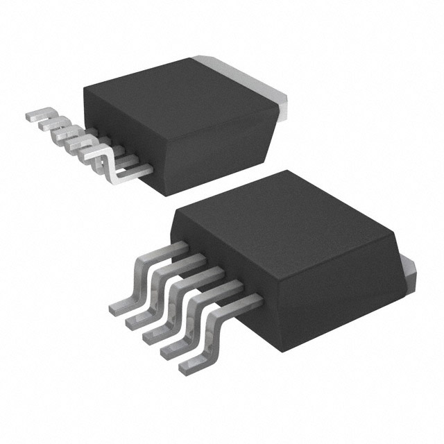
TO263-5L
Features
Not to scale
Selection Guide
Part Number
SI-3010KD
SI-3033KD
● Low Dropout Voltage, ΔVDIF ≤ 0.6 V
(IOUT = 1 A)
● Output On/Off Function
● Protections
Overcurrent Protection (OCP): Fold-back (SI3010KD), Drooping (SI-3033KD), Auto-restart
Thermal Shutdown (TSD): Auto-restart
Output Voltage
Adjustable
3.3 V
Applications
● Audio Visual Equipment
● Office Automation Equipment
● White Goods
Typical Application (SI-3010KD)
VC
VIN
GND
VO
ADJ
SI-3010KD
1
2
3
4
5
ON/OFF
VIN
D1
VOUT
R1
CIN
COUT
R2
SI-3000KD-DSE Rev.2.0
SANKEN ELECTRIC CO., LTD.
Sep. 11, 2020
https://www.sanken-ele.co.jp/en
© SANKEN ELECTRIC CO., LTD. 2013
1
�SI-3000KD Series
Contents
Description ------------------------------------------------------------------------------------------------------ 1
Contents --------------------------------------------------------------------------------------------------------- 2
1. Absolute Maximum Ratings----------------------------------------------------------------------------- 3
2. Thermal Resistance Characteristics ------------------------------------------------------------------- 3
3. Recommended Operating Range ----------------------------------------------------------------------- 4
4. Electrical Characteristics -------------------------------------------------------------------------------- 5
4.1. SI-3010KD -------------------------------------------------------------------------------------------- 5
4.2. SI-3033KD -------------------------------------------------------------------------------------------- 6
5. Performance Curves -------------------------------------------------------------------------------------- 7
5.1. SI-3010KD -------------------------------------------------------------------------------------------- 7
5.2. SI-3033KD ------------------------------------------------------------------------------------------ 10
6. Derating Curve ------------------------------------------------------------------------------------------ 12
7. Block Diagram ------------------------------------------------------------------------------------------- 13
8. Pin Configuration Definitions ------------------------------------------------------------------------- 14
9. Typical Application ------------------------------------------------------------------------------------- 15
9.1. SI-3010KD ------------------------------------------------------------------------------------------ 15
9.2. SI-3033KD ------------------------------------------------------------------------------------------ 16
10. Physical Dimensions ------------------------------------------------------------------------------------ 17
10.1. Land Pattern Example --------------------------------------------------------------------------- 17
11. Marking Diagram --------------------------------------------------------------------------------------- 18
12. Operational Description ------------------------------------------------------------------------------- 19
12.1. Constant Voltage Control------------------------------------------------------------------------ 19
12.2. Output Voltage Setting (Only SI-3010KD) --------------------------------------------------- 19
12.3. Overcurrent Protection Function (OCP) ----------------------------------------------------- 19
12.4. Thermal Shutdown (TSD) ----------------------------------------------------------------------- 19
12.5. Output On/Off Function ------------------------------------------------------------------------- 19
13. Design Notes ---------------------------------------------------------------------------------------------- 20
13.1. Considerations in Circuit Configuration (Only SI-3010KD) ----------------------------- 20
13.2. External Components ---------------------------------------------------------------------------- 20
13.3. PCB Pattern Layout ------------------------------------------------------------------------------ 20
13.4. Thermal Design ------------------------------------------------------------------------------------ 21
Important Notes ---------------------------------------------------------------------------------------------- 22
SI-3000KD-DSE Rev.2.0
SANKEN ELECTRIC CO., LTD.
Sep. 11, 2020
https://www.sanken-ele.co.jp/en
© SANKEN ELECTRIC CO., LTD. 2013
2
�SI-3000KD Series
1.
Absolute Maximum Ratings
Unless otherwise specified, TA = 25 °C.
Parameter
Symbol
Conditions
Rating
Unit
Remarks
V
SI-3010KD
17
V
SI-3033KD
35
(1)
VIN Pin Voltage
VIN
VC Pin Voltage
VC
VIN
V
Output Current
IOUT
1
A
3
W
TJ
−30 to 125
°C
TOP
−30 to 85
°C
TSTG
−30 to 125
°C
Power Dissipation
Junction Temperature
Operating Ambient Temperature
(2)
Storage Temperature
2.
Mounted on the board (2)
PD
Thermal Resistance Characteristics
Parameter
Symbol
Thermal Resistance between Junction
and Ambient
Thermal Resistance between Junction
and Case(3)
θJ-A
Conditions
Min.
Typ.
Max.
Unit
—
—
33.3
°C/W
—
—
3
°C/W
Mounted on the board (2)
θJ-C
TC
Figure 2-1.
Case Temperature Measurement Point
(1)
Limited by overvoltage protection voltage of 33 V.
Glass-epoxy board (40 mm × 40 mm), copper area 100%
(3)
The case temperature (°C) is measured at the point defined in Figure 2-1.
(2)
SI-3000KD-DSE Rev.2.0
SANKEN ELECTRIC CO., LTD.
Sep. 11, 2020
https://www.sanken-ele.co.jp/en
© SANKEN ELECTRIC CO., LTD. 2013
3
�SI-3000KD Series
3.
Recommended Operating Range
Parameter
VIN Pin Voltage
Output Current
Output Voltage
Operating Ambient Temperature
Operating Junction Temperature
(1)
(2)
Symbol
VIN
IOUT
VOUT
TOP(A)
TOP(J)
Min.
2.4(1)
(1)
0
1.1
−30
−20
Max.
27(2)
6(2)
1(2)
16
85
100
Unit
V
V
A
V
°C
°C
Remarks
SI-3010KD
SI-3033KD
SI-3010KD
Should be set to VOUT + dropout voltage or higher. See Section 4 for dropout voltage.
The following equation shows the relationship between VIN, VOUT, and IOUT. Thus, Dropout Voltage (VIN − VOUT)
and/or IOUT may be limited in some conditions.
PD = (VIN − VOUT ) × IOUT
SI-3000KD-DSE Rev.2.0
SANKEN ELECTRIC CO., LTD.
Sep. 11, 2020
https://www.sanken-ele.co.jp/en
© SANKEN ELECTRIC CO., LTD. 2013
4
�SI-3000KD Series
4.
Electrical Characteristics
4.1.
SI-3010KD
Current polarities are defined as follows: current going into the IC (sinking) is positive
out of the IC (sourcing) is negative current (−).
Unless otherwise specified, TA = 25 °C, VOUT = 5 V, R2 = 10 kΩ.
Parameter
Symbol
Conditions
Min
0.98
Reference Voltage
VREF
VIN = 7 V, IOUT = 10 mA
VIN = 6 V to 15 V,
—
Line Regulation
ΔVLINE
IOUT = 10 mA
VIN = 7 V,
—
Load Regulation
ΔVLOAD
IOUT = 0 A to 1 A
—
IOUT = 0.5 A
Dropout Voltage
ΔVDIF
—
IOUT = 1 A
Output Voltage Temperature
—
ΔVOUT/ΔTA TJ = 0 °C to 100 °C
Coefficient
VIN = 7 V,
—
Ripple Rejection Ratio
RREJ
f = 100 Hz to 120 Hz
IOUT = 0.1 A
Overcurrent Protection Operating
IS1
VIN = 7 V
1.1
Current (1)
VIN = 7 V, IOUT = 0 A,
—
Quiescent Current
IQ
VC = 2 V
Circuit Current during Regulator
—
IQ(OFF)
VIN = 7 V, VC = 0 V
Output Off
VC Pin Voltage (Output On)
VC_IH
2
—
VC Pin Voltage (Output Off)
VC_IL
—
VC Pin Current (Output On)
IC_IH
VC = 2.0 V
−5
VC Pin Current (Output Off)
IC_IL
VC = 0 V
33
Overvoltage Protection Voltage
VOVP
IOUT = 10 mA
(1)
current (+); current coming
Typ.
1.00
Max
1.02
Unit
V
—
30
mV
—
75
mV
—
—
0.3
0.6
V
V
±0.5
—
mV/°C
55
—
dB
—
—
A
—
600
μA
—
1
μA
—
—
—
0
—
—
0.8
40
—
—
V
V
μA
μA
V
After the Overcurrent Protection is activated, IS1 is measured when the output voltage, VOUT, (conditions: VIN = 7 V,
IOUT = 10 mA) decreases by 5%.
SI-3000KD-DSE Rev.2.0
SANKEN ELECTRIC CO., LTD.
Sep. 11, 2020
https://www.sanken-ele.co.jp/en
© SANKEN ELECTRIC CO., LTD. 2013
5
�SI-3000KD Series
4.2.
SI-3033KD
Current polarities are defined as follows: current going into the IC (sinking) is positive current (+); current coming
out of the IC (sourcing) is negative current (−).
Unless otherwise specified, TA = 25 °C.
Parameter
Symbol
Conditions
Min
Typ.
Max
Unit
3.234
3.300
3.366
Setting Output Voltage
VOUT
VIN = 5 V, IOUT = 10 mA
V
VIN = 5 V to 10 V,
—
—
15
Line Regulation
ΔVLINE
mV
IOUT = 10 mA
VIN = 5 V,
—
—
50
Load Regulation
ΔVLOAD
mV
IOUT = 0 A to 1 A
—
—
0.4
IOUT = 0.5 A
V
Dropout Voltage
ΔVDIF
—
—
0.6
IOUT = 1 A
V
Output Voltage Temperature
—
—
ΔVOUT/ΔTA TJ = 0 °C to 100 °C
±0.3
mV/°C
Coefficient
VIN = 5 V,
—
—
Ripple Rejection Ratio
RREJ
55
dB
f = 100 Hz to 120 Hz
Overcurrent Protection Operating
—
—
IS1
VIN = 5 V
1.1
A
Current (1)
VIN = 5 V, IOUT = 0 A,
—
Quiescent Current
IQ
—
350
μA
VC = 2 V
Circuit Current during Regulator
—
IQ(OFF)
VIN = 5 V, VC = 0 V
—
1
μA
Output Off
VC Pin Voltage (Output On)
VC_IH
2
—
—
V
—
0.8
VC Pin Voltage (Output Off)
VC_IL
—
V
—
40
VC Pin Current (Output On)
IC_IH
VC = 2.0 V
—
μA
−5
—
VC Pin Current (Output Off)
IC_IL
VC = 0 V
0
μA
(1)
After the Overcurrent Protection is activated, IS1 is measured when the output voltage, VOUT, (conditions: VIN = 5 V,
IOUT = 10 mA) decreases by 5%.
SI-3000KD-DSE Rev.2.0
SANKEN ELECTRIC CO., LTD.
Sep. 11, 2020
https://www.sanken-ele.co.jp/en
© SANKEN ELECTRIC CO., LTD. 2013
6
�SI-3000KD Series
5.
Performance Curves
5.1.
SI-3010KD
Output Voltage, VOUT (V)
Dropout Voltage, ΔVDIF (V)
Unless otherwise specified, TA = 25 °C, VOUT = 5 V, R2 = 10 kΩ.
Input Voltage, VIN (V)
Output Current, IOUT (A)
Dropout Voltage
Figure 5-2.
Output Rise Characteristics
Output Voltage, VOUT (V)
Output Voltage, VOUT (V)
Figure 5-1.
Output Current, IOUT (A)
Input Voltage, VIN (V)
Figure 5-3.
Line Regulation
Figure 5-4.
SI-3000KD-DSE Rev.2.0
SANKEN ELECTRIC CO., LTD.
Sep. 11, 2020
https://www.sanken-ele.co.jp/en
© SANKEN ELECTRIC CO., LTD. 2013
Load Regulation
7
�Output Voltage, VOUT (V)
Quiescent Current, IQ (μA)
SI-3000KD Series
Input Voltage, VIN (V)
Overcurrent Protection Characteristics
Figure 5-6.
IQ – VIN
Output Voltage, VOUT (V)
GND Pin Current (mA)
Figure 5-5.
Output Current, IOUT (A)
Input Voltage, VIN (V)
Figure 5-7.
GND Pin Current
SI-3000KD-DSE Rev.2.0
SANKEN ELECTRIC CO., LTD.
Sep. 11, 2020
https://www.sanken-ele.co.jp/en
© SANKEN ELECTRIC CO., LTD. 2013
VC Pin Voltage, VC (V)
Figure 5-8.
VOUT – VC
8
�VC Pin Current, IC (μA)
Output Voltage, VOUT (V)
SI-3000KD Series
VC Pin Voltage, VC (V)
I C – VC
Figure 5-10.
Thermal Shutdown Characteristics
Output Voltage, VOUT (V)
Figure 5-9.
Junction Temperature, TJ (°C)
Input Voltage, VIN (V)
Figure 5-11
Overvoltage Protection Characteristics
SI-3000KD-DSE Rev.2.0
SANKEN ELECTRIC CO., LTD.
Sep. 11, 2020
https://www.sanken-ele.co.jp/en
© SANKEN ELECTRIC CO., LTD. 2013
9
�SI-3000KD Series
5.2.
SI-3033KD
Output Voltage, VOUT (V)
Dropout Voltage, ΔVDIF (V)
Unless otherwise specified, TA = 25 °C.
Input Voltage, VIN (V)
Output Current, IOUT (A)
Dropout Voltage
Figure 5-13.
Output Rise Characteristics
Output Voltage, VOUT (V)
Output Voltage, VOUT (V)
Figure 5-12.
Input Voltage, VIN (V)
Figure 5-14.
Line Regulation
Output Current, IOUT (A)
Figure 5-15.
SI-3000KD-DSE Rev.2.0
SANKEN ELECTRIC CO., LTD.
Sep. 11, 2020
https://www.sanken-ele.co.jp/en
© SANKEN ELECTRIC CO., LTD. 2013
Load Regulation
10
�Output Voltage, VOUT (V)
Quiescent Current, IQ (μA)
SI-3000KD Series
Input Voltage, VIN (V)
Overcurrent Protection Characteristics
Figure 5-17.
IQ – VIN
Output Voltage, VOUT (V)
GND Pin Current (mA)
Figure 5-16.
Output Current, IOUT (A)
Input Voltage, VIN (V)
Figure 5-18.
GND Pin Current
SI-3000KD-DSE Rev.2.0
SANKEN ELECTRIC CO., LTD.
Sep. 11, 2020
https://www.sanken-ele.co.jp/en
© SANKEN ELECTRIC CO., LTD. 2013
VC Pin Voltage, VC (V)
Figure 5-19.
VOUT – VC
11
�VC Pin Current, IC (μA)
Output Voltage, VOUT (V)
SI-3000KD Series
Junction Temperature, TJ (°C)
VC Pin Voltage, VC (V)
Figure 5-20.
6.
I C – VC
Figure 5-21.
Thermal Shutdown Characteristics
Derating Curve
Copper area 40 mm × 40 mm (θJ-A = 33.3 °C/W)
Allowable Power Dissipation, PD (W)
Copper area 20 mm × 40 mm (θJ-A = 37 °C/W)
Copper area 20 mm × 20 mm (θJ-A = 44 °C/W)
Copper area 10 mm × 10 mm (θJ-A = 53 °C/W)
Ambient Temperature, TA (°C)
Figure 6-1.
Power Dissipation, PD vs. Ambient Temperature, TA
SI-3000KD-DSE Rev.2.0
SANKEN ELECTRIC CO., LTD.
Sep. 11, 2020
https://www.sanken-ele.co.jp/en
© SANKEN ELECTRIC CO., LTD. 2013
12
�SI-3000KD Series
7.
Block Diagram
VIN 2
4 VO
VC 1
Thermal
Shutdown
REF
5 ADJ
3
GND
Figure 7-1.
SI-3010KD: Block Diagram
VIN 2
4 VO
VC 1
Thermal
Shutdown
5 VOS
REF
3
GND
Figure 7-2.
SI-3033KD: Block Diagram
SI-3000KD-DSE Rev.2.0
SANKEN ELECTRIC CO., LTD.
Sep. 11, 2020
https://www.sanken-ele.co.jp/en
© SANKEN ELECTRIC CO., LTD. 2013
13
�SI-3000KD Series
Pin Configuration Definitions
VC
VIN
GND
VO
ADJ / VOS
8.
1
2
3
4
5
Pin Number
Pin Name
Function
Remarks
1
VC
On/off signal input
2
VIN
Voltage input
3
GND
Ground
4
VO
Voltage output
ADJ
Output voltage setting resistor connection
SI-3010KD
VOS
Feedback
SI-3033KD
5
(Back Side)
―
Heatsink
(A heatsink is internally connected to the GND
pin. In order to improve heat dissipation, be sure
to solder the heatsink of the IC to copper trace on
PCB. The copper area should be as wide as
possible.)
SI-3000KD-DSE Rev.2.0
SANKEN ELECTRIC CO., LTD.
Sep. 11, 2020
https://www.sanken-ele.co.jp/en
© SANKEN ELECTRIC CO., LTD. 2013
14
�SI-3000KD Series
9.
Typical Application
9.1.
SI-3010KD
1
2
3
4
VC
VIN
GND
VO
ADJ
SI-3010KD
VC
VIN
GND
VO
ADJ
SI-3010KD
5
1
ON/OFF
VIN
2
3
4
5
ON/OFF
VIN
D1
D1
VOUT
VOUT
R1
R1
CIN
COUT
R3
CIN
COUT
R2
R2
GND
GND
Figure 9-1.
Typical Application (VOUT > 1.5 V)
Figure 9-2.
Typical Application (VOUT ≤ 1.5 V)
Table 9-1 Reference Value of External Components
Symbol
Part Type
Reference Value
CIN
Electrolytic capacitor/
ceramic capacitor
0.47 μF to 22 μF
COUT
Electrolytic capacitor
≥ 47 μF
R1
Resistor
―
R2
Resistor
10 kΩ
R3
Resistor
10 kΩ
D1
Diode
―
Remarks
CIN is required when the input line contains inductance, or
the wiring is long. CIN should be connected as close as
possible to the VIN and GND pins with a minimal length
of traces.
Ceramic capacitors cannot be used.
Adjust resistance according to the output voltage. See
Section 12.2.
See Section 12.2.
Add R3 when VOUT ≤ 1.5 V.
Add D1 when VOUT > 3.3 V.
Select a diode that has sufficient Surge Forward Current
tolerance against the discharge current of COUT. See
Section 13.2.
SI-3000KD-DSE Rev.2.0
SANKEN ELECTRIC CO., LTD.
Sep. 11, 2020
https://www.sanken-ele.co.jp/en
© SANKEN ELECTRIC CO., LTD. 2013
15
�SI-3000KD Series
9.2.
SI-3033KD
VC
VIN
GND
VO
VOS
SI-3033KD
1
2
3
ON/OFF
VIN
4
5
D1
VOUT
CIN
COUT
GND
Figure 9-3.
Typical Application
Table 9-2 Reference Value of External Components
Symbol
CIN
COUT
D1
Part Type
Reference Value
Electrolytic capacitor/
ceramic capacitor
0.47 μF to 22 μF
Ceramic capacitor
≥ 22 μF
Diode
―
Remarks
CIN is required when the input line contains inductance, or
the wiring is long. CIN should be connected as close as
possible to the VIN and GND pins with a minimal length
of traces.
Electrolytic capacitors cannot be used.
Select a diode that has sufficient Surge Forward Current
tolerance against the discharge current of COUT. See
Section 13.2.
SI-3000KD-DSE Rev.2.0
SANKEN ELECTRIC CO., LTD.
Sep. 11, 2020
https://www.sanken-ele.co.jp/en
© SANKEN ELECTRIC CO., LTD. 2013
16
�SI-3000KD Series
10. Physical Dimensions
● TO263-5L
E
L1
A
(E)
H
D
D1
L4
(L1)
C2
E1
A2
A1
c
e
L
c
Symbol
A
A1
A2
b
b1
c
c1
C2
D
D1
E
E1
e
b
L3
b
PLATING
b1
c
c1
BASE METAL
SECTION C-C
H
L
L1
L3
L4
θ
θ1
θ2
Min.
4.40
0
2.59
0.77
0.76
0.34
0.33
1.22
9.05
6.86
10.06
7.50
Nom.
4.57
0.10
2.69
—
0.81
—
0.38
—
9.15
—
10.16
—
1.70
BSC
14.70
15.10
2.00
2.30
1.17
1.27
0.25 BSC
2.00 REF
0°
—
5°
7°
1°
3°
Max.
4.70
0.25
2.79
0.90
0.86
0.47
0.43
1.32
9.25
7.50
10.26
8.30
15.50
2.60
1.40
8°
9°
5°
NOTES:
● Dimensions in millimeters
● Bare lead frame: Pb-free (RoHS compliant)
● Dimensions do not include mold burrs.
10.1. Land Pattern Example
11 ±0.2
9 ±0.2
6.8 ±0.1
9 ±0.1
3.7 ±0.05
4 ±0.1
1.7 ±0.1
1 ±0.05
Dimensions in millimeters.
SI-3000KD-DSE Rev.2.0
SANKEN ELECTRIC CO., LTD.
Sep. 11, 2020
https://www.sanken-ele.co.jp/en
© SANKEN ELECTRIC CO., LTD. 2013
17
�SI-3000KD Series
11. Marking Diagram
Specific Device Code (See Table 11-1.)
YMDXXX
1
Lot Number:
Y is the last digit of the year of manufacture (0 to 9)
M is the month of the year (1 to 9, O, N, or D)
D is the period of days represented by:
1: the first 10 days of the month (1st to 10th)
2: the second 10 days of the month (11th to 20th)
3: the last 10–11 days of the month (21st to 31st)
XXX is the control number
5
Table 11-1 Specific Device Code
Specific Device Code
Part Number
3010KD
SI-3010KD
3033KD
SI-3033KD
SI-3000KD-DSE Rev.2.0
SANKEN ELECTRIC CO., LTD.
Sep. 11, 2020
https://www.sanken-ele.co.jp/en
© SANKEN ELECTRIC CO., LTD. 2013
18
�SI-3000KD Series
12. Operational Description
All the characteristic values given in this section are
typical values, unless they are specified as minimum or
maximum. See Figure 9-1, Figure 9-2 and Figure 9-3 for
symbols used in the description.
12.1. Constant Voltage Control
The IC consists of some circuit such as a reference
voltage, an error amplifier, and a PNP transistor.
The SI-3010KD compares the ADJ pin voltage with
the reference voltage by the error amplifier (see Figure
7-1). The SI-3033KD compares the output voltage, VOUT
divided by the detection resistors and the reference
voltage by the error amplifier (see Figure 7-2). To
regulate the output voltage, the emitter-to-collector
voltage of the PNP transistor is linear controlled so that
the compared voltages are the same.
The thermal design must be taken into account,
because the product of the emitter-collector voltage
(Dropout Voltage) and the output current result in the
loss of the IC.
12.2. Output Voltage Setting (Only SI3010KD)
VREF
1.10 (V)
=
= 11 (kΩ)
100 (μA) 100 (μA)
(1)
The output voltage, VOUT, is calculated by Equation
(2).
VOUT =
R1 + R2
× VREF
R2
(2)
Thus, R1 is calculated by using Equation (3).
R1 =
R2 × (VOUT − VREF )
VREF
=
10 kΩ × (VOUT − 1.10 V)
1.10 V
12.3. Overcurrent Protection Function
(OCP)
● SI-3010KD
The IC has Overcurrent Protection (OCP) with the
fold-back characteristic that the output current at the
short circuit load (VOUT = 0 V) is smaller than that at
OCP activation (see Figure 5-5). In the short circuit load,
the loss (VIN × IOUT) of a fold-back system is less than
the loss of the constant current or fold-forward system.
When the voltage across the output capacitor is 0 V at
IC startup, the IC gradually increases the output voltage
while limiting the output current with OCP.
● SI-3033KD
The IC has the Overcurrent Protection (OCP) with the
drooping characteristic as shown in Figure 5-16. Note
that the drooping type keeps a large output current
flowing even after the OCP operates and the output
voltage is short-circuited.
12.4. Thermal Shutdown (TSD)
The output voltage is adjusted by external resistors,
R1 and R2 (see Figure 9-1 and Figure 9-2). The ADJ pin
is for feedback signal input to set the output voltage. Do
not apply any voltage other than this feedback signal to
the ADJ pin.
The feedback current flowing through R1 and R2 is
set to about 100 μA. The reference voltage of the ADJ
pin, VREF, is 1.00 V. R2 is calculated by Equation (1).
R2 =
When setting the output voltage to ≤ 1.5 V, add R3 as
shown in Figure 9-2. R3 is about 10 kΩ.
(3)
The IC has the Thermal Shutdown (TSD). When the
junction temperature of the IC increases to 130 °C or
more, TSD is activated, and turns off the internal PNP
transistor to shutdown the load current.
The TSD does not have temperature hysteresis. When
the junction temperature falls below 130 °C, the IC
automatically returns to normal operation.
The TSD protects the IC against the heat generation
when the loss of the IC increases due to the
instantaneous short-circuit of the load. This does not
guarantee the operation including the reliability in the
short-circuit state for long period or the state where the
heat generation continues.
12.5. Output On/Off Function
The output is turned on/off by the input signal to the
VC pin. When the VC pin voltage, VC, is 2 V or more,
the output is supplied. When VC is 0.8 V or less, the
output is turned off. When the VC pin is open, the
output is turned off.
Since the VC pin input is equivalent to the low power
Schottky TTL circuit (LS-TTL), the VC pin can be
driven directly by LS-TTL.
Note that the voltage applied to the VC pin should not
exceed the maximum rating.
If the calculation result does not match the value
defined by the E series, adjustment resistors should be
added in series or parallel to R1.
SI-3000KD-DSE Rev.2.0
SANKEN ELECTRIC CO., LTD.
Sep. 11, 2020
https://www.sanken-ele.co.jp/en
© SANKEN ELECTRIC CO., LTD. 2013
19
�SI-3000KD Series
13. Design Notes
13.2. External Components
13.1. Considerations in Circuit
Configuration (Only SI-3010KD)
● Input Capacitor, CIN
The capacitor, CIN, connected to the VIN pin is a
bypass capacitor for suppressing noise and stabilizing
voltage. Use electrolytic or ceramic capacitor for CIN.
The capacitance is about 0.47 μF to 22 μF.
The overcurrent protection of the SI-3010KD has the
fold-back characteristic. To avoid startup failure, do not
use the circuit configurations as follows:
●
●
●
●
Constant current circuit is connected to the IC.
CV/CC circuit is connected to the IC.
Load 2 is stacked on Load 1 (see in Figure 13-1).
The output voltage setting resistor is connected
between the GND pin and Ground (see Figure 13-2).
U2
VIN
VO
GND
Load 2
VO
GND
Load 1
Figure 13-1 Stacked on Loads
(Do not connect Load 2.)
● Protection Diode for Reverse Biasing
If the output voltage is 3.3 V or higher, connect the
diode, D1, for reverse bias protection. The IC is
protected when a reverse bias is applied between input
and output such as when the input voltage is turned off.
D1 is not required if the output voltage is less than 3.3V.
U1
VIN
VIN
VO
GND
SI-3010KD
COUT is a capacitor for phase compensation and is an
electrolytic capacitor of ≥ 47 μF. Select an electrolytic
capacitor with a series equivalent resistance (ESR) in the
range of 0.2 Ω to 2 Ω.
If a low ESR type capacitor such as a ceramic
capacitor is used for the output capacitor, the output
voltage may oscillate.
SI-3033KD
COUT is a capacitor for phase compensation and is a
ceramic capacitor of ≥ 22 μF. Select a ceramic capacitor
with a series equivalent resistance (ESR) of > 0.2 Ω.
If a high ESR type capacitor such as an electrolytic
capacitor is used for the output capacitor, the output
voltage may oscillate.
U1
VIN
● Output Capacitor, COUT
The output capacitor, COUT, is connected to the VO
pin.
R1
Load
R2
Ground
Figure 13-2 Output Voltage Setting
(Do not connect R2.)
13.3. PCB Pattern Layout
● Input/ output Capacitor, CIN, COUT
Place CIN and COUT as close as possible to the IC with
a minimum length of traces to the VIN and VO pins.
● Output Voltage Setting Resistor, R1, R2 (Only SI3010KD)
R1 and R2 should be placed as close as possible to the
IC. R2 should be connected to the ADJ and GND pins
with a minimum length of traces.
● Ground
Ground traces should be as wide and short as possible
so that EMI levels can be reduced.
SI-3000KD-DSE Rev.2.0
SANKEN ELECTRIC CO., LTD.
Sep. 11, 2020
https://www.sanken-ele.co.jp/en
© SANKEN ELECTRIC CO., LTD. 2013
20
�SI-3000KD Series
power dissipation, PD(MAX) with the Equation (4).
13.4. Thermal Design
Generally, the heat dissipation of an IC depends on
the size and material of the board and the copper area.
To improve the thermal performance, the copper area of
the part where the backside of the IC is soldered should
be as large as possible.
Figure13-3 shows the derating of the IC. When using
the IC, ensure a sufficient margin.
Follow the procedure below to design heat dissipation.
(1) Measure the maximum ambient temperature,
TA(MAX) of the IC.
PD = (VIN − VOUT ) × IOUT
(4)
(3) Determine the copper area by confirming the
intersection of ambient temperature and power
dissipation by the thermal derating characteristics
shown in Figure13-3.
For reference, Figure13-3 shows the relationship
between the copper area and thermal resistance of a
single-sided copper foil board, FR-4.
Junction – Ambient Thermal Resistance, θJ-A (°C/W)
(2) Change the input/output conditions and check the
power dissipation, PD. Calculate the maximum
Glass-epoxy Board (40 mm × 40 mm)
Copper Area (mm2)
Figure13-3
Thermal Resistance – Copper Area Reference Characteristics
(Single-sided Copper Foil Board, FR-4)
SI-3000KD-DSE Rev.2.0
SANKEN ELECTRIC CO., LTD.
Sep. 11, 2020
https://www.sanken-ele.co.jp/en
© SANKEN ELECTRIC CO., LTD. 2013
21
�SI-3000KD Series
Important Notes
● All data, illustrations, graphs, tables and any other information included in this document (the “Information”) as to Sanken’s
products listed herein (the “Sanken Products”) are current as of the date this document is issued. The Information is subject to any
change without notice due to improvement of the Sanken Products, etc. Please make sure to confirm with a Sanken sales
representative that the contents set forth in this document reflect the latest revisions before use.
● The Sanken Products are intended for use as components of general purpose electronic equipment or apparatus (such as home
appliances, office equipment, telecommunication equipment, measuring equipment, etc.). Prior to use of the Sanken Products,
please put your signature, or affix your name and seal, on the specification documents of the Sanken Products and return them to
Sanken. When considering use of the Sanken Products for any applications that require higher reliability (such as transportation
equipment and its control systems, traffic signal control systems or equipment, disaster/crime alarm systems, various safety
devices, etc.), you must contact a Sanken sales representative to discuss the suitability of such use and put your signature, or affix
your name and seal, on the specification documents of the Sanken Products and return them to Sanken, prior to the use of the
Sanken Products. The Sanken Products are not intended for use in any applications that require extremely high reliability such as:
aerospace equipment; nuclear power control systems; and medical equipment or systems, whose failure or malfunction may result
in death or serious injury to people, i.e., medical devices in Class III or a higher class as defined by relevant laws of Japan
(collectively, the “Specific Applications”). Sanken assumes no liability or responsibility whatsoever for any and all damages and
losses that may be suffered by you, users or any third party, resulting from the use of the Sanken Products in the Specific
Applications or in manner not in compliance with the instructions set forth herein.
● In the event of using the Sanken Products by either (i) combining other products or materials or both therewith or (ii) physically,
chemically or otherwise processing or treating or both the same, you must duly consider all possible risks that may result from all
such uses in advance and proceed therewith at your own responsibility.
● Although Sanken is making efforts to enhance the quality and reliability of its products, it is impossible to completely avoid the
occurrence of any failure or defect or both in semiconductor products at a certain rate. You must take, at your own responsibility,
preventative measures including using a sufficient safety design and confirming safety of any equipment or systems in/for which
the Sanken Products are used, upon due consideration of a failure occurrence rate and derating, etc., in order not to cause any
human injury or death, fire accident or social harm which may result from any failure or malfunction of the Sanken Products.
Please refer to the relevant specification documents and Sanken’s official website in relation to derating.
● No anti-radioactive ray design has been adopted for the Sanken Products.
● The circuit constant, operation examples, circuit examples, pattern layout examples, design examples, recommended examples, all
information and evaluation results based thereon, etc., described in this document are presented for the sole purpose of reference of
use of the Sanken Products.
● Sanken assumes no responsibility whatsoever for any and all damages and losses that may be suffered by you, users or any third
party, or any possible infringement of any and all property rights including intellectual property rights and any other rights of you,
users or any third party, resulting from the Information.
● No information in this document can be transcribed or copied or both without Sanken’s prior written consent.
● Regarding the Information, no license, express, implied or otherwise, is granted hereby under any intellectual property rights and
any other rights of Sanken.
● Unless otherwise agreed in writing between Sanken and you, Sanken makes no warranty of any kind, whether express or implied,
including, without limitation, any warranty (i) as to the quality or performance of the Sanken Products (such as implied warranty
of merchantability, and implied warranty of fitness for a particular purpose or special environment), (ii) that any Sanken Product is
delivered free of claims of third parties by way of infringement or the like, (iii) that may arise from course of performance, course
of dealing or usage of trade, and (iv) as to the Information (including its accuracy, usefulness, and reliability).
● In the event of using the Sanken Products, you must use the same after carefully examining all applicable environmental laws and
regulations that regulate the inclusion or use or both of any particular controlled substances, including, but not limited to, the EU
RoHS Directive, so as to be in strict compliance with such applicable laws and regulations.
● You must not use the Sanken Products or the Information for the purpose of any military applications or use, including but not
limited to the development of weapons of mass destruction. In the event of exporting the Sanken Products or the Information, or
providing them for non-residents, you must comply with all applicable export control laws and regulations in each country
including the U.S. Export Administration Regulations (EAR) and the Foreign Exchange and Foreign Trade Act of Japan, and
follow the procedures required by such applicable laws and regulations.
● Sanken assumes no responsibility for any troubles, which may occur during the transportation of the Sanken Products including
the falling thereof, out of Sanken’s distribution network.
● Although Sanken has prepared this document with its due care to pursue the accuracy thereof, Sanken does not warrant that it is
error free and Sanken assumes no liability whatsoever for any and all damages and losses which may be suffered by you resulting
from any possible errors or omissions in connection with the Information.
● Please refer to our official website in relation to general instructions and directions for using the Sanken Products, and refer to the
relevant specification documents in relation to particular precautions when using the Sanken Products.
● All rights and title in and to any specific trademark or tradename belong to Sanken and such original right holder(s).
DSGN-CEZ-16003
SI-3000KD-DSE Rev.2.0
SANKEN ELECTRIC CO., LTD.
Sep. 11, 2020
https://www.sanken-ele.co.jp/en
© SANKEN ELECTRIC CO., LTD. 2013
22
�


 工商网监
湘ICP备2023018690号
工商网监
湘ICP备2023018690号
