STD01N and STD01P
Darlington Transistors for Audio Amplifiers
Description
▪ Built-in temperature compensation diodes
▪ High power (100 W) handling in a small package
(TO-3P), for minimized heat sink requirements
▪ Built-in drivers and temperature compensation diodes,
reducing external component count and simplifying
circuit design
▪ NPN and PNP versions
▪ Emitter terminals placed symmetrically, pin 5 on NPN
and pin 1 on PNP models, allowing adjacent placement on
PCB to minimize trace length and output skew when used
in pairs
▪ Approved by major manufacturers
The STD01N and STD01P are enhanced Darlington transistors
with built-in drivers and temperature compensation diode.
Manufactured using the unique Sanken thin-wafer production
technology, these devices achieve higher power levels through
decreased thermal resistance, and can withstand higher voltages
than similar devices on the market.
ns
Features and Benefits
ew
D
es
ig
The temperature compensation diode is integrated on the same
chip as the power transistors. By this design, the STD01N and
STD01P eliminate delays that would otherwise be induced
between thermal sensing at the heat source, and the operation of
the compensation circuitry. Thus, these transistors are ideal for
applications where enhanced thermal stability is required.
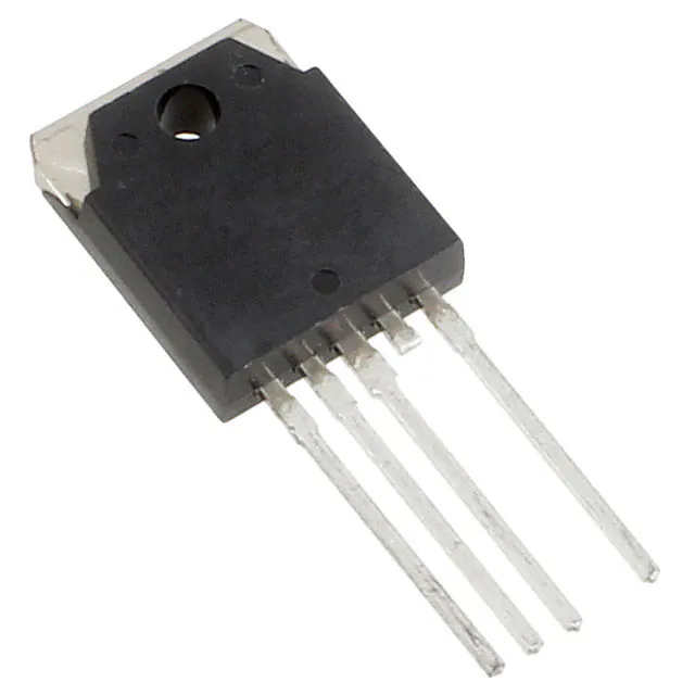
This device is provided in a 5-pin TO-3P plastic package with
pin 4 removed. Contact Sanken™ for application support and
additional information on device performance.
rN
Package: 5 pin TO-3P (MT-100)
Applications include:
STD01P
m
en
STD01N
de
d
fo
▪ General amplifier applications
▪ Professional audio amplifiers
▪ Car audio amplifiers
1 2 3 4
5
Not to scale
1 2 3 4
5
Equivalent Circuits
STD01N
3
4
STD01P
1
N
ot
R
ec
o
m
Emitter pins symmetrical
1
5
2
5
3
Datasheet 28104.011
�STD01N and
STD01P
Darlington Transistors for Audio Amplifiers
SELECTION GUIDE
Type
STD01N*
hFE Rating
Range O: 5000 to 12000
NPN
STD01P*
Packing
Range Y: 8000 to 20000
Bulk, 100 pieces
Range O: 5000 to 12000
PNP
Range Y: 8000 to 20000
ns
Part Number
es
ig
*Specify hFE range when ordering. If no hFE range is specified, order will be fulfilled with either or both range O and range Y,
depending upon availability.
Rating
Unit
VCBO
150
V
VCEO
150
V
VEBO
5
V
IC
10
A
IB
1
Collector-Base Voltage1
Collector-Emitter
Voltage1
Emitter-Base Voltage1
Collector Current1
Base
Current1
A
100
IF
10
Junction Temperature
TJ
150
°C
Storage Temperature
Tstg
–55 to150
°C
d
PNP type (STD01P), voltage and current values are negative.
2T = 25°C.
C
en
1For
W
mA
de
Collector Power
fo
PC
Diode Forward Current
Dissipation2
ew
Symbol
rN
Characteristic
D
ABSOLUTE MAXIMUM RATINGS at TA = 25°C
m
ELECTRICAL CHARACTERISTICS at TA = 25°C
Current1
Emitter Cutoff Current1
Collector-Emitter Voltage1
R
DC Current Transfer
Ratio2,3
Collector-Emitter Saturation
Voltage1
ot
Base-Emitter Saturation Voltage1
N
Base-Emitter Voltage
Diode Forward Voltage
Test Conditions
Min.
Typ.
Max.
Unit
ICBO
VCB = 150 V
–
–
100
μA
IEBO
VEB = 5 V
–
–
100
μA
VCEO
IC = 30 mA
150
–
–
V
hFE
VCE = 4 V, IC = 6 A
5000
–
20000
–
VCE(sat)
IC = 6 A, IB = 6 mA
–
–
–2.0
V
VBE(sat)
IC = 6 A, IB = 6 mA
–
–
–2.5
V
STD01N
VCE = 20 V, IC = 40 mA
–
1220
–
mV
STD01P
VCE = –20 V, IC = –40 mA
–
1230
–
mV
STD01N
IF = 2.5 mA
–
705
–
mV
STD01P
IF = 2.5 mA
–
1580
–
mV
ec
o
Collector-Cutoff
Symbol
m
Characteristic
VBE
VF
1For
PNP type (STD01P), voltage and current values are negative.
rating: 5000 to 12000(O brand on package), 8000 to 20000 (Y).
3When the transistor is used in pairs, the following conditions must be satisfied: Total V ≤ Total V
F
BE of the transistors (the above measurement
conditions shall be applied), and ∆V = 0 to 500 mV.
2h
FE
All performance characteristics given are typical values for circuit or
system baseline design only and are at the nominal operating voltage and
an ambient temperature of +25°C, unless otherwise stated.
Sanken Electric Co., Ltd.
3-6-3 Kitano, Niiza-shi, Saitama-ken
352-8666, Japan
Phone:+81-48-472-1111
http://www.sanken-ele.co.jp
2
�STD01N and
STD01P
Darlington Transistors for Audio Amplifiers
10 mA
10
2.
0m
A
STD01N Performance Characteristics at TA = 25°C
1.5
A
m
3
A
1.0 m
A
0.8 m
IC (A)
IC vs. VCE
VCE(sat) vs. IB
0.3 mA
4
2
8A
6A
IC= 4 A
ns
0.5 mA
6
VCE(sat) (V)
8
1
es
ig
IB= 0.2 mA
2
0
0
2
4
0
0.0001
6
VCE = 4 V Continuous
fo
°C
C
–30°
C
0.5
1.0
1.5
VBE (V)
2.0
2.5
m
Single pulse
No heatsink
Natural cooling
TA=25°
1000
1.0
IC (A)
m
100
1
10 0 m
0 s
DC ms
10.0
R
0.1
1.0
VF (V)
1.5
1
2.0
10
VCE (V)
N
100
80
ith
W
1.00
ite
in
k
in
ts
ea
H
PC vs. TA
0.10
PC (W)
60
f
In
RθJA (°C/W)
100
0.01
0.5
10.00
RθJA vs. t
10
100.0
Safe Operating
Area
ec
o
IF (mA)
ot
0
1
IC (A)
en
10
102
0.1
de
0
C
125°
25°C
C
–30°
104
103
d
25°
125
2
1
hFE
rN
IC (A)
hFE vs. IC
4
IF vs. VF
For Diode
1
105
6
0
0.1
ew
8
VCE = 4 V Continuous
0.01
IB (A)
106
10
IC vs. VBE
0.001
D
VCE (V)
40
20
0.01
3.5
1
10
t (ms)
100
1000
0
Without Heatsink
0
25
50
Sanken Electric Co., Ltd.
3-6-3 Kitano, Niiza-shi, Saitama-ken
352-8666, Japan
Phone:+81-48-472-1111
http://www.sanken-ele.co.jp
75
100
TA (°C)
125
150
3
�STD01N and
STD01P
Darlington Transistors for Audio Amplifiers
STD01P Performance Characteristics at TA = 25°C
A
A
0.8 mA
–IC (A)
8
IC vs. VCE
3
1.0 mA
m
0.5 mA
6
VCE(sat) vs. IB
0.3 mA
4
2
ns
1.5
–VCE(sat) (V)
2.
0m
10 mA
10
8A
6A
–IC = 4 A
–IB= 0.2 mA
0
0
2
4
0
0.0001
6
–VCE (V)
106
ew
10
8
0.5
1.0
1.5
–VBE (V)
2.5
m
Single pulse
No heatsink
Natural cooling
TA=25°
1000
1.0
IC (A)
m
100
1
10 0 m
0 s
DC ms
10.0
R
2.0
1
2.5
10
–VCE (V)
N
100
80
ith
W
1.00
fin
ite
si
at
He
PC vs. TA
40
nk
0.10
PC (W)
60
In
RθJA (°C/W)
100
0.1
1.0
1.5
VF (V)
10.00
RθJA vs. t
10
100.0
Safe Operating
Area
ec
o
IF (mA)
1
0.01
0.5
ot
0
C
–30°
–IC (A)
en
2.0
104
102
0.1
de
0
10
1
1
103
d
25°C
–30°
C
°C
125
fo
–VCE = 4 V Continuous
2
IF vs. VF
For Diode
hFE
hFE vs. IC
4
0
0.1
C
125°
25°C
rN
–IC (A)
–VCE = 4 V Continuous
0.01
–IB (A)
105
6
IC vs. VBE
0.001
D
2
es
ig
1
20
0.01
3.5
1
10
t (ms)
100
1000
0
Without Heatsink
0
25
50
75
100
TA (°C)
Sanken Electric Co., Ltd.
3-6-3 Kitano, Niiza-shi, Saitama-ken
352-8666, Japan
Phone:+81-48-472-1111
http://www.sanken-ele.co.jp
125
150
4
�STD01N and
STD01P
Darlington Transistors for Audio Amplifiers
PACKAGE OUTLINE DRAWING, TO-3P
STD01P
Terminal
Configuration
4.8 ±0.2
+0.2
1.34 –0.1
+0.2
+0.1
1.7 ±0.1
Terminal dimension
at case surface
+1
20.5 –0.5
fo
1.74 –0.1
3.2 –0.2
D
rN
3 MAX
XXXXXXXX
XXXXXXXX
(35.4)
14.9 ±0.2
Branding
+0.2
–0.1
es
ig
2
ew
Gate Burr
ns
2 ±0.2
15.6 ±0.3
19.9 ±0.3
STD01N
Terminal
Configuration
+0.2
en
de
d
1.05 –0.1
m
m
4×P2.54 ±0.1 = (10.16)
Terminal dimensions at case surface
3
4
5
4×P2.54 ±0.6 = 10.16 ±0.8
Terminal dimension at lead tips
15.8 ±0.2
ec
o
R
2
ot
1
1
2
3
4
5
N
Gate burr: 0.3 mm (max.), mold flash may appear at opposite side
Terminal core material: Cu
Terminal treatment: Ni plating and solder dip
Heat sink material: Cu
Heat sink treatment: Ni plating
Leadform: 2804
Weight (approximate): 6.0 g
Dimensions in millimeters
+0.2
0.65 –0.1
Branding codes (exact appearance at manufacturer discretion):
1st line, type: STD01X
Where: X is the transistor type (N or P)
2nd line, lot:
YMDD H
Where: Y is the last digit of the year of manufacture
M is the month (1 to 9, O, N, D)
DD is the 2-digit date
H is the hFE rating (O or Y; for values see
footnote, Electrical Characteristics table)
Leadframe plating Pb-free. Device composition
includes high-temperature solder (Pb >85%),
which is exempted from the RoHS directive.
Sanken Electric Co., Ltd.
3-6-3 Kitano, Niiza-shi, Saitama-ken
352-8666, Japan
Phone:+81-48-472-1111
http://www.sanken-ele.co.jp
5
�STD01N and
STD01P
Darlington Transistors for Audio Amplifiers
WARNING — These devices are designed to be operated at lethal voltages and energy levels. Circuit designs
that embody these components must conform with applicable safety requirements. Precautions must be
taken to prevent accidental contact with power-line potentials. Do not connect grounded test equipment.
ns
The use of an isolation transformer is recommended during circuit development and breadboarding.
de
d
fo
rN
ew
D
es
ig
Because reliability can be affected adversely by improper storage environments and handling methods, please
observe the following cautions.
Cautions for Storage
•
Ensure that storage conditions comply with the standard temperature (5°C to 35°C) and the standard relative
humidity (around 40 to 75%); avoid storage locations that experience extreme changes in temperature or
humidity.
•
Avoid locations where dust or harmful gases are present and avoid direct sunlight.
•
Reinspect for rust in leads and solderability of products that have been stored for a long time.
Cautions for Testing and Handling
When tests are carried out during inspection testing and other standard test periods, protect the products from
power surges from the testing device, shorts between adjacent products, and shorts to the heatsink.
Remarks About Using Silicone Grease with a Heatsink
• When silicone grease is used in mounting this product on a heatsink, it shall be applied evenly and thinly. If more
silicone grease than required is applied, it may produce stress.
• Volatile-type silicone greases may produce cracks after long periods of time, resulting in reduced heat radiation
effect. Silicone grease with low consistency (hard grease) may cause cracks in the mold resin when screwing the
product to a heatsink.
• Our recommended silicone greases for heat radiation purposes, which will not cause any adverse effect on the
product life, are indicated below:
Suppliers
en
Type
G746
Shin-Etsu Chemical Co., Ltd.
Dow Corning Toray Silicone Co., Ltd.
m
SC102
Toshiba Silicone Co., Ltd.
m
YG6260
ot
R
ec
o
Heatsink Mounting Method
• Torque When Tightening Mounting Screws. Thermal resistance increases when tightening torque is low, and radiation
effects are decreased. When the torque is too high, the screw can strip, the heatsink can be deformed, and distortion
can arise in the product frame. To avoid these problems, observe the recommended tightening torques for this product
package type, TO-3P (MT-100): 0.686 to 0.882 N•m (7 to 9 kgf•cm).
• Diameter of Heatsink Hole: < 4 mm. The deflection of the press mold when making the hole may cause the case material
to crack at the joint with the heatsink. Please pay special attention for this effect.
N
Soldering
•
When soldering the products, please be sure to minimize the working time, within the following limits:
260±5°C 10 s
350±5°C 3 s
• Soldering iron should be at a distance of at least 1.5 mm from the body of the products
Electrostatic Discharge
•
When handling the products, operator must be grounded. Grounded wrist straps worn should have at least 1 MΩ
of resistance to ground to prevent shock hazard.
•
Workbenches where the products are handled should be grounded and be provided with conductive table and
floor mats.
•
When using measuring equipment such as a curve tracer, the equipment should be grounded.
•
When soldering the products, the head of soldering irons or the solder bath must be grounded in other to prevent
leak voltages generated by them from being applied to the products.
•
The products should always be stored and transported in our shipping containers or conductive containers, or be
wrapped in aluminum foil.
Sanken Electric Co., Ltd.
3-6-3 Kitano, Niiza-shi, Saitama-ken
352-8666, Japan
Phone:+81-48-472-1111
http://www.sanken-ele.co.jp
6
�STD01N and
STD01P
de
d
fo
rN
ew
D
es
ig
ns
Darlington Transistors for Audio Amplifiers
en
The products described herein are manufactured in Japan by Sanken Electric Co., Ltd.
m
Sanken reserves the right to make, from time to time, such departures from the detail specifications as may be required to permit improvements in
the performance, reliability, or manufacturability of its products. Therefore, the user is cautioned to verify that the information in this publication is
current before placing any order.
ec
o
m
When using the products described herein, the applicability and suitability of such products for the intended purpose shall be reviewed at the users
responsibility.
Although Sanken undertakes to enhance the quality and reliability of its products, the occurrence of failure and defect of semiconductor products
at a certain rate is inevitable.
R
Users of Sanken products are requested to take, at their own risk, preventative measures including safety design of the equipment or systems
against any possible injury, death, fires or damages to society due to device failure or malfunction.
N
ot
Sanken products listed in this publication are designed and intended for use as components in general-purpose electronic equipment or apparatus
(home appliances, office equipment, telecommunication equipment, measuring equipment, etc.). Their use in any application requiring radiation
hardness assurance (e.g., aerospace equipment) is not supported.
When considering the use of Sanken products in applications where higher reliability is required (transportation equipment and its control systems
or equipment, fire- or burglar-alarm systems, various safety devices, etc.), contact a company sales representative to discuss and obtain written
confirmation of your specifications.
The use of Sanken products without the written consent of Sanken in applications where extremely high reliability is required (aerospace equipment, nuclear power-control stations, life-support systems, etc.) is strictly prohibited.
The information included herein is believed to be accurate and reliable. Application and operation examples described in this publication are
given for reference only and Sanken assumes no responsibility for any infringement of industrial property rights, intellectual property rights, or any
other rights of Sanken or any third party that may result from its use.
Copyright © 2007 Sanken Electric Co., Ltd.
Sanken Electric Co., Ltd.
3-6-3 Kitano, Niiza-shi, Saitama-ken
352-8666, Japan
Phone:+81-48-472-1111
http://www.sanken-ele.co.jp
7
�Darlington Transistors for Audio Amplifiers
STD01N and STD01P
August, 2007
Asia Pacific
China
es
ig
D
ew
Sanken Electric (Shanghai) Co., Ltd.
Room3202, Maxdo Centre, Xingyi Road 8, Changning district, Shanghai, China
Tel: 86-21-5208-1177
Fax: 86-21-5208-1757
ns
Sanken Electric Hong Kong Co., Ltd.
Suite 1026 Ocean Centre, Canton Road, Tsimshatsui, Kowloon, Hong Kong
Tel: 852-2735-5262
Fax: 852-2735-5494
rN
India
d
fo
Saket Devices Pvt. Ltd.
Office No.13, First Floor, Bandal - Dhankude Plaza, Near PMT Depot, Paud Road, Kothrud, Pune - 411 038, India
Tel: 91-20-5621-2340
91-20-2528-5449
Fax: 91-20-2528-5459
de
Japan
m
en
Sanken Electric Co., Ltd. Overseas Sales Headquaters
Metropolitan Plaza Bldg. 1-11-1 Nishi-Ikebukuro, Toshima-ku, Tokyo 171-0021, Japan
Tel: 81-3-3986-6164
Fax: 81-3-3986-8637
m
Korea
Singapore
R
ec
o
Sanken Electric Korea Co., Ltd.
Mirae Asset Life Bldg. 6F, 168 Kongduk-dong, Mapo-ku, Seoul, 121-705, Korea
Tel: 82-2-714-3700
Fax: 82-2-3272-2145
N
ot
Sanken Electric Singapore Pte. Ltd.
150 Beach Road, #14-03 The Gateway West, Singapore 189720
Tel: 65-6291-4755
Fax: 65-6297-1744
Taiwan
Taiwan Sanken Electric Co., Ltd.
Room 1801, 18th Floor, 88 Jung Shiau East Road, Sec. 2, Taipei 100, Taiwan R.O.C.
Tel: 886-2-2356-8161
Fax: 886-2-2356-8261
Sanken Electric Co., Ltd.
T02-012EA-070820
�Darlington Transistors for Audio Amplifiers
STD01N and STD01P
August, 2007
Europe
United Kingdom
ns
Sanken Power Systems (UK) Limited
Pencoed Technology Park Pencoed, Bridgend CF35 5HY. UK
Tel: 44-1656-869-100
Fax: 44-1656-869-162
es
ig
North America
ew
fo
N
ot
R
ec
o
m
m
en
de
d
Allegro MicroSystems, Inc. (Southern California)
14 Hughes Street, Suite B105, Irvine, CA 92618
Tel: 1-949-460-2003
Fax: 1-949-460-7837
rN
Allegro MicroSystems, Inc.
115 Northeast Cutoff, Worcester, Massachusetts 01606, U.S.A.
Tel: 1-508-853-5000
Fax: 1-508-853-3353
D
United States
Sanken Electric Co., Ltd.
T02-012EA-070820
�


 工商网监
湘ICP备2023018690号
工商网监
湘ICP备2023018690号
