Ordering number : ENN7632
LC75700T
CMOS IC
Key Scan IC
http://onsemi.com
Overview
The LC75700T is a key scanning LSI that accepts input from up to 30 keys and can control up to four general
purpose output ports. Therefore it can reduce the number of lines to the front panel in application systems.
Features
Key input function for up to 30 keys.
General-purpose output ports for up to four pins.
A key scan is performed only when a key is pressed, and thus power dissipation is reduced.
Serial data I/O supports CCB format communication with the system controller.
Switching between the key scan output port and general purpose output port functions can be controlled by the
control data.
The RES pin is provided. This pin disables key scanning, and forces the general-purpose output ports to the low
level.
RC oscillator circuit
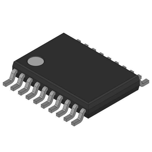
TSSOP20(225mil)
ORDERING INFORMATION
Device
LC75700T-MPB-E
Package
TSSOP20(225mil)
(Pb-Free)
LC75700T-TLM-E
TSSOP20(225mil)
(Pb-Free)
2000 / Tape &Reel
LC75700TS-MPB-E
TSSOP20(225mil)
(Pb-Free)
70 / Fan-Fold
LC75700TS-TLM-E
TSSOP20(225mil)
(Pb-Free)
2000 / Tape &Reel
Shipping (Qty / Packing)
70 / Fan-Fold
CCB is ON Semiconductor® ’s original format. All addresses are managed
by ON Semiconductor® for this format.
CCB is a registered trademark of Semiconductor Components Industries, LLC.
Semiconductor Components Industries, LLC, 2013
October, 2013
13004TN(OT) No.7632-1/16
�LC75700T
Specifications
Absolute Maximum Ratings at Ta = 25°C, VSS = 0 V
Parameter
Maximum supply voltage
Input voltage
Output voltage
Output current
Allowable power dissipation
Symbol
VDD max
Conditions
Ratings
Unit
VDD
–0.3 to +7.0
VIN1
CE, CL, DI, RES
–0.3 to +7.0
VIN2
OSC, KI1 to KI5
–0.3 to VDD + 0.3
VOUT1
DO
VOUT2
OSC, KS1 to KS6, P1 to P4
IOUT1
KS1 to KS6
1
IOUT2
P1 to P4
5
Pd max
–0.3 to +7.0
–0.3 to VDD + 0.3
Ta = 85°C
150
V
V
V
mA
mW
Operating temperature
Topr
–40 to +85
°C
Storage temperature
Tstg
–50 to +150
°C
Allowable Operating Ranges at Ta = –40 to +85°C, VSS = 0 V
Parameter
Supply voltage
Input high level voltage
Input low level voltage
Symbol
Ratings
Conditions
min
typ
max
VDD
VDD
VIH1
CE, CL, DI, RES
0.8 VDD
5.5
VIH2
KI1 to KI5
0.6 VDD
VDD
VIL
2.7
CE, CL, DI, RES, KI1 to KI5
Recommended external resistance
Rosc
Recommended external capacitance
Cosc
OSC
Guaranteed oscillator range
fosc
OSC
5.0
0
OSC
5.5
0.2 VDD
39
38
V
V
V
kΩ
1000
19
Unit
pF
76
kHz
Low level clock pulse width
tøL
CL
See figure 1.
160
ns
High level clock pulse width
tøH
CL
See figure 1.
160
ns
ns
Data setup time
tds
DI, CL
See figure 1.
160
Data hold time
tdh
DI, CL
See figure 1.
160
ns
CE wait time
tcp
CE, CL
See figure 1.
160
ns
CE setup time
tcs
CE, CL
See figure 1.
160
ns
CE hold time
tch
CE, CL
See figure 1.
160
ns
DO output delay time
tdc
DO RPU = 4.7 kΩ, CL = 10 pF*1 See figure 1.
1.5
µs
DO rise time
tdr
DO RPU = 4.7 kΩ, CL = 10 pF*1 See figure 1.
1.5
µs
Note: *1. Since DO is an open-drain output, these times depend on the values of the pull-up resistor RPU and the load capacitance CL.
No. 7632-2/16
�LC75700T
Electrical Characteristics in the Allowable Operating Ranges
Parameter
Symbol
Pin Name
Hysteresis
VH
CE, CL, DI, RES, KI1 to KI5
Input high level current
IIH
CE, CL, DI, RES
VI = 5.5 V
Input low level current
IIL
CE, CL, DI, RES
VI = 0 V
Input floating voltage
VIF
KI1 to KI5
Pull-down resistance
Output off leakage current
Output high level voltage
RPD
IOFFH
VOH1
VOH2
VOL1
Current drain
typ
Unit
max
V
5
–5
KI1 to KI5
DO
VDD = 5.0 V
50
100
250
VDD = 3.0 V
100
200
500
VO = 5.5 V
KS1 to KS6
P1 to P4
KS1 to KS6
6
VDD = 3.6 V to 5.5 V
IO = –500 µA
VDD – 1.0
VDD – 0.5
VDD – 0.2
VDD = 2.7 V to 3.6 V
IO = –250 µA
VDD – 0.8
VDD – 0.4
VDD – 0.1
IO = –1 mA
VDD – 0.9
VDD = 3.6 V to 5.5 V
IO = 25 µA
0.2
0.5
1.5
VDD = 2.7 V to 3.6 V
IO = 12.5 µA
0.1
0.4
1.2
P1 to P4
IO = 1 mA
VOL3
DO
IO = 1 mA
fosc
OSC
Rosc = 39 kΩ
Cosc = 1000 pF
IDD1
VDD
Key scan standby state
VDD
VDD = 5.5 V
Output open
fosc = 38 kHz
µA
µA
0.05 VDD
VOL2
IDD2
min
0.1 VDD
Output low level voltage
Oscillator frequency
Ratings
Conditions
V
kΩ
µA
V
V
0.9
30.4
0.1
0.5
38
45.6
kHz
5
200
400
µA
20
KS6/P2
P1
VSS
VDD
OSC
RES
DO
CE
CL
DI
Pin Assignment
11
LC75700T
P3/KS5
KS3
P4/KS4
KS2
KS1
KI5
KI4
KI3
10
KI2
KI1
1
Top view
No. 7632-3/16
�LC75700T
1. When CL is stopped at the low level
VIH1
CE
tøH
CL
VIL
tøL
VIH1
50%
VIL
tcp
DI
tch
tcs
VIH1
VIL
tds
tdh
DO
D0
D1
tdr
tdc
2. When CL is stopped at the high level
VIH1
CE
tøL
CL
tøH
VIH1
50%
VIL
tcp
DI
tcs
tch
VIH1
VIL
tds
DO
VIL
tdh
D0
D1
tdc
tdr
Figure 1
No. 7632-4/16
�LC75700T
P1
KS6/P2
KS5/P3
KS3
KS4/P4
KS2
KS1
KI5
KI4
KI3
KI2
KI1
Block Diagram
VDD
KEY SCAN
VSS
KEY BUFFER
GENERAL PORT
CLOCK
GENERATOR
OSC
CONTROL REGISTER
CCB
INTERFACE
RES
DO
CE
CL
DI
SHIFT REGISTER
No. 7632-5/16
�LC75700T
Pin Functions
Pin
Pin No.
Active
I/O
Handling when unused
KI1 to KI5
1 to 5
Key scan inputs. These pins have built-in pull-down resistors.
H
I
GND
KS1 to KS3
6 to 8
Key scan outputs. Although normal key scan timing lines require diodes to be
inserted in the timing lines to prevent shorts, since these outputs are unbalanced
CMOS transistor outputs, these outputs will not be damaged by shorting when
these outputs are used to from a key matrix.
—
0
Open
KS4/P4 to KS6/P2
9 to 11
—
0
Open
P1
12
—
0
Open
—
I/O
VDD
L
I
GND
H
I
▲
I
—
I
OSC
14
Function
Key scan outputs and general-purpose output ports shared-function pins.
These pins can be set the key scan output ports or the general-purpose output
ports by the control data “KP1 and KP2”.
The P1 is general-purpose output ports.
Oscillator connection. An oscillator circuit is formed by connecting an external
resistor and capacitor at this pin.
DO
17
Reset input. that re-initializes the LSI internal states. This pin must be used.
• When RES is low (VSS)
— Key scanning disabled: KS1 to KS3 = low (VSS).
— Key scan outputs and general output ports shared-function pins:
KS4/P4 to KS6/P2 = low (VSS).
— General-purpose output port: P1 = low (VSS).
— All the key data is reset to low.
• When RES is high (VDD)
— The states of the pins as key scan output pins or general-purpose output
ports, must be set with the control data.
— And key scanning is a enabled.
Note that serial data must be transferred when RES is high.
Serial data interface. Connections to the controller. Note that DO, being
an open-drain output, requires a pull-up resistor.
CE: Chip enable
CL: Synchronization clock
DI: Transfer data
DO: Output data
—
O
Open
VDD
15
Power supply. A voltage of between 2.7 V and 5.5 V must be supplied.
—
—
—
VSS
13
Ground. Must be connected to the system ground.
—
—
—
RES
16
CE
18
CL
19
DI
20
GND
No. 7632-6/16
�LC75700T
Serial Data Input
1. When CL is stopped at the low level
CE
CL
DI
0
1
B0
B1
1
1
0
B2 B3 A0 A1
CCB address
0
0
0
A2
A3
KC1 KC2 KC3 KC4 KC5 KC6
0
0
PC1 PC2 PC3 PC4
0
0
KP1 KP2
0
0
KP1 KP2
Control data
DO
2. When CL is stopped at the high level
CE
CL
DI
0
1
B0
B1
1
1
0
B2 B3 A0 A1
CCB address
0
0
0
A2
A3
KC1 KC2 KC3 KC4 KC5 KC6
0
0
PC1 PC2 PC3 PC4
Control data
DO
• CCB address: 62H
• KC1 to KC6: Key scan output state setting data
• PC1 to PC4: General-purpose output port state setting data
• KP1, KP2: Selection data between the key scan output ports and the general-purpose output ports.
No. 7632-7/16
�LC75700T
Control Data Functions
1.KP1, KP2: Selection data between the key scan output ports and the general-purpose output ports.
These control data bits switch the functions of the KS4/P4 to KS6/P2 output pins between the key scan output port and
the general-purpose output port.
KP1
KP2
0
1
Output pins
Maximum number
of key inputs
Number of general-purpose
output ports (+ P1)
KS4/P4
KS5/P3
KS6/P2
0
KS4
KS5
KS6
30
0 (+1)
0
KS4
KS5
P2
25
1 (+1)
0
1
KS4
P3
P2
20
2 (+1)
1
1
P4
P3
P2
15
3 (+1)
Note: KSn (n = 4 to 6): Key scan output ports
Pn (n = 4 to 2): General-purpose output ports
2.KC1 to KC6: Key scan output state setting data
These control data bits set the states of the key scan output pins KS1 to KS6.
Output pins
KS1
KS2
KS3
KS4
KS5
KS6
Key scan output state setting data
KC1
KC2
KC3
KC4
KC5
KC6
For example, if the KS4/P4 to KS6/P2 output pins are set to function as key scan output ports, when KC1 to KC3 are
set to 1 and KC4 to KC6 are set to 0, in the key scan standby state, the KS1 to KS3 output pins will output the high
level (VDD) and the KS4 to KS6 pins will output the low level (VSS). Note that key scan output signals are not output
from output pins that are set to the low level.
3.PC1 to PC4: General-purpose output port state setting data
These control data bits set the states of the general-purpose output ports P1 to P4.
Output pins
P1
P2
P3
P4
General-purpose output port state setting data
PC1
PC2
PC3
PC4
For example, if the KS4/P4 to KS6/P2 output pins are set to function as general-purpose output ports, when PC1 and
PC2 are set to 1, and PC3 and PC4 are set to 0, the P1 and P2 output pins will output the high level (VDD), and P3 and
P4 will output the low level (VSS).
No. 7632-8/16
�LC75700T
Serial Data Output
1. When CL is stopped at the low level
CE
CL
DI
1
1
B0
B1
0
0
0
1
B2 B3 A0 A1
CCB address
1
0
A2
A3
DO
X KD1 KD2 KD3
KD26 KD27 KD28 KD29 KD30
X
Output data
X : don’t care
2. When CL is stopped at the high level
CE
CL
DI
1
1
0
B0
B1
B2
0
0
1
B3 A0 A1
CCB address
1
0
A2
A3
DO
X KD1 KD2 KD3 KD4
KD26 KD27 KD28 KD29 KD30
X
X
Output data
X : don’t care
• CCB address: 63H
• KD1 to KD30: Key data
Note: If a key data read operation is executed when DO is high, the read key data (KD1 to KD30) will be invalid.
Output Data
1.KD1 to KD30: Key data
When a key matrix of up to 30 keys is formed from the KS1 to KS6 key scan output pins and the KI1 to KI5 key scan
input pins and one of those key is pressed, the key output data corresponding to that key will be set to 1. The table
shows the relationship between those pins and the key data bits.
KS1
KI1
KI2
KI3
KI4
KI5
KD1
KD2
KD3
KD4
KD5
KS2
KD6
KD7
KD8
KD9
KD10
KS3
KD11
KD12
KD13
KD14
KD15
KS4
KD16
KD17
KD18
KD19
KD20
KS5
KD21
KD22
KD23
KD24
KD25
KS6
KD26
KD27
KD28
KD29
KD30
When the KS4/P4 to KS6/P2 output pins are set to function as the general-purpose output ports with the control data
“KP1 and KP2”, and a key matrix of up to 15 keys is formed from the KS1 to KS3 output pins and the KI1 to KI5 input
pins, the KD16 to KD30 key data bits will be set to 0.
No. 7632-9/16
�LC75700T
Key Scan Operation Functions
1.Key scan timing
The key scan period is 288T (s). To reliably determine the on/off state of the keys, this LSI scans the keys twice and
determines that a key has been pressed when the key data agrees. It outputs a key data read request (a low level on DO)
615T (s) after starting a key scan. If the key data does not agree and a key was pressed at that point, it scans the keys
again. Thus this LSI cannot detect a key press shorter than 615T (s).
KS1
*2
KS2
*2
KS3
*2
1
1
2
*2
2
3
*2
3
*2
T=
KS4
*2
KS5
*2
KS6
*2
4
4
5
*2
5
*2
6
Key on
1
fosc
6
*2
576T[s]
*2. Not that the high/low states of these pins are determined by the control data, and that key scan output signals are not output
from pins that are set to low .
2.Key scan operation
•The pins KS1 to KS6 are set to the high or low state by the control data.
•If a key on one of the lines corresponding to a KS1 to KS6 pin which is set high is pressed, the oscillator on the OSC
pin is started and a key scan is performed. Keys are scanned until all keys are released. Multiple key presses are
recognized by determining whether multiple key data bits are set.
•If a key is pressed for longer than 615T (s) (where T = 1/fosc) this LSI outputs a key data read request (a low level on
DO) to the controller. The controller acknowledges this request and reads the key data. However, if CE is high during a
serial data transfer, Do will be set high.
•After the controller reads the key data, the key data read request is cleared (DO is set high) and this LSI performs
another key scan. Also note that DO being an open-drain output, requires a pull-up resistor (between 1 kΩ and 10 kΩ) .
Key input 1
Key input 2
Key scan
615T[s]
615T[s]
615T[s]
CE
Serial data transfer
Serial data transfer Key address (63H) Serial data transfer
Key address
Key address
DI
DO
Key data read
Key data read request
Key data read
Key data read request
Key data read
Key data read request
T=
1
fosc
No. 7632-10/16
�LC75700T
Example: When control data “KP1 and KP2 = 0, KC1 to KC5 = 0, KC6 = 1” are executed.
(i.e.key scanning with only KS6 high.)
[L] KS1
[L] KS2
When any one of these keys is pressed, the
oscillator on the OSC pin is started and the
keys are scanned.
[L] KS3
[L] KS4
[L] KS5
[H] KS6
*3
KI1
KI2
KI3
KI4
KI5
*3. These diodes are required to reliabled recognize multiple key presses of keys on the KS6 line when state with
only KS6 high, as in the above example. That is, these diodes prevent incorrect operations due to sneak currents
in the KS6 key scan output signal keys on the KS1 to KS5 lines are pressed at the same time.
Key input
(KS6 line)
Key scan
615T[s]
615T[s]
CE
Serial data transfer
Serial data transfer
Key address (63H)
Serial data transfer
Key address
T=
1
fosc
DI
DO
Key data read
Key data read request
Key data read
Key data read request
Multiple Key Presses
Although this LSI is capable of key scanning without inserting diodes for dual key presses, triple key presses on the
KI1 to KI5 input pin lines, or multiple key presses on the KS1 to KS6 output pin lines, multiple presses other than these
cases may result in keys that were not pressed recognized as having been pressed. Therefore, a diode must be inserted
in series with each key.Applications that do not recognize multiple key presses of three or more keys should check the
key data for three or more 1 bits and ignore such data.
No. 7632-11/16
�LC75700T
System Reset
When the power is first applied, the state of function is undefined, so it must be initialized by RES = “L”
1.Reset methods
This LSI stopprts the reset methods described below.
When a system reset is applied, key scanning is disabeled, the key data is reset, and the general-purpose output ports
are set to and held at the low level (VSS).
Set RES = “H” after the RES = “L” period. And key scanning become possible by the control data are transferred.
VDDmin
VDD
t1
VIH1
RES
VIL
CE
t2
VIL
Control data transfer
KS1 to KS3
Output pins KS4/P4 to KS6/P2
P1
"L"
Undefined
Defined
Notes: t1 ≥ 10 µs
t2 ≥ 10 µs
P1
KS1
KS2
KS3
KS4/P4
KS5/P3
KS6/P2
KI1
KI2
KI3
KI4
KI5
2.Internal block states during the reset period.
• CLOCK GENERATOR
Reset is applied and the basic clock is stopped. (The oscillator on the OSC pin is stopped.)
• KEY SCAN, KEY BUFFER
Reset is applied, the circuit is set to the initial state, and at the same time the key scan operation is disabled.
And all the key data is set to Low. Then, when the control data are transferred, the key scanning operation is enabled.
• GENERAL PORT
Reset is applied and the outputs of P1 to P4 are all set to the low level.
• CCB INTERFACE, SHIFT REGISTER, CONTROL REGISTER
When a reset is applied, The CONTROL REGISTER is forcibly initialized internally. Then, when control data are
transferred, the LSI operates according to the control data.
VDD
KEY SCAN
VSS
KEY BUFFER
GENERAL PORT
CLOCK
GENERATOR
OSC
CONTROL REGISTER
SHIFT REGISTER
RES
DO
CE
CL
DI
CCB
INTERFACE
Blocks to which the reset applies.
No. 7632-12/16
�LC75700T
3. Output pin states during a reset
Output pins
State during a reset
KS1 to KS3
L
KS4/P4 to KS6/P2
L
P1
L
DO
H *4
*4. Since this output pin is an open-drain output, a pull-up resistor of between 1 and 10 kΩ is required. This pin remains high during the reset period even if a
key data read operation is performed.
Sample Application Circuit
+5 V
VDD
OSC
P1
VSS
*7
RES *5
CE
CL
DI
DO
From the controller
To the controller
To the controller
power supply
(P1)
(P2)
(P3)
(P4)
(General-purpose output ports)
Used with the backlight
controller or other circuit.
KS6/P2
KS5/P3
KS4/P4
KS3
KS2
KS1
KI5
KI4
KI3
KI2
KI1
Key matrix
(up to 30 keys)
*6
Note: *5. When the power is first applied, it must be initialized by RES = "L".
*6. The DO pin,being an open-drain output, requires a pull-up resistor. Select a resistance (between 1 and 10 kΩ) appropriate
for the capacitance of the external wiring so that signal waveforms are not degraded.
*7. Each of The KS4/P4 to KS6/P2 pins must be set to either the key scan output port or the general-purpose output port.
No. 7632-13/16
�LC75700T
Notes on the controller key data read techniques
1. Timer based key data acquisition
(1) Flowchart
CE = "L"
NO
DO = "L"
YES
Key data read
processing
(2) Timing chart
Key on
Key on
Key input
Key scan
t3
t4
t3
t3
CE
t6
Key
address
DI
t5
Key data read
t6
t6
t5
t5
DO
Key data read request
t7
Controller
determination
(Key on)
t7
Controller
determination
(Key on)
t7
Controller
determination
(Key off)
t7
Controller
determination
(Key on)
t3: Key scan execution time when the key data agreed for two key scans (615T (s))
t4: Key scan execution time when the key data did not agree for two key scans and
the key scan was executed again. (1230T(s))
t5: Key address (63H) transfer time
t6: Key data read time
Controller
determination
(Key off)
T=
1
fosc
(3) Explanation
In this technique, the controller uses a timer to determine key on/off states and read the key data. The controller must
check the DO state when CE is low every t7 period without fail. If DO is low, the controller recognizes that a key has
been pressed and executed the key data read operation.
The period t7 in this technique must satisfy the following condition.
t7 > t4 + t5 + t6
If a keydata read operation is executed when DO is high, the read key data (KD1 to KD30) will be invalid.
No. 7632-14/16
�LC75700T
2. Interrupt based key data acquisition
(1) Flowchart
CE = "L"
No
DO = "L"
YES
Key data read
processing
Wait time of
at least t8
CE = "L"
NO
DO = "H"
YES
Key OFF
(2) Timing chart
Key on
Key on
Key input
Key scan
t3
t3
t4
t3
CE
t6
Key
address
DI
t5
t6
Key data read
t6
t5
t6
t5
t5
DO
Key data read request
t8
Controller
determination
(Key on)
t8
Controller
determination
(Key off)
Controller
determination
(Key on)
t8
Controller
determination
(Key on)
t8
Controller
determination
(Key on)
Controller
determination
(Key off)
t3: Key scan execution time when the key data agreed for two key scans (615T (s))
t4: Key scan execution time when the key data did not agree for two key scans and
the key scan was executed again. (1230T(s))
1
t5: Key address (63H) transfer time
T=
fosc
t6: Key data read time
No. 7632-15/16
�LC75700T
(3) Explanation
In this technique, the controller uses interrupts to determine key on/off states and read the key data. The controller
must check the DO state when CE is low. If DO is low, the controller recognizes that a key has been pressed and
executes the key data read operation. After that the next key on/off determination is performed after the time t8 has
elapsed by checking the DO state when CE is low and reading the key data.
The period t8 in this technique must satisfy the following condition.
t8 > t4
If a key data read operation is executed when DO is high, the read key data (KD1 to KD30) will be invalid.
Package Dimensions
unit : mm
TSSOP20 4.4x6.5 / TSSOP20 (225 mil)
CASE 948AX
ISSUE A
SOLDERING FOOTPRINT*
5.80
1.0
(Unit: mm)
0.32
GENERIC
MARKING DIAGRAM*
XXXXXXXXXX
YMDDD
0.65
NOTE: The measurements are not to guarantee but for reference only.
*For additional information on our Pb−Free strategy and soldering
details, please download the ON Semiconductor Soldering and
Mounting Techniques Reference Manual, SOLDERRM/D.
XXXXX = Specific Device Code
Y = Year
M = Month
DDD = Additional Traceability Data
*This information is generic. Please refer to
device data sheet for actual part marking.
ON Semiconductor and the ON logo are registered trademarks of Semiconductor Components Industries, LLC (SCILLC). SCILLC owns the rights to a number
of patents, trademarks, copyrights, trade secrets, and other intellectual property. A listing of SCILLC’s product/patent coverage may be accessed at
www.onsemi.com/site/pdf/Patent-Marking.pdf. SCILLC reserves the right to make changes without further notice to any products herein. SCILLC makes no
warranty, representation or guarantee regarding the suitability of its products for any particular purpose, nor does SCILLC assume any liability arising out of the
application or use of any product or circuit, and specifically disclaims any and all liability, including without limitation special, consequential or incidental
damages. “Typical” parameters which may be provided in SCILLC data sheets and/or specifications can and do vary in different applications and actual
performance may vary over time. All operating parameters, including “Typicals” must be validated for each customer application by customer’s technical
experts. SCILLC does not convey any license under its patent rights nor the rights of others. SCILLC products are not designed, intended, or authorized for use
as components in systems intended for surgical implant into the body, or other applications intended to support or sustain life, or for any other application in
which the failure of the SCILLC product could create a situation where personal injury or death may occur. Should Buyer purchase or use SCILLC products for
any such unintended or unauthorized application, Buyer shall indemnify and hold SCILLC and its officers, employees, subsidiaries, affiliates, and distributors
harmless against all claims, costs, damages, and expenses, and reasonable attorney fees arising out of, directly or indirectly, any claim of personal injury or
death associated with such unintended or unauthorized use, even if such claim alleges that SCILLC was negligent regarding the design or manufacture of the
part. SCILLC is an Equal Opportunity/Affirmative Action Employer. This literature is subject to all applicable copyright laws and is not for resale in any manner.
PS No.7632-16/16
�


 工商网监
湘ICP备2023018690号
工商网监
湘ICP备2023018690号
