Ordering number : EN3096A
2SA1709/2SC4489
Bipolar Transistor
http://onsemi.com
(-)100V, (-)2A, Low VCE(sat), (PNP)NPN Single NMP
Features
•
•
Adoption of FBET, MBIT processes
Fast switching speed
•
High breakdown voltage, large current capacity
( )2SA1709
Specifications
Absolute Maximum Ratings at Ta=25°C
Parameter
Symbol
Collector-to-Base Voltage
Conditions
Ratings
Unit
VCBO
VCEO
(--)120
(--)100
V
VEBO
IC
(--)6
V
(--)2
A
(--)3
A
Collector Dissipation
ICP
PC
1
W
Junction Temperature
Tj
Storage Temperature
Tstg
Collector-to-Emitter Voltage
Emitter-to-Base Voltage
Collector Current
Collector Current (Pulse)
V
150
°C
--55 to +150
°C
Stresses exceeding Maximum Ratings may damage the device. Maximum Ratings are stress ratings only. Functional operation above the Recommended Operating
Conditions is not implied. Extended exposure to stresses above the Recommended Operating Conditions may affect device reliability.
Package Dimensions
Product & Package Information
unit : mm (typ)
7540-001
• Package : NMP(Taping)
• JEITA, JEDEC : SC-71
• Minimum Packing Quantity : 2,500 pcs./box
2.5
6.9
1.05
2SA1709S-AN
2SA1709T-AN
2SC4489S-AN
2SC4489T-AN
1.0
4.5
1.0
1.45
Marking(NMP(Taping))
A1709
RANK
C4489
LOT No.
RANK
LOT No.
0.6
1.0
0.5
15.0
0.9
1
2.54
2
3
0.45
2.54
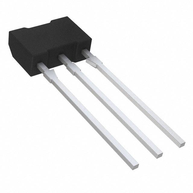
1 : Emitter
2 : Collector
3 : Base
NMP(Taping)
Electrical Connection
2
3
2
3
1
2SA1709
Semiconductor Components Industries, LLC, 2013
September, 2013
1
2SC4489
82912 TKIM TC-00002803/40804TN(PC)/5169MO, TS No.3096-1/7
�2SA1709 / 2SC4489
Electrical Characteristics at Ta=25°C
Parameter
Symbol
Collector Cutoff Current
ICBO
IEBO
VCB=(--)100V, IE=0A
VEB=(--)4V, IC=0A
VCE=(--)5V, IC=(--)100mA
Gain-Bandwidth Product
hFE
fT
Output Capacitance
Cob
Collector-to-Emitter Saturation Voltage
VCE(sat)
VBE(sat)
VCB=(--)10V, f=1MHz
IC=(--)1A, IB=(--)100mA
Emitter Cutoff Current
DC Current Gain
Base-to-Emitter Saturation Voltage
Collector-to-Base Breakdown Voltage
Emitter-to-Base Breakdown Voltage
Turn-On Time
Storage Time
Fall Time
min
typ
Unit
max
140*
(--)100
nA
(--)100
nA
400*
VCE=(--)10V, IC=(--)100mA
V(BR)CBO
V(BR)CEO
Collector-to-Emitter Breakdown Voltage
Ratings
Conditions
120
MHz
(25)16
pF
(--0.22)0.13
(--0.6)0.4
V
(--)0.85
(--)1.2
V
IC=(--)1A, IB=(--)100mA
IC=(--)10μA, IE=0A
(--)120
V
IC=(--)1mA, RBE=∞
(--)100
V
V(BR)EBO
ton
IE=(--)10μA, IC=0A
(--)6
tstg
tf
See specified Test Circuit.
V
80
ns
(750)1000
ns
(40)50
ns
* : The 2SA1709/2SC4489 are classified by 100mA hFE as follows :
Rank
S
T
hFE
140 to 280
200 to 400
Switching Time Test Circuit
2SA1709
2SC4489
IB1
IB2
PW=20μs
D.C.≤1%
VR
RB
100μF
PW=20μs
D.C.≤1%
RL
+
+
50Ω
IB2
OUTPUT
INPUT
IB1
RB
VR
+
+
50Ω
470μF
VBE=5V
OUTPUT
INPUT
100μF
470μF
VBE= --5V
VCC= --50V
IC=10IB1= --10IB2= --0.7A
RL
VCC=50V
IC=10IB1= --10IB2=0.7A
Ordering Information
Package
Shipping
2SA1709S-AN
Device
NMP(Taping)
2,500pcs./bag
2SA1709T-AN
NMP(Taping)
2,500pcs./bag
2SC4489S-AN
NMP(Taping)
2,500pcs./bag
2SC4489T-AN
NMP(Taping)
2,500pcs./bag
IC -- VCE
2SA1709
A
A
--1.6
0
--3
0m
--4
IC -- VCE
2SC4489
A
50m
A
--20m
0m
--5
--10mA
--1.2
Pb Free
2.0
mA
Collector Current, IC -- A
Collector Current, IC -- A
--2.0
memo
--0.8
--5mA
--0.4
--3mA
--2mA
1.6
20mA
1.2
10mA
5mA
0.8
3mA
2mA
0.4
--1mA
0
0
1mA
IB=0A
--1
--2
--3
--4
Collector-to-Emitter Voltage, VCE -- V
40mA
30mA
--5
ITR04340
0
IB=0A
0
1
2
3
4
Collector-to-Emitter Voltage, VCE -- V
5
ITR04341
No.3096-2/7
�2SA1709 / 2SC4489
IC -- VCE
A
--5mA
--4mA
--0.8
Collector Current, IC -- A
Collector Current, IC -- A
--6m
--3mA
--0.6
IC -- VCE
1.0
2SA1709
.5mA
5.0
mA
--1.0
--2mA
--0.4
--1mA
--0.2
4
2SC4489
4.0mA
3.5mA
0.8
3.0mA
0.6
2.5mA
2.0mA
0.4
1.5mA
1.0mA
0.2
0.5mA
0
0
IB=0A
--10
--20
--30
--40
0
--50
IB=0A
0
10
Collector-to-Emitter Voltage, VCE -- V ITR04342
IC -- VBE
Collector Current, IC -- A
75°C
25°C
--25°C
Ta=
Collector Current, IC -- A
--1.2
--0.4
--0.2
--0.4
--0.6
--0.8
--1.0
Base-to-Emitter Voltage, VBE -- V
0.8
0
--1.2
0.4
0.6
0.8
1.0
Base-to-Emitter Voltage, VBE -- V
2SC4489
VCE=5V
7
5
1.2
ITR04345
hFE -- IC
1000
2SA1709
VCE= --5V
7
0.2
ITR04344
hFE -- IC
1000
5
DC Current Gain, hFE
DC Current Gain, hFE
1.2
0
0
Ta=75°C
25°C
--25°C
3
2
100
7
3
2
Ta=75°C
25°C
--25°C
100
7
5
5
3
7 --0.01
2
3
5
7 --0.1
2
3
5
7 --1.0
Collector Current, IC -- A
2
100
7
5
3
2
3
5
7 --0.1
2
3
5
3
5
Collector Current, IC -- A
7 --1.0
2
3
ITR04348
7 0.1
2
3
5
7 1.0
Collector Current, IC -- A
Gain-Bandwidth Product, f T -- MHz
2SA1709
VCE= --10V
2
2
2
3
ITR04347
f T -- IC
3
2
7 --0.01
3
7 0.01
3
ITR04346
f T -- IC
3
Gain-Bandwidth Product, f T -- MHz
1.6
0.4
0
10
50
2SC4489
VCE=5V
2.0
--1.6
--0.8
40
IC -- VBE
2.4
2SA1709
VCE= --5V
--2.0
30
Ta=7
5°C
25°C
--25°C
--2.4
20
Collector-to-Emitter Voltage, VCE -- V ITR04343
2SC4489
VCE=10V
2
100
7
5
3
2
10
7 0.01
2
3
5
7 0.1
2
3
5
Collector Current, IC -- A
7 1.0
2
3
ITR04349
No.3096-3/7
�2SA1709 / 2SC4489
Cob -- VCB
100
Output Capacitance, Cob -- pF
5
3
2
10
7
5
3
7 --1.0
2
3
5
7 --10
2
3
5
VCE(sat) -- IC
Collector-to-Emitter
Saturation Voltage, VCE(sat) -- mV
5
3
2
--100
7
C
25°
5
C
Ta=75°
3
2
--10
--25°C
7 --0.01
2
3
5
7 --0.1
2
3
5
7 --1.0
Collector Current, IC -- A
Base-to-Emitter
Saturation Voltage, VBE(sat) -- V
2
--1.0
3
Ta= --25°C
7 --0.01
2
25°C
3
5
7 --0.1
2
3
5
7 --1.0
Collector Current, IC -- A
5
3
2
IC=2.0A
2
0m
s
1.0
5
DC
3
op
era
2
tio
n
0.1
5
3
2
0.01
5
3
Single pulse
Ta=25°C
(For PNP, minus sign is omitted.)
5
7 1.0
2
3
5
7 10
2
3
5
3
5
Collector-to-Emitter Voltage, VCE --
7
2
10
3
5
7 100
2
V ITR04356
7 100
2
ITR04351
VCE(sat) -- IC
2SC4489
IC / IB=10
7
5
3
2
100
7
5
25°C
Ta=75°C
3
--25°C
2
7 0.01
2
3
5
7 0.1
2
3
5
7 1.0
Collector Current, IC -- A
2
3
ITR04353
VBE(sat) -- IC
2SC4489
IC / IB=10
5
3
2
1.0
25°C
Ta= --25°C
7
75°C
5
3
3
2SA1709 / 2SC4489
10 1m
ms s
10
2
1.0
7 0.01
2
3
5
7 0.1
2
3
5
7 1.0
Collector Current, IC -- A
ITR04354
ASO
ICP=3.0A
7
7
3
75°C
5
10
3
5
5
7
10
7
Collector Current, IC -- A
2
2SA1709
IC / IB=10
7
10
ITR04352
VBE(sat) -- IC
--10
2
1000
2SA1709
IC / IB=10
7
3
Collector-to-Base Voltage, VCB -- V
Base-to-Emitter
Saturation Voltage, VBE(sat) -- V
Collector-to-Emitter
Saturation Voltage, VCE(sat) -- mV
--1000
5
3
7 --100
2
V ITR04350
Collector-to-Base Voltage, VCB --
2SC4489
f=1MHz
7
PC -- Ta
1.2
2
3
ITR04355
2SA1709 / 2SC4489
Collector Dissipation, PC -- W
Output Capacitance, Cob -- pF
7
Cob -- VCB
100
2SA1709
f=1MHz
1.0
0.8
0.6
0.4
0.2
0
0
20
40
60
80
100
120
Ambient Temperature, Ta -- ∞C
140
160
ITR04357
No.3096-4/7
�2SA1709 / 2SC4489
Bag Packing Specification
2SA1709S-AN, 2SA1709T-AN, 2SC4489S-AN, 2SC4489T-AN
No.3096-5/7
�2SA1709 / 2SC4489
Outline Drawing
2SA1709S-AN, 2SA1709T-AN, 2SC4489S-AN, 2SC4489T-AN
Mass (g) Unit
0.275 mm
* For reference
No.3096-6/7
�2SA1709 / 2SC4489
ON Semiconductor and the ON logo are registered trademarks of Semiconductor Components Industries, LLC (SCILLC). SCILLC owns the rights to a number
of patents, trademarks, copyrights, trade secrets, and other intellectual property. A listing of SCILLC’s product/patent coverage may be accessed at
www.onsemi.com/site/pdf/Patent-Marking.pdf. SCILLC reserves the right to make changes without further notice to any products herein. SCILLC makes no
warranty, representation or guarantee regarding the suitability of its products for any particular purpose, nor does SCILLC assume any liability arising out of the
application or use of any product or circuit, and specifically disclaims any and all liability, including without limitation special, consequential or incidental
damages. “Typical” parameters which may be provided in SCILLC data sheets and/or specifications can and do vary in different applications and actual
performance may vary over time. All operating parameters, including “Typicals” must be validated for each customer application by customer’s technical
experts. SCILLC does not convey any license under its patent rights nor the rights of others. SCILLC products are not designed, intended, or authorized for use
as components in systems intended for surgical implant into the body, or other applications intended to support or sustain life, or for any other application in
which the failure of the SCILLC product could create a situation where personal injury or death may occur. Should Buyer purchase or use SCILLC products for
any such unintended or unauthorized application, Buyer shall indemnify and hold SCILLC and its officers, employees, subsidiaries, affiliates, and distributors
harmless against all claims, costs, damages, and expenses, and reasonable attorney fees arising out of, directly or indirectly, any claim of personal injury or
death associated with such unintended or unauthorized use, even if such claim alleges that SCILLC was negligent regarding the design or manufacture of the
part. SCILLC is an Equal Opportunity/Affirmative Action Employer. This literature is subject to all applicable copyright laws and is not for resale in any manner.
PS No.3096-7/7
�


 工商网监
湘ICP备2023018690号
工商网监
湘ICP备2023018690号
