SGM6019
1.2A, 1.6MHz, High Efficiency
Synchronous Step-Down Converter
GENERAL DESCRIPTION
FEATURES
SGM6019 is a high-efficient integrated step-down
regulator with 1.2A guaranteed output current. This
device is capable to provide an input voltage range of
2.7V to 5.5V, making the use of single-cell Li-Ion
battery, three NiMH cells battery or a regulated 5V input
possible.
● 2.7V to 5.5V Input Voltage Range
In heavy load condition, this device can work in the
forced pulse width modulation (PWM) mode with a
switching frequency of 1.6MHz (TYP). In addition, it
also can work in the skip mode with 30μA low quiescent
current. The 95% high efficiency at light load allows it to
be highly efficient to conserve the battery life of devices.
Thus, the SGM6019 is specified for the compact
devices with low-voltage microprocessor power supply
requirements. The SGM6019 also includes the features
of internal digital soft-start, peak current limit, short
circuit protection and over-temperature protection.
● 95% Peak Efficiency
● 1.2A Guaranteed Output Current
● 3.7% Output Accuracy Over Temperature
● Programmable Forced PWM Mode and Skip Mode
● 30μA Low Quiescent Current in Skip Mode
● Less than 1μA Shutdown Current
● 100% Duty Cycle for Lowest Dropout
● Discharge Output Capacitor in Shutdown
● Internal Soft-Start and Peak Current Limit
● Short Circuit and Over-Temperature Protection
● Enable and Power-Good Functions
● Available in a Green TDFN-2×3-8L Package
APPLICATIONS
SGM6019 is available in the Green TDFN-2×3-8L
Single Li- Ion Battery-Powered Equipment
package. It is rated over the -40℃ to +85℃
DSP Core Power
temperature range.
Mobile Phones
GPS and Laptops
SG Micro Corp
www.sg-micro.com
SEPTEMBER 2013 – REV. A
Downloaded From Oneyac.com
�1.2A, 1.6MHz, High Efficiency
Synchronous Step-Down Converter
SGM6019
PACKAGE/ORDERING INFORMATION
MODEL
PACKAGE
DESCRIPTION
SPECIFIED
TEMPERATURE
RANGE
ORDERING
NUMBER
PACKAGE
MARKING
PACKING
OPTION
SGM6019
TDFN-2×3-8L
-40℃ to +85℃
SGM6019YTDC8G/TR
6019
XXXX
Tape and Reel, 3000
MARKING INFORMATION
NOTE: XXXX= Date Code, Trace Code and Vendor Code.
XXXX
Vendor Code
Trace Code
Date Code - Year
Green (RoHS & HSF): SG Micro Corp defines "Green" to mean Pb-Free (RoHS compatible) and free of halogen substances. If
you have additional comments or questions, please contact your SGMICRO representative directly.
OVERSTRESS CAUTION
ABSOLUTE MAXIMUM RATINGS
Storage Temperature Range..........................-65℃ to +150℃
Stresses beyond those listed in Absolute Maximum Ratings
may cause permanent damage to the device. Exposure to
absolute maximum rating conditions for extended periods
may affect reliability. Functional operation of the device at any
conditions beyond those indicated in the Recommended
Operating Conditions section is not implied.
Package Thermal Resistance
TDFN-2×3-8L, θJA ...................................................... 75℃/W
ESD SENSITIVITY CAUTION
VIN.........................................................................-0.3V to 6V
FB, SW, EN, MODE, PG....................-0.3V to VIN + 0.3V
Operating Temperature Range.........................-40℃ to +85℃
Junction Temperature.....................................................150℃
Lead Temperature (Soldering, 10s) ...............................260℃
ESD Susceptibility
HBM.............................................................................. 3000V
MM.................................................................................. 200V
RECOMMENDED OPERATING CONDITIONS
Operating Temperature Range ....................... -40℃ to +85℃
This integrated circuit can be damaged if ESD protections are
not considered carefully. SGMICRO recommends that all
integrated circuits be handled with appropriate precautions.
Failure to observe proper handling and installation procedures
can cause damage. ESD damage can range from subtle
performance degradation to complete device failure. Precision
integrated circuits may be more susceptible to damage
because even small parametric changes could cause the
device not to meet the published specifications.
DISCLAIMER
SG Micro Corp reserves the right to make any change in
circuit design, or specifications without prior notice.
SG Micro Corp
www.sg-micro.com
SEPTEMBER 2013
2
Downloaded From Oneyac.com
�1.2A, 1.6MHz, High Efficiency
Synchronous Step-Down Converter
SGM6019
PIN CONFIGURATION
(TOP VIEW)
VIN
1
EN
2
PG
3
MODE
4
GND
8
SW
7
PGND
6
FB
5
SGND
TDFN-2×3-8L
PIN DESCRIPTION
PIN
NAME
FUNCTION
1
VIN
Input Supply Voltage. Put a 10μF ceramic capacitor from this pin to power ground.
2
EN
Enable Pin. When pulling this pin high, the device enables. When pulling low, the device stops and
the output capacitor discharged. Do not leave it floating.
3
PG
Power-Good Signal.
4
MODE
Mode Selection Pin. For skip mode, connect it to logic high. Forced PWM mode, connect it to logic
low. Do not leave this pin floating.
5
SGND
Ground of Analog Signal. It must be connected to external GND
6
FB
7
PGND
8
SW
Exposed
Pad
GND
Output Feedback Pin. A voltage divider resistor is used between this pin and the output for adjustable
output voltage.
Power Ground. Connect all power grounds to this pin.
Switching Node Connection. Connected to one terminal of inductor.
Strongly recommend to connect it to PGND pin for better electrical and optimal thermal performance.
SG Micro Corp
www.sg-micro.com
SEPTEMBER 2013
3
Downloaded From Oneyac.com
�1.2A, 1.6MHz, High Efficiency
Synchronous Step-Down Converter
SGM6019
ELECTRICAL CHARACTERISTICS
(VIN = VEN = VMODE = 3.6V, L1 = 2.2µH, CIN = COUT = 10µF, IOUT = 0A, Full = -40℃ to +85℃, typical values are at TA = +25℃,
unless otherwise noted.)
PARAMETER
SYMBOL
Input Voltage Range
VIN
Feedback Input Bias Current
IFB
Regulated Feedback Voltage
VFB
Quiescent Current
IQ
Shutdown Current
ISD
Under-Voltage Lockout Threshold
VUVLO
Output Voltage Accuracy
Output Voltage Line Regulation
ΔVOUT
CONDITIONS
VFB = 0.75V
gm
MODE = VIN, no load at the output
MODE = AGND, no load at the
output
+25℃
VIN = 5.5V, EN = LOW
+25℃
Rising
Falling
VIN = 3.6V, IOUT = 200mA, VOUT =
1.6V
Full
VIN = 2.7V to 5.5V, VOUT = 1.6V
Full
Design info only
VIN = 2.7V, IOUT = 200mA
VIN = 3.6V, IOUT = 200mA
VIN = 2.7V, IOUT = 200mA
N-Channel Bleeding
MOSFET On-Resistance
IPK
VIN = 5.5V
SW Minimum On Time
MODE = LOW (forced PWM mode)
Soft Start-Up Time
PG Pin Output Low Voltage
Sinking 1mA, VFB = 0.7V
PG Pin Delay Time
0.800
0.826
30
60
µA
3.5
4.5
mA
0.05
1
µA
2.35
2.68
2.1
PG Pin Leakage Current
PG = VIN = 3.6V
Minimum Supply Voltage for
Valid PG Signal
Percentage of nominal regulation
voltage
Percentage of nominal regulation
voltage
Percentage of nominal regulation
voltage
Percentage of nominal regulation
voltage
Internal PGOOD Low Rising Threshold
Internal PGOOD Low Falling Threshold
Internal PGOOD High Rising Threshold
Internal PGOOD High Falling Threshold
Internal PGOOD Delay Time
VIL
Logic Input High Voltage
VIH
3.7
0.2
0.30
0.18
0.32
0.12
0.30
0.13
0.32
1.75
1.6
+25℃
160
+25℃
1.1
2.10
A
1.8
MHz
%
ns
ms
V
215
260
ms
0.01
1
µA
+25℃
1.2
V
+25℃
89
92
95
%
+25℃
85
88
91
%
+25℃
109
112
115
%
+25℃
105.5
108.5
111.5
%
50
+25℃
µs
0.4
+25℃
Pulled up to 5.5V
Ω
0.3
+25℃
+25℃
Ω
Ω
100
170
%
µA/V
0.15
90
1.3
V
A
13
1.40
V
%/V
1.2
+25℃
Logic Input Low Voltage
2.25
-3.7
+25℃
+25℃
µA
0.774
+25℃
Full
V
0.823
+25℃
fS
UNITS
5.5
0.800
+25℃
+25℃
MAX
0.777
+25℃
Maximum Duty Cycle
Logic Input Leakage Current
+25℃
TYP
0.1
+25℃
Full
VIN = 3.6V, IOUT = 200mA
N-Channel MOSFET On-Resistance
PWM Switching Frequency
2.7
+25℃
P-Channel MOSFET On-Resistance
P-Channel MOSFET Peak Current Limit
MIN
Full
TA = 0℃ to +85℃
Maximum Output Current
Error Amplifier Transconductance
TEMP
1.5
V
V
+25℃
0.1
Thermal Shutdown
+25℃
150
℃
Thermal Shutdown Hysteresis
+25℃
15
℃
SG Micro Corp
www.sg-micro.com
1
µA
SEPTEMBER 2013
4
Downloaded From Oneyac.com
�1.2A, 1.6MHz, High Efficiency
Synchronous Step-Down Converter
SGM6019
TYPICAL PERFORMANCE CHARACTERISTICS
VIN = VEN = VMODE = 3.6V, L1 = 2.2µH, CIN = COUT = 10µF, IOUT = 0A, TA = +25℃, unless otherwise noted
100
100
V IN = 2.7V
90
90
Efficiency (%)
95
Efficiency (%)
Efficiency vs. Load Current
Efficiency vs. Load Current
V IN = 3.3V
85
V IN = 5.0V
80
V IN = 2.7V
80
V IN = 3.3V
70
60
75
V OUT = 1.8V
70
0
200
400
600
800
Load Current (mA)
1000
V OUT = 1.8V
50
V IN = 2.7V
V IN = 3.6V
95
V IN = 3.3V
85
V IN = 5.0V
Efficiency (%)
90
80
75
0
200
400
600
800
1000
90
80
1200
0
30
TA = +25℃
20
V MODE = V IN, V OUT = 1.5V, IOUT = 0A
3.4
4.1
600
800
1000
1200
Quiescent Current vs. Input Voltage
10
2.7
400
7
TA = -40℃
0
200
Load Current (mA)
Quiescent Current (mA)
TA = +85℃
V OUT = 3.3V
70
Quiescent Current vs. Input Voltage
40
V IN = 5.0V
85
Load Current (mA)
50
V IN= 4.2V
75
V OUT = 2.5V
70
100
Efficiency vs. Load Current
100
95
Efficiency (%)
1
10
Load Current (mA)
0.1
1200
Efficiency vs. Load Current
100
Quiescent Current(µA)
V IN = 5.0V
4.8
6
TA = +85℃
5
4
TA = -40℃
3
2
1
V MODE = GND, V OUT = 1.5V, IOUT = 0A
0
5.5
TA = +25℃
2.7
3.4
4.1
4.8
5.5
Input Voltage (V)
Input Voltage (V)
SG Micro Corp
www.sg-micro.com
SEPTEMBER 2013
5
Downloaded From Oneyac.com
�1.2A, 1.6MHz, High Efficiency
Synchronous Step-Down Converter
SGM6019
TYPICAL PERFORMANCE CHARACTERISTICS (continued)
VIN = VEN = VMODE = 3.6V, VRSI = 0V, L1 = 2.2µH, CIN = COUT = 10µF, IOUT = 0A, TA = +25℃, unless otherwise noted.
Output Voltage vs. Input Voltage
2.520
1.510
2.515
1.505
Output Voltage (V)
Output Voltage (V)
Output Voltage vs. Input Voltage
1.515
TA = +25℃
1.500
1.495
1.490
TA = +85℃
TA = -40℃
1.485
2.7
3.4
4.1
4.8
2.505
TA = -40℃
2.500
2.495
V MODE = V IN, V OUT = 1.5V, IOUT = 600mA
1.480
TA = +25℃
2.510
V MODE = V IN, V OUT = 2.5V, IOUT = 600mA
2.490
2.7
5.5
3.4
Input Voltage (V)
Sw itching Frequency vs. Input Voltage
4.1
4.8
Input Voltage (V)
5.5
Soft-Start to PWM Mode
1.65
2V/div 1V/div 500mA/div 5V/div
1.70
Switching Frequency (MHz)
TA = +85℃
VSW
TA = +25℃
1.60
VOUT
TA = +85℃
1.55
TA = -40℃
1.50
IL
V IN = 3.6V, V OUT = 1.5V, IOUT = 600mA
VEN
1.45
2.7
3.4
4.1
4.8
Input Voltage (V)
5.5
Time (200μs/div)
Soft-Start to Skip Mode
Steady-State in Skip Mode
VOUT
5V/div
VIN = 4.2V, VOUT = 1.6V, IOUT = 0.01mA
AC Coupled
Time (1ms/div)
VIN = 5V, VOUT = 1.8V, IOUT = 35mA
200mA/div
200mA/div
IL
VSW
50mV/div
1V/div
VOUT
2V/div
2V/div
VSW
Time (4μs/div)
SG Micro Corp
www.sg-micro.com
SEPTEMBER 2013
6
Downloaded From Oneyac.com
�1.2A, 1.6MHz, High Efficiency
Synchronous Step-Down Converter
SGM6019
TYPICAL PERFORMANCE CHARACTERISTICS (continued)
VIN = VEN = VMODE = 3.6V, L1 = 2.2µH, CIN = COUT = 10µF, IOUT = 0A, TA = +25℃, unless otherwise noted.
Steady-State in PWM Mode
Steady-State in Skip Mode
AC Coupled
VIN = 5V, VOUT = 1.8V, IOUT = 1.2A
VIN = 5V, VOUT = 3.3V, IOUT = 35mA
Time (4μs/div)
Steady-State in PWM Mode
Load Transient Test
VSW
500mV/div
20mV/div
AC Coupled
2V/div
2V/div
VSW
VOUT
AC Coupled
VIN = 5V, VOUT = 3.3V, IOUT = 1.2A
VMODE = VIN = 5V, VOUT = 1.5V, IOUT = 0.01A to 1A
Time (1μs/div)
Time (100μs/div)
Load Transient Test
Load Transient Test
VSW
VOUT
500mV/div
500mV/div
AC Coupled
2V/div
2V/div
VSW
VOUT
1A/div
1A/div
IL
200mA/div
VOUT
Time (1μs/div)
VOUT
50mV/div
1A/div
VOUT
IL
VSW
20mV/div
AC Coupled
2V/div
2V/div
VSW
AC Coupled
Time (100μs/div)
1A/div
1A/div
VMODE = GND, VIN = 5V, VOUT = 1.5V, IOUT = 0.01A to 1A
VMODE = VIN = 3.6V, VOUT = 1.5V, IOUT = 0.01A to 1A
Time (100μs/div)
SG Micro Corp
www.sg-micro.com
SEPTEMBER 2013
7
Downloaded From Oneyac.com
�1.2A, 1.6MHz, High Efficiency
Synchronous Step-Down Converter
SGM6019
TYPICAL PERFORMANCE CHARACTERISTICS (continued)
VIN = VEN = VMODE = 3.6V, L1 = 2.2µH, CIN = COUT = 10µF, IOUT = 0A, TA = +25℃, unless otherwise noted.
Load Transient Test
Load Transient Test
VMODE = GND, VIN = 3.6V, VOUT = 1.5V, IOUT = 0.01A to 1A
AC Coupled
1A/div
IL
500mV/div
VOUT
1A/div
AC Coupled
VSW
500mV/div
VOUT
2V/div
2V/div
VSW
VMODE = VIN = 5V, VOUT = 2.5V, IOUT = 0.01A to 1A
Time (100μs/div)
Time (100μs/div)
Load Transient Test
Load Transient Test
500mV/div
VOUT
AC Coupled
VSW
VOUT
AC Coupled
1A/div
IL
VMODE = GND, VIN = 5V, VOUT = 2.5V, IOUT = 0.01A to 1A
Time (100μs/div)
VMODE = VIN = 5V, VOUT = 3.3V, IOUT = 0.2A to 0.4A
2V/div 200mV/div 0.5A/div 0.5A/div
2V/div
VSW
Time (100μs/div)
Load Transient Test
2V/div
500mV/div
VSW
VOUT
AC Coupled
1A/div
VMODE = GND, VIN = 5V, VOUT = 3.3V, IOUT = 0.01A to 1A
Time (100μs/div)
SG Micro Corp
www.sg-micro.com
SEPTEMBER 2013
8
Downloaded From Oneyac.com
�1.2A, 1.6MHz, High Efficiency
Synchronous Step-Down Converter
SGM6019
REVISION HISTORY
NOTE: Page numbers for previous revisions may differ from page numbers in the current version.
Changes from Original (SEPTEMBER 2013) to REV.A
Page
Changed from product preview to production data ............................................................................................................................................. All
SG Micro Corp
www.sg-micro.com
SEPTEMBER 2013
9
Downloaded From Oneyac.com
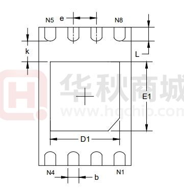
�PACKAGE INFORMATION
PACKAGE OUTLINE DIMENSIONS
TDFN-2×3-8L
D
N5
e
N8
k
L
E1
E
D1
N4
b
N1
BOTTOM VIEW
TOP VIEW
1.50
0.60
3.00
1.50
A
A1
A2
SIDE VIEW
0.25
0.50
RECOMMENDED LAND PATTERN (Unit: mm)
Symbol
Dimensions
In Millimeters
MIN
MAX
Dimensions
In Inches
MIN
MAX
A
0.700
0.800
0.028
0.031
A1
0.000
0.050
0.000
0.002
A2
0.203 REF
0.008 REF
D
1.924
2.076
0.076
0.082
D1
1.400
1.600
0.055
0.063
E
2.924
3.076
0.115
0.121
E1
1.400
1.600
0.055
0.063
k
b
0.200 MIN
0.200
e
L
0.008 MIN
0.300
0.008
0.376
0.009
0.500 TYP
0.224
0.012
0.020 TYP
0.015
NOTE: This drawing is subject to change without notice.
SG Micro Corp
www.sg-micro.com
TX00057.000
Downloaded From Oneyac.com
�PACKAGE INFORMATION
TAPE AND REEL INFORMATION
REEL DIMENSIONS
TAPE DIMENSIONS
P2
W
P0
Q1
Q2
Q1
Q2
Q1
Q2
Q3
Q4
Q3
Q4
Q3
Q4
B0
Reel Diameter
A0
P1
K0
Reel Width (W1)
DIRECTION OF FEED
NOTE: The picture is only for reference. Please make the object as the standard.
KEY PARAMETER LIST OF TAPE AND REEL
Reel
Diameter
Reel Width
W1
(mm)
A0
(mm)
B0
(mm)
K0
(mm)
P0
(mm)
P1
(mm)
P2
(mm)
W
(mm)
Pin1
Quadrant
TDFN-2×3-8L
7″
9.5
2.30
3.30
1.10
4.0
4.0
2.0
8.0
Q2
SG Micro Corp
www.sg-micro.com
TX10000.000
Downloaded From Oneyac.com
DD0001
Package Type
�PACKAGE INFORMATION
CARTON BOX DIMENSIONS
NOTE: The picture is only for reference. Please make the object as the standard.
KEY PARAMETER LIST OF CARTON BOX
Length
(mm)
Width
(mm)
Height
(mm)
Pizza/Carton
7″ (Option)
368
227
224
8
7″
442
410
224
18
SG Micro Corp
www.sg-micro.com
DD0002
Reel Type
TX20000.000
Downloaded From Oneyac.com
�单击下面可查看定价,库存,交付和生命周期等信息
>>SGMICRO(圣邦微电子)
Downloaded From Oneyac.com
�


 工商网监
湘ICP备2023018690号
工商网监
湘ICP备2023018690号
