GP1FMV51TK0F
GP1FMV51TK0F
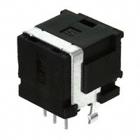
Fiber Optic Transmitter Square connector Compact (without mounting hole) With shutter
■Description
GP1FMV51TK0F has a built-in LED with a peak light emission wavelength of 660 nm and the associated drive IC, and the input is TTL level compatible.
■Agency approvals/Compliance
1. Compliant with JEITA RC-5720B and CP1201 2. Compliant with RoHS directive (2002/95/EC)
■Features
■Applications
1. Fiber optic transmitter (Receiver : GP1FMV51RK0F) 2. Square connector (JEITA RC-5720B) 3. Compact (without mounting hole) 4. With shutter function 5. Supply voltage : 5 V 6. Transfer rate : 13.2 Mb/s
1. AV equipment (DVD, CD, MD players etc.) 2. FPD-TV
Notice The content of data sheet is subject to change without prior notice. In the absence of confirmation by device specification sheets, SHARP takes no responsibility for any defects that may occur in equipment using any SHARP devices shown in catalogs, data books, etc. Contact SHARP in order to obtain the latest device specification sheets before using any SHARP device. Sheet No.: E2-A00201EN Date Dec.01.2006 ©SHARP Corporation
1
�GP1FMV51TK0F
■Outline Dimensions
[1]
Symbol A B C D Description Holder Shutter Fixing pin Lead pin
(Unit: mm)
Material PBT (Color : Black) PBT (Color : Black) SPCC (Lead free plating) Cu Alloy (SnCu plating)
[2]
(Lead root)
(Lead root)
Example of mounting drawing form solder side. PCB thickness t = 1.6 mm Unspecified tolerance ±0.1
Internal equivalent circuit
Pin arrangement
LED Driver IC
Vin Vcc GND
*1
*1 Input conditions of Vin terminal are designed to conform to TTL and CMOS. We recommend that the input fore Vin terminal uses the output of TTL and high speed CMOS.
[2] Portion marking
Production year (Last digit of production year) Production month Jan to Sep: 1 - 9 10 Oct: X 11 Nov: Y 12 Dec: Z Model Number
1) The connector joint area complies with the square connector JEITA RC-5720B 2) [1] portion : “S” mark, [2] portion : Model No. and date code shall be indicated. 3) Unspecified tolerance shall be ± 0.3. 4) Since there are other products which has a different fixing pin shape, please make sure to confirm reference mounting drawing for this device. 5) Dimensions in parenthesis are shown for reference.
5
1
T
Product mass : approx. 2 g
Sheet No.: E2-A00201EN
2
�GP1FMV51TK0F
■Absolute Maximum Ratings
Parameter Supply voltage Input voltage Operating temperature Storage temperature Soldering temperature *1 Symbol Rating VCC -0.5 to +7.0 Vin -05. to VCC+0.5 Topr -20 to +70 Tstg -30 to +80 260 Tsol 380 Unit Remark V V ℃ ℃ ℃ 6 s or less/time up to 2 times. 4 s or less/time up to 1 time. ℃ Soldering by hand at each terminal. *2
*1 Solder at a position more than 1.6 mm away from the base of the lead terminal. Reflow is not available. *2 Do not contact top of soldering iron to lead terminal directly.
■Recommended Operating Conditions
Parameter Supply voltage Operating transfer rate Symbol VCC T MIN. 4.75 TYP. 5.0 MAX. 5.25 13.2 Unit Remark V Mb/s NRZ signal duty 50%
■Electro-optical Characteristics
Parameter Symbol Conditions MIN. λp Peak emission wavelength 630 PC Output optical power couple into fiber Measurement method refer to Fig. 1 -21 ICC Supply current ViH Measurement method refer to Fig. 2 High level input voltage 2.0 ViL Low level input voltage tpLH L → H delay time → L delay time tpHL H Measurement method refer to Fig. 3, 4 Δtw Pulse width distortion -15 Δtj Jitter -
(Ta = 25 °C, VCC = 5 V) TYP. 660 -18 8 1 MAX. Unit 690 nm -15 dBm 13 mA V 0.8 V 180 ns 180 ns +15 ns 15 ns
Sheet No.: E2-A00201EN
3
�GP1FMV51TK0F
■Measurement Method
Fig. 1 Output Optical Power Coupled Into Fiber
Standard fiber optic cable GP1FMV51TK0F Device under test Optical power meter (Anritsu) ML93B
Vin
Vcc
GND Vcc D
The optical power meter must be calibrated to 660 nm. (0 dBm = 1 mW)
Notes 1. Vcc = 5.0 V (State of operating) 2. To bundle up the standard fiber optic cable, make it into a loop with the diameter D = 10 cm or more. (The standard fiber optic cable will be specified elsewhere.)
Fig. 2 Input Voltage and Supply Current
Standard fiber optic cable GP1FMV51TK0F Device under test Optical power meter (Anritsu) ML93B
Vin
Vcc Icc Vin
GND
The optical power meter must be calibrated to 660 nm. (0 dBm = 1 mW)
Vcc
Input conditions and judgment method
No. Input conditions 1 Vin = 2.0 V or more Vin = 0.8 V or less 2
Notes Vcc = 5.0 V (State of operating)
Judgment method -21 ≤ PC ≤ -15 dBm, ICC = 13 mA or less PC ≤ -36 dBm, ICC = 13 mA or less
Sheet No.: E2-A00201EN
4
�GP1FMV51TK0F Fig. 3 Pulse Response and Jitter
Standard fiber optic cable GP1FMV51TK0F Device under test Output signal
Standard receiver
Vin
Vcc Icc Vin
GND
Vcc Oscilloscope (band width: 1 GHz) Trigger: CH1 Mode: Storage mode
CH1 Input CH2
Oscilloscope
1
1
0
0
Input signal 6.6 Mb/s bi-phase PRBS signal
Fig. 4 Input Signal (6.6 Mb/s Bi-phase PRBS Signal)
Input signal 50%
tpLH
tpHL
Standard receiver output
50%
∆tjr
∆tjf
Notes (1) The wave form write time shall be 4 s. But do not allow the wave form to be distorted by increasing the brightness too much. (2) VCC = 5.0 V (State of operating) (3) The probe for the oscilloscope must be more than 1 MΩ and less than 10 pF.
Sheet No.: E2-A00201EN
5
�GP1FMV51TK0F
■Design and Production Notes
(1) Stabilization of power supply line Please put a by-pass capacitor (0.1 μF) close to the device at least within 7 mm of the terminal. Please also put a 4.7 μF capacitor across the power supply line nearby. (2) Soldering condition Solder at the condition within the absolute maximum ratings in this sheet. In case of using flow soldering, please make sure of the conditions of process at the flow equipment. Also, do not use reflow soldering. In case of soldering by hand, do not contact top of soldering iron to lead terminal directly. (Solder at a position more than 1.6 mm away from the base of the lead terminal.) (3) About getting dirt and dust in the connector coupling portion In case dirt or dust comes into the connector coupling portion, please use a blower to take it off. Any rigid rod-like object must not be inserted since into the coupling portion. The internal device might be damaged, resulting deteriorated characteristics. (4) Cleaning Do not immerse for cleaning. The solvent would get into the connector coupling portion resulting deteriorated characteristics. Should it be necessary to remove the flux, please use one of the following solvents only to be applied with a brush. Solvent : Isopropyl alcohol, Methyl alcohol (5) Ground during assembling The human body and the soldering iron must be grounded against the static breakdown of the device during assembling. Please avoid touching the device terminals as much as possible before assembling. (6) Assembly of the device Please fix this device with soldering the metal sheet in PCB. And do not lay the PCB pattern or land for wiring where the metal sheet contacts PCB. (7) Input signal This product is designed intentionally based upon the signal transmission which is defined by the digital audio interface standard ; CP1201. When a signal out of JEITA standard CP-1201 is inputted to this device, there might be a case that this device can not transmit a signal correctly to receiving unit. (8) Fixing pin Since there are other products which has a different fixing pin shape, please make sure to confirm reference mounting drawing for this device. (9) Damage to connector coupling portion Please do not stress the connector coupling portion excessively since there might be a case that the shutter can’t operate normally. (10) About getting the flux into connector coupling portion Please avoid getting a flux into connector coupling portion of this device, because there might be a case that the characteristics deteriorate the shutter can’t operate normally.
Sheet No.: E2-A00201EN
6
�GP1FMV51TK0F
●Presence of ODC etc.
This product shall not contain the following materials. And they are not used in the production process for this product. Regulation substances : CFCs, Halon, Carbon tetrachloride, 1.1.1-Trichloroethane (Methylchloroform) Specific brominated flame retardants such as the PBB and PBDE are not used in this product at all. This product shall not contain the following materials banned in the RoHS Directive (2002/95/EC). • Lead, Mercury, Cadmium, Hexavalent chromium, Polybrominated biphenyls (PBB), Polybrominated diphenyl ethers (PBDE).
■Packing Specifications
PRODUCT
TRAY
PRODUCT Cross section of tray
PACKING MATERIAL Tray : Polystyrene PACKING METHOD Each tray holds 200 pieces.
Sheet No.: E2-A00201EN
7
�GP1FMV51TK0F
■Important Notices
· The circuit application examples in this publication are provided to explain representative applications of SHARP devices and are not intended to guarantee any circuit design or license any intellectual property rights. SHARP takes no responsibility for any problems related to any intellectual property right of a third party resulting from the use of SHARP's devices. · Contact SHARP in order to obtain the latest device specification sheets before using any SHARP device. SHARP reserves the right to make changes in the specifications, characteristics, data, materials, structure, and other contents described herein at any time without notice in order to improve design or reliability. Manufacturing locations are also subject to change without notice. · Observe the following points when using any devices in this publication. SHARP takes no responsibility for damage caused by improper use of the devices which does not meet the conditions and absolute maximum ratings to be used specified in the relevant specification sheet nor meet the following conditions: (i) The devices in this publication are designed for use in general electronic equipment designs such as: --- Personal computers --- Office automation equipment --- Telecommunication equipment [terminal] --- Test and measurement equipment --- Industrial control --- Audio visual equipment --- Consumer electronics (ii) Measures such as fail-safe function and redundant design should be taken to ensure reliability and safety when SHARP devices are used for or in connection with equipment that requires higher reliability such as: --- Transportation control and safety equipment (i.e., aircraft, trains, automobiles, etc.) --- Traffic signals --- Gas leakage sensor breakers --- Alarm equipment --- Various safety devices, etc. (iii) SHARP devices shall not be used for or in connection with equipment that requires an extremely high level of reliability and safety such as: --- Space applications --- Telecommunication equipment [trunk lines] --- Nuclear power control equipment --- Medical and other life support equipment (e.g., scuba). · If the SHARP devices listed in this publication fall within the scope of strategic products described in the Foreign Exchange and Foreign Trade Law of Japan, it is necessary to obtain approval to export such SHARP devices. · This publication is the proprietary product of SHARP and is copyrighted, with all rights reserved. Under the copyright laws, no part of this publication may be reproduced or transmitted in any form or by any means, electronic or mechanical, for any purpose, in whole or in part, without the express written permission of SHARP. Express written permission is also required before any use of this publication may be made by a third party. · Contact and consult with a SHARP representative if there are any questions about the contents of this publication.
Sheet No.: E2-A00201EN
8
�


 工商网监
湘ICP备2023018690号
工商网监
湘ICP备2023018690号
