Preliminary data
HITFET®BSP 78
Smart Lowside Power Switch
Features • Logic Level Input • Input Protection (ESD) • Thermal shutdown with auto restart • Overload protection • Short circuit protection • Overvoltage protection
• Current limitation
Product Summary
Drain source voltage
V DS
40 50 3 500
V mΩ A mJ
On-state resistance Nominal load current Clamping energy
R DS(on) ID(Nom) EAS
• Analog driving possible
Application
• All kinds of resistive, inductive and capacitive loads in switching or linear applications • µC compatible power switch for 12 V and 24 V DC applications • Replaces electromechanical relays and discrete circuits
N channel vertical power FET in Smart SIPMOS® technology. Fully protected by embedded protection functions.
General Description
Pin 1 2 3 TAB
Symbol IN DRAIN SOURCE DRAIN
Function Input Output to the load Ground Output to the load
Semiconductor Group
Page 1
Jan-15-1998
�Preliminary data
BSP 78
Block Diagram
Vb b
+
LOAD
M
Drain
C u rrent lim i t a t i o n G a te-Driving Overvoltage protection
IN
U n it
ESD
Overload protection
Overtemperature protection
Short c rcu t S h o r t c ii r c u ii t p rro tte c ttiio n p o ec on
Source
H ITFET
®
Semiconductor Group
Page 2
Jan-15-1998
�Preliminary data Maximum Ratings at T j = 25°C, unless otherwise specified Parameter
Drain source voltage
BSP 78
Symbol
V DS
Value 40 40 -0.2 ... +10 -0.2 ... VDS -40 ...+150 -55 ...+150 1.7 500 2000
Unit V
Drain source voltage for short circuit protection Continuous input voltage Peak input voltage (IIN ≤ 2 mA)
Operating temperature Storage temperature
VDS(SC) VIN VIN(peak)
Tj Tstg P tot
°C W mJ kV
Power dissipation, TC = 85 °C Unclamped single pulse inductive energy F)
EAS
Electrostatic discharge voltage (Human Body Model) VESD according to MIL STD 883D, method 3015.7 and EOS/ESD assn. standard S5.1 - 1993
DIN humidity category, DIN 40 040
E 40/150/56
IEC climatic category; DIN IEC 68-1
Thermal resistance junction - ambient: @ min. footprint @ 6 cm2 cooling area F) junction-soldering point: R thJS
RthJA
K/W 125 72 17 K/W
1 not
tested, specified by design on 50mm+50mm*1.5mm epoxy PCB FR4 with 6 cm2 (one layer, 70µm thick) copper area for Drain connection. PCB is vertical without blown air.
2 Device
Semiconductor Group
Page 3
Jan-15-1998
�Preliminary data Electrical Characteristics Parameter at Tj = 25°C, unless otherwise specified Characteristics Drain source clamp voltage Tj = - 40 ...+ 150, Imess = 10 mA Off-state drain currentTj = -40 ... +150°C VIN = 0 V, VDS = 32 V Input treshold voltage ID = 0.7 mA On state input current On-state resistance ID = 3 A, VIN = 5 V, Tj = 25 °C ID = 3 A, VIN = 5 V, Tj = 150 °C On-state resistance ID = 3 A, VIN = 10 V, Tj = 25 °C ID = 3 A, VIN = 10 V, Tj = 150 °C Nominal load current
VDS = 0.5 V, TS = 85 °C, Tj < 150°C,
BSP 78
Symbol min. VDS(AZ) IDSS VIN(th) IIN(on) R DS(on) R DS(on) ID(Nom) 3 40 1.3 -
Values typ. 1.7 10 45 75 35 65 max. 55 10 2.2 30 60 120 50 100 -
Unit
V µA V µA mΩ
A
VIN = 10 V Current limit (active if VDS>2.5 V) VIN = 10 V, VDS = 12 V Dynamic Characteristics Turn-on time VIN to 90% ID: ton toff -dVDS /dton dVDS /dtoff 60 60 0.4 0.7 150 150 1 1 V/µs
µs
ID(lim)
16
24
32
A
RL = 5 Ω , VIN = 0 to 10 V, Vbb = 12 V Turn-off time VIN to 10% ID: RL = 5 Ω , VIN = 10 to 0 V, Vbb = 12 V Slew rate on 70 to 50% Vbb: RL = 5 Ω , VIN = 0 to 10 V, Vbb = 12 V Slew rate off 50 to 70% Vbb: RL = 5 Ω , VIN = 10 to 0 V, Vbb = 12 V
Semiconductor Group
Page 4
Jan-15-1998
�Preliminary data Electrical Characteristics Parameter at Tj = 25°C, unless otherwise specified Protection Functions Thermal overload trip temperature Thermal hysteresis Input current protection mode Unclamped single pulse inductive energy F) ID = 3 A, Tj = 25 °C, Vbb = 12 V ID = 3 A, Tj = 150 °C, Vbb = 12 V Tjt ∆Tjt IIN(Prot) EAS 500 300 150 165 10 300 Symbol min. Values typ. max.
BSP 78
Unit
°C K µA mJ
Inverse Diode
Continuous source drain voltage VIN = 0 V , -ID = 5*3 A, tP = 300 µs VSD 1.1 V
1 not
tested, specified by design
Semiconductor Group
Page 5
Jan-15-1998
�Preliminary data
BSP 78
Block diagram
Terms Inductive and overvoltage output clamp
Input circuit (ESD protection)
Short circuit behaviour
V
IN
Gate Drive Input
I
IN
t
I
D
t
Source/ Ground
Input is not designed for DC current > 2 mA
T t
j
Thermal hysteresis
t
Semiconductor Group
Page 6
Jan-15-1998
�Preliminary data Maximum allowable power dissipation Ptot = f(TC)
1.7 W 1.4
BSP 78
On-state resistance R ON = f(T j); I D=3A; V IN=10V
120
mΩ
100 9 RDS(on)0 80 max.
Ptot
1.2 1.0 0.8
70 60 50 typ.
0.6 0.4
40 30 20
0.2 10 0.0 -50 -25 0 25 50 75 100 °C 150 0 -40 -15 10 35 60 85 110 135 °C 185
TC
Tj
On-state resistance R ON = f(T j); ID=3A; V IN=5V
Typ. input threshold voltage VIN(th) = f(T j); ID=-; V DS=12V
2.0 V max.
mΩ
140
120
RDS(on)
110 100 90 80 70 60 50 40 30 20 10 0 -40 -15 10 35 60 85 110 135 °C 185 0.0 -50 -25 0 25 50 75 100 °C 150 0.5 0.8 typ. 1.0
VIN(th)1.5
1.2
0.2
Tj
Tj
Semiconductor Group
Page 7
Jan-15-1998
�Preliminary data Typ. transfer characteristics ID = f(VIN); VDS=12V; Tj=25°C
30
BSP 78
Typ. short circuit current ID(SC) = f(T j); VDS=12V Parameter: V IN
30
A
A
ID
20
ID
20
Vin=10V 15 15 5V
10
10
5
5
0
0
1
2
3
4
5
6
7
8
V
10
0 -40
-15
10
35
60
85
110 135 °C
185
VIN
Tj
Typ. output characteristic ID = f(VDS); Tj=25°C Parameter: V IN
35 10V A 7V
Typ. overload current ID(lim) = f(t), Vbb=12 V, no heatsink Parameter: Tjstart
40 A
-40°C
ID
25
6V 5V 4V
ID(lim)
30
25
20 20 15 15 10 Vin=3V 10 5 150°C 85°C 5 25°C
0
0
1
2
3
4
V
6
0 0.0
0.5
1.0
1.5
2.0
s t
3.0
VDS
Semiconductor Group
Page 8
Jan-15-1998
�Preliminary data Typ. off-state drain current IDSS = f(Tj)
10 µA 8
BSP 78
Transient thermal impendance ZthJC = f(tP) Parameter: D=t P/T
max. 10 2 K/W D=0.5 0.2 10 1 0.1 0.05 0.02 10 0
IDSS
ZthJA
7 6 5 4 3 2 1 0 -40 10 -2 typ. 10 -1
0.01
0
-15
10
35
60
85
110 135 °C
185
10 -3 -7 -6 -5 -4 -3 -2 -1 0 1 10 10 10 10 10 10 10 10 10
s 10
3
Tj
tP
Semiconductor Group
Page 9
Jan-15-1998
�Preliminary data
BSP 78
Package and ordering code
all dimensions in mm
Ordering code: Q67060-S7203-A2
Semiconductor Group
Page 10
Jan-15-1998
�
很抱歉,暂时无法提供与“BSP78”相匹配的价格&库存,您可以联系我们找货
免费人工找货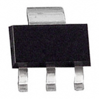


 工商网监
湘ICP备2023018690号
工商网监
湘ICP备2023018690号
