C8051F50x/F51x
Mixed Signal ISP Flash MCU Family
Analog Peripherals
- 12-Bit ADC
•
•
•
•
•
-
Memory
- 4352 bytes internal data RAM (256 + 4096 XRAM)
- 64 or 32 kB Flash; In-system programmable in
Up to 200 ksps
Up to 32 external single-ended inputs
VREF from on-chip VREF, external pin or VDD
Internal or external start of conversion source
Built-in temperature sensor
512-byte Sectors
Digital Peripherals
- 40, 33, or 25 Port I/O; All 5 V tolerant
- CAN 2.0 Controller—no crystal required
- LIN 2.1 Controller (Master and Slave capable); no
Two Comparators
•
•
•
Programmable hysteresis and response time
Configurable as interrupt or reset source
Low current
On-Chip Debug
- On-chip debug circuitry facilitates full speed, non-
-
intrusive in-system debug (no emulator required)
Provides breakpoints, single stepping,
inspect/modify memory and registers
Superior performance to emulation systems using
ICE-chips, target pods, and sockets
Low cost, complete development kit
-
-
Supply Voltage 1.8 to 5.25 V
- Typical operating current: 19 mA at 50 MHz;
- Typical stop mode current: 2 µA
High-Speed 8051 µC Core
- Pipelined instruction architecture; executes 70% of
-
ANALOG
PERIPHERALS
12-bit
200 ksps
ADC
Clock Sources
- Internal 24 MHz with ±0.5% accuracy for CAN and
-
master LIN operation
External oscillator: Crystal, RC, C, or clock
(1 or 2 pin modes)
Can switch between clock sources on-the-fly;
useful in power saving modes
Packages
- 48-Pin QFP/QFN (C8051F500/1/4/5)
- 40-Pin QFN (C8051F508/9-F510/1)
- 32-Pin QFP/QFN (C8051F502/3/6/7)
Automotive Qualified
- Temperature Range: –40 to +125 °C
- Compliant to AEC-Q100
instructions in 1 or 2 system clocks
Up to 50 MIPS throughput with 50 MHz clock
Expanded interrupt handler
A
M
U
X
crystal required
Hardware enhanced UART, SMBus™, and
enhanced SPI™ serial ports
Four general purpose 16-bit counter/timers
16-Bit programmable counter array (PCA) with six
capture/compare modules and enhanced PWM
functionality
TEMP
SENSOR
VREG
Voltage
Comparators 0-1 VREF
24 MHz PRECISION
INTERNAL OSCILLATOR
DIGITAL I/O
UART 0
SMBus
SPI
PCA
Timers 0-3
CAN
LIN
Ports 0-4
Crossbar
External
Memory
Interface
2x Clock Multiplier
HIGH-SPEED CONTROLLER CORE
64 kB
ISP FLASH
FLEXIBLE
INTERRUPTS
Rev. 1.2 3/11
8051 CPU
(50 MIPS)
DEBUG
CIRCUITRY
4 kB XRAM
POR
Copyright © 2011 by Silicon Laboratories
WDT
C8051F500/1/2/3/4/5/6/7/8/9-F510/1
�C8051F50x/F51x
2
Rev. 1.2
�C8051F50x/F51x
Table of Contents
1. System Overview ..................................................................................................... 16
2. Ordering Information ............................................................................................... 20
3. Pin Definitions.......................................................................................................... 22
4. Package Specifications ........................................................................................... 30
4.1. QFP-48 Package Specifications........................................................................ 30
4.2. QFN-48 Package Specifications........................................................................ 32
4.3. QFN-40 Package Specifications........................................................................ 34
4.4. QFP-32 Package Specifications........................................................................ 36
4.5. QFN-32 Package Specifications........................................................................ 38
5. Electrical Characteristics ........................................................................................ 40
5.1. Absolute Maximum Specifications..................................................................... 40
5.2. Electrical Characteristics ................................................................................... 41
6. 12-Bit ADC (ADC0) ................................................................................................... 52
6.1. Modes of Operation ........................................................................................... 53
6.1.1. Starting a Conversion................................................................................ 53
6.1.2. Tracking Modes......................................................................................... 53
6.1.3. Timing ....................................................................................................... 54
6.1.4. Burst Mode................................................................................................ 55
6.2. Output Code Formatting .................................................................................... 57
6.2.1. Settling Time Requirements...................................................................... 57
6.3. Selectable Gain ................................................................................................. 58
6.3.1. Calculating the Gain Value........................................................................ 58
6.3.2. Setting the Gain Value .............................................................................. 60
6.4. Programmable Window Detector....................................................................... 66
6.4.1. Window Detector In Single-Ended Mode .................................................. 68
6.5. ADC0 Analog Multiplexer .................................................................................. 70
7. Temperature Sensor ................................................................................................ 72
8. Voltage Reference.................................................................................................... 73
9. Comparators............................................................................................................. 75
9.1. Comparator Multiplexer ..................................................................................... 81
10. Voltage Regulator (REG0) ..................................................................................... 84
11. CIP-51 Microcontroller........................................................................................... 86
11.1. Performance .................................................................................................... 86
11.2. Instruction Set.................................................................................................. 88
11.2.1. Instruction and CPU Timing .................................................................... 88
11.3. CIP-51 Register Descriptions .......................................................................... 92
11.4. Serial Number Special Function Registers (SFRs) ......................................... 96
12. Memory Organization ............................................................................................ 97
12.1. Program Memory............................................................................................. 98
12.1.1. MOVX Instruction and Program Memory ................................................ 98
12.2. Data Memory ................................................................................................... 98
12.2.1. Internal RAM ........................................................................................... 98
12.2.1.1. General Purpose Registers ............................................................ 99
12.2.1.2. Bit Addressable Locations .............................................................. 99
Rev. 1.2
3
�C8051F50x/F51x
12.2.1.3. Stack ............................................................................................ 99
13. Special Function Registers................................................................................. 100
13.1. SFR Paging ................................................................................................... 100
13.2. Interrupts and SFR Paging ............................................................................ 100
13.3. SFR Page Stack Example ............................................................................. 101
14. Interrupts .............................................................................................................. 117
14.1. MCU Interrupt Sources and Vectors.............................................................. 117
14.1.1. Interrupt Priorities.................................................................................. 118
14.1.2. Interrupt Latency ................................................................................... 118
14.2. Interrupt Register Descriptions ...................................................................... 120
14.3. External Interrupts INT0 and INT1................................................................. 126
15. Flash Memory....................................................................................................... 129
15.1. Programming the Flash Memory ................................................................... 129
15.1.1. Flash Lock and Key Functions .............................................................. 129
15.1.2. Flash Erase Procedure ......................................................................... 129
15.1.3. Flash Write Procedure .......................................................................... 130
15.1.4. Flash Write Optimization ....................................................................... 130
15.2. Non-volatile Data Storage ............................................................................. 131
15.3. Security Options ............................................................................................ 131
15.4. Flash Write and Erase Guidelines ................................................................. 133
15.4.1. VDD Maintenance and the VDD monitor ................................................ 133
15.4.2. PSWE Maintenance .............................................................................. 133
15.4.3. System Clock ........................................................................................ 134
16. Power Management Modes................................................................................. 138
16.1. Idle Mode....................................................................................................... 138
16.2. Stop Mode ..................................................................................................... 139
16.3. Suspend Mode .............................................................................................. 139
17. Reset Sources ...................................................................................................... 141
17.1. Power-On Reset ............................................................................................ 142
17.2. Power-Fail Reset/VDD Monitor ..................................................................... 142
17.3. External Reset ............................................................................................... 144
17.4. Missing Clock Detector Reset ....................................................................... 144
17.5. Comparator0 Reset ....................................................................................... 145
17.6. PCA Watchdog Timer Reset ......................................................................... 145
17.7. Flash Error Reset .......................................................................................... 145
17.8. Software Reset .............................................................................................. 145
18. External Data Memory Interface and On-Chip XRAM ....................................... 147
18.1. Accessing XRAM........................................................................................... 147
18.1.1. 16-Bit MOVX Example .......................................................................... 147
18.1.2. 8-Bit MOVX Example ............................................................................ 147
18.2. Configuring the External Memory Interface ................................................... 148
18.3. Port Configuration.......................................................................................... 148
18.4. Multiplexed and Non-multiplexed Selection................................................... 153
18.4.1. Multiplexed Configuration...................................................................... 153
18.4.2. Non-multiplexed Configuration.............................................................. 154
4
Rev. 1.2
�C8051F50x/F51x
18.5. Memory Mode Selection................................................................................ 155
18.5.1. Internal XRAM Only .............................................................................. 155
18.5.2. Split Mode without Bank Select............................................................. 155
18.5.3. Split Mode with Bank Select.................................................................. 156
18.5.4. External Only......................................................................................... 156
18.6. Timing .......................................................................................................... 156
18.6.1. Non-Multiplexed Mode .......................................................................... 158
18.6.1.1. 16-bit MOVX: EMI0CF[4:2] = 101, 110, or 111............................. 158
18.6.1.2. 8-bit MOVX without Bank Select: EMI0CF[4:2] = 101 or 111 ....... 159
18.6.1.3. 8-bit MOVX with Bank Select: EMI0CF[4:2] = 110 ....................... 160
18.6.2. Multiplexed Mode .................................................................................. 161
18.6.2.1. 16-bit MOVX: EMI0CF[4:2] = 001, 010, or 011............................. 161
18.6.2.2. 8-bit MOVX without Bank Select: EMI0CF[4:2] = 001 or 011 ....... 162
18.6.2.3. 8-bit MOVX with Bank Select: EMI0CF[4:2] = 010 ....................... 163
19. Oscillators and Clock Selection ......................................................................... 165
19.1. System Clock Selection................................................................................. 165
19.2. Programmable Internal Oscillator .................................................................. 167
19.2.1. Internal Oscillator Suspend Mode ......................................................... 167
19.3. Clock Multiplier .............................................................................................. 170
19.4. External Oscillator Drive Circuit..................................................................... 172
19.4.1. External Crystal Example...................................................................... 174
19.4.2. External RC Example............................................................................ 175
19.4.3. External Capacitor Example.................................................................. 175
20. Port Input/Output ................................................................................................. 177
20.1. Port I/O Modes of Operation.......................................................................... 178
20.1.1. Port Pins Configured for Analog I/O...................................................... 178
20.1.2. Port Pins Configured For Digital I/O...................................................... 178
20.1.3. Interfacing Port I/O in a Multi-Voltage System ...................................... 179
20.2. Assigning Port I/O Pins to Analog and Digital Functions............................... 179
20.2.1. Assigning Port I/O Pins to Analog Functions ........................................ 179
20.2.2. Assigning Port I/O Pins to Digital Functions.......................................... 179
20.2.3. Assigning Port I/O Pins to External Digital Event Capture Functions ... 180
20.3. Priority Crossbar Decoder ............................................................................. 180
20.4. Port I/O Initialization ...................................................................................... 182
20.5. Port Match ..................................................................................................... 187
20.6. Special Function Registers for Accessing and Configuring Port I/O ............. 191
21. Local Interconnect Network (LIN)....................................................................... 201
21.1. Software Interface with the LIN Controller..................................................... 202
21.2. LIN Interface Setup and Operation................................................................ 202
21.2.1. Mode Definition ..................................................................................... 202
21.2.2. Baud Rate Options: Manual or Autobaud ............................................. 202
21.2.3. Baud Rate Calculations: Manual Mode................................................. 202
21.2.4. Baud Rate Calculations—Automatic Mode ........................................... 204
21.3. LIN Master Mode Operation .......................................................................... 205
21.4. LIN Slave Mode Operation ............................................................................ 206
Rev. 1.2
5
�C8051F50x/F51x
21.5. Sleep Mode and Wake-Up ............................................................................ 207
21.6. Error Detection and Handling ........................................................................ 207
21.7. LIN Registers................................................................................................. 208
21.7.1. LIN Direct Access SFR Registers Definitions ....................................... 208
21.7.2. LIN Indirect Access SFR Registers Definitions ..................................... 210
22. Controller Area Network (CAN0) ........................................................................ 218
22.1. Bosch CAN Controller Operation................................................................... 219
22.1.1. CAN Controller Timing .......................................................................... 219
22.1.2. CAN Register Access............................................................................ 220
22.1.3. Example Timing Calculation for 1 Mbit/Sec Communication ................ 220
22.2. CAN Registers............................................................................................... 222
22.2.1. CAN Controller Protocol Registers........................................................ 222
22.2.2. Message Object Interface Registers ..................................................... 222
22.2.3. Message Handler Registers.................................................................. 222
22.2.4. CAN Register Assignment .................................................................... 223
23. SMBus................................................................................................................... 226
23.1. Supporting Documents .................................................................................. 227
23.2. SMBus Configuration..................................................................................... 227
23.3. SMBus Operation .......................................................................................... 227
23.3.1. Transmitter vs. Receiver ....................................................................... 228
23.3.2. Arbitration.............................................................................................. 228
23.3.3. Clock Low Extension............................................................................. 228
23.3.4. SCL Low Timeout.................................................................................. 228
23.3.5. SCL High (SMBus Free) Timeout ......................................................... 229
23.4. Using the SMBus........................................................................................... 229
23.4.1. SMBus Configuration Register.............................................................. 229
23.4.2. SMB0CN Control Register .................................................................... 233
23.4.3. Data Register ........................................................................................ 236
23.5. SMBus Transfer Modes................................................................................. 236
23.5.1. Write Sequence (Master) ...................................................................... 237
23.5.2. Read Sequence (Master) ...................................................................... 238
23.5.3. Write Sequence (Slave) ........................................................................ 239
23.5.4. Read Sequence (Slave) ........................................................................ 240
23.6. SMBus Status Decoding................................................................................ 240
24. UART0 ................................................................................................................... 243
24.1. Baud Rate Generator .................................................................................... 243
24.2. Data Format................................................................................................... 245
24.3. Configuration and Operation ......................................................................... 246
24.3.1. Data Transmission ................................................................................ 246
24.3.2. Data Reception ..................................................................................... 246
24.3.3. Multiprocessor Communications ........................................................... 247
25. Enhanced Serial Peripheral Interface (SPI0) ..................................................... 252
25.1. Signal Descriptions........................................................................................ 253
25.1.1. Master Out, Slave In (MOSI)................................................................. 253
25.1.2. Master In, Slave Out (MISO)................................................................. 253
6
Rev. 1.2
�C8051F50x/F51x
25.1.3. Serial Clock (SCK) ................................................................................ 253
25.1.4. Slave Select (NSS) ............................................................................... 253
25.2. SPI0 Master Mode Operation ........................................................................ 254
25.3. SPI0 Slave Mode Operation .......................................................................... 256
25.4. SPI0 Interrupt Sources .................................................................................. 256
25.5. Serial Clock Phase and Polarity .................................................................... 257
25.6. SPI Special Function Registers ..................................................................... 258
26. Timers ................................................................................................................... 265
26.1. Timer 0 and Timer 1 ...................................................................................... 267
26.1.1. Mode 0: 13-bit Counter/Timer ............................................................... 267
26.1.2. Mode 1: 16-bit Counter/Timer ............................................................... 268
26.1.3. Mode 2: 8-bit Counter/Timer with Auto-Reload..................................... 268
26.1.4. Mode 3: Two 8-bit Counter/Timers (Timer 0 Only)................................ 269
26.2. Timer 2 .......................................................................................................... 275
26.2.1. 16-bit Timer with Auto-Reload............................................................... 275
26.2.2. 8-bit Timers with Auto-Reload............................................................... 275
26.2.3. External Oscillator Capture Mode ......................................................... 276
26.3. Timer 3 .......................................................................................................... 281
26.3.1. 16-bit Timer with Auto-Reload............................................................... 281
26.3.2. 8-bit Timers with Auto-Reload............................................................... 281
26.3.3. External Oscillator Capture Mode ......................................................... 282
27. Programmable Counter Array............................................................................. 287
27.1. PCA Counter/Timer ....................................................................................... 288
27.2. PCA0 Interrupt Sources................................................................................. 289
27.3. Capture/Compare Modules ........................................................................... 289
27.3.1. Edge-triggered Capture Mode............................................................... 290
27.3.2. Software Timer (Compare) Mode.......................................................... 291
27.3.3. High-Speed Output Mode ..................................................................... 292
27.3.4. Frequency Output Mode ....................................................................... 293
27.3.5. 8-bit, 9-bit, 10-bit and 11-bit Pulse Width Modulator Modes ................. 294
27.3.5.1. 8-bit Pulse Width Modulator Mode................................................ 294
27.3.5.2. 9/10/11-bit Pulse Width Modulator Mode...................................... 295
27.3.6. 16-Bit Pulse Width Modulator Mode...................................................... 296
27.4. Watchdog Timer Mode .................................................................................. 297
27.4.1. Watchdog Timer Operation ................................................................... 297
27.4.2. Watchdog Timer Usage ........................................................................ 298
27.5. Register Descriptions for PCA0..................................................................... 300
28. C2 Interface .......................................................................................................... 306
28.1. C2 Interface Registers................................................................................... 306
28.2. C2 Pin Sharing .............................................................................................. 309
Document Change List.............................................................................................. 310
Contact Information................................................................................................... 312
Rev. 1.2
7
�C8051F50x/F51x
List of Figures
Figure 1.1. C8051F500/1/4/5 Block Diagram .......................................................... 17
Figure 1.2. C8051F508/9-F510/1 Block Diagram .................................................... 18
Figure 1.3. C8051F502/3/6/7 Block Diagram .......................................................... 19
Figure 3.1. QFP-48 Pinout Diagram (Top View) ...................................................... 25
Figure 3.2. QFN-48 Pinout Diagram (Top View) ..................................................... 26
Figure 3.3. QFN-40 Pinout Diagram (Top View) ..................................................... 27
Figure 3.4. QFP-32 Pinout Diagram (Top View) ...................................................... 28
Figure 3.5. QFN-32 Pinout Diagram (Top View) ..................................................... 29
Figure 4.1. QFP-48 Package Drawing ..................................................................... 30
Figure 4.2. QFP-48 Landing Diagram ..................................................................... 31
Figure 4.3. QFN-48 Package Drawing .................................................................... 32
Figure 4.4. QFN-48 Landing Diagram ..................................................................... 33
Figure 4.5. Typical QFN-40 Package Drawing ........................................................ 34
Figure 4.6. QFN-40 Landing Diagram ..................................................................... 35
Figure 4.7. QFP-32 Package Drawing ..................................................................... 36
Figure 4.8. QFP-32 Package Drawing ..................................................................... 37
Figure 4.9. QFN-32 Package Drawing .................................................................... 38
Figure 4.10. QFN-32 Package Drawing .................................................................. 39
Figure 5.1. Minimum VDD Monitor Threshold vs. System Clock Frequency ........... 44
Figure 6.1. ADC0 Functional Block Diagram ........................................................... 52
Figure 6.2. ADC0 Tracking Modes .......................................................................... 54
Figure 6.3. 12-Bit ADC Tracking Mode Example ..................................................... 55
Figure 6.4. 12-Bit ADC Burst Mode Example With Repeat Count Set to 4 ............. 56
Figure 6.5. ADC0 Equivalent Input Circuit ............................................................... 58
Figure 6.6. ADC Window Compare Example: Right-Justified Data ......................... 69
Figure 6.7. ADC Window Compare Example: Left-Justified Data ........................... 69
Figure 6.8. ADC0 Multiplexer Block Diagram .......................................................... 70
Figure 7.1. Temperature Sensor Transfer Function ................................................ 72
Figure 8.1. Voltage Reference Functional Block Diagram ....................................... 73
Figure 9.1. Comparator Functional Block Diagram ................................................. 75
Figure 9.2. Comparator Hysteresis Plot .................................................................. 76
Figure 9.3. Comparator Input Multiplexer Block Diagram ........................................ 81
Figure 10.1. External Capacitors for Voltage Regulator Input/Output—
Regulator Enabled .............................................................................. 84
Figure 10.2. External Capacitors for Voltage Regulator Input/Output—
Regulator Disabled ............................................................................. 85
Figure 11.1. CIP-51 Block Diagram ......................................................................... 87
Figure 12.1. C8051F50x-F51x Memory Map ........................................................... 97
Figure 12.2. Flash Program Memory Map ............................................................... 98
Figure 13.1. SFR Page Stack ................................................................................ 101
Figure 13.2. SFR Page Stack While Using SFR Page 0x0 To Access SPI0DAT . 102
Figure 13.3. SFR Page Stack After CAN0 Interrupt Occurs .................................. 103
Figure 13.4. SFR Page Stack Upon PCA Interrupt Occurring During a CAN0 ISR 104
Rev. 1.2
8
�C8051F50x/F51x
Figure 13.5. SFR Page Stack Upon Return From PCA Interrupt .......................... 105
Figure 13.6. SFR Page Stack Upon Return From CAN0 Interrupt ........................ 106
Figure 15.1. Flash Program Memory Map ............................................................. 131
Figure 17.1. Reset Sources ................................................................................... 141
Figure 17.2. Power-On and VDD Monitor Reset Timing ....................................... 142
Figure 18.1. Multiplexed Configuration Example ................................................... 153
Figure 18.2. Non-multiplexed Configuration Example ........................................... 154
Figure 18.3. EMIF Operating Modes ..................................................................... 155
Figure 18.4. Non-multiplexed 16-bit MOVX Timing ............................................... 158
Figure 18.5. Non-multiplexed 8-bit MOVX without Bank Select Timing ................ 159
Figure 18.6. Non-multiplexed 8-bit MOVX with Bank Select Timing ..................... 160
Figure 18.7. Multiplexed 16-bit MOVX Timing ....................................................... 161
Figure 18.8. Multiplexed 8-bit MOVX without Bank Select Timing ........................ 162
Figure 18.9. Multiplexed 8-bit MOVX with Bank Select Timing ............................. 163
Figure 19.1. Oscillator Options .............................................................................. 165
Figure 19.2. Example Clock Multiplier Output ....................................................... 170
Figure 19.3. External 32.768 kHz Quartz Crystal Oscillator Connection Diagram 175
Figure 20.1. Port I/O Functional Block Diagram .................................................... 177
Figure 20.2. Port I/O Cell Block Diagram .............................................................. 178
Figure 20.3. Peripheral Availability on Port I/O Pins .............................................. 181
Figure 20.4. Crossbar Priority Decoder in Example Configuration ........................ 182
Figure 21.1. LIN Block Diagram ............................................................................ 201
Figure 22.1. Typical CAN Bus Configuration ......................................................... 218
Figure 22.2. CAN Controller Diagram .................................................................... 219
Figure 22.3. Four segments of a CAN Bit .............................................................. 221
Figure 23.1. SMBus Block Diagram ...................................................................... 226
Figure 23.2. Typical SMBus Configuration ............................................................ 227
Figure 23.3. SMBus Transaction ........................................................................... 228
Figure 23.4. Typical SMBus SCL Generation ........................................................ 230
Figure 23.5. Typical Master Write Sequence ........................................................ 237
Figure 23.6. Typical Master Read Sequence ........................................................ 238
Figure 23.7. Typical Slave Write Sequence .......................................................... 239
Figure 23.8. Typical Slave Read Sequence .......................................................... 240
Figure 24.1. UART0 Block Diagram ...................................................................... 243
Figure 24.2. UART0 Timing Without Parity or Extra Bit ......................................... 245
Figure 24.3. UART0 Timing With Parity ................................................................ 245
Figure 24.4. UART0 Timing With Extra Bit ............................................................ 245
Figure 24.5. Typical UART Interconnect Diagram ................................................. 246
Figure 24.6. UART Multi-Processor Mode Interconnect Diagram ......................... 247
Figure 25.1. SPI Block Diagram ............................................................................ 252
Figure 25.2. Multiple-Master Mode Connection Diagram ...................................... 255
Figure 25.3. 3-Wire Single Master and 3-Wire Single Slave Mode
Connection Diagram ......................................................................... 255
Figure 25.4. 4-Wire Single Master Mode and 4-Wire Slave Mode
Connection Diagram ......................................................................... 255
9
Rev. 1.2
�C8051F50x/F51x
Figure 25.5. Master Mode Data/Clock Timing ....................................................... 257
Figure 25.6. Slave Mode Data/Clock Timing (CKPHA = 0) ................................... 258
Figure 25.7. Slave Mode Data/Clock Timing (CKPHA = 1) ................................... 258
Figure 25.8. SPI Master Timing (CKPHA = 0) ....................................................... 262
Figure 25.9. SPI Master Timing (CKPHA = 1) ....................................................... 262
Figure 25.10. SPI Slave Timing (CKPHA = 0) ....................................................... 263
Figure 25.11. SPI Slave Timing (CKPHA = 1) ....................................................... 263
Figure 26.1. T0 Mode 0 Block Diagram ................................................................. 268
Figure 26.2. T0 Mode 2 Block Diagram ................................................................. 269
Figure 26.3. T0 Mode 3 Block Diagram ................................................................. 270
Figure 26.4. Timer 2 16-Bit Mode Block Diagram ................................................. 275
Figure 26.5. Timer 2 8-Bit Mode Block Diagram ................................................... 276
Figure 26.6. Timer 2 External Oscillator Capture Mode Block Diagram ................ 277
Figure 26.7. Timer 3 16-Bit Mode Block Diagram ................................................. 281
Figure 26.8. Timer 3 8-Bit Mode Block Diagram ................................................... 282
Figure 26.9. Timer 3 External Oscillator Capture Mode Block Diagram ................ 283
Figure 27.1. PCA Block Diagram ........................................................................... 287
Figure 27.2. PCA Counter/Timer Block Diagram ................................................... 288
Figure 27.3. PCA Interrupt Block Diagram ............................................................ 289
Figure 27.4. PCA Capture Mode Diagram ............................................................. 291
Figure 27.5. PCA Software Timer Mode Diagram ................................................. 292
Figure 27.6. PCA High-Speed Output Mode Diagram ........................................... 293
Figure 27.7. PCA Frequency Output Mode ........................................................... 294
Figure 27.8. PCA 8-Bit PWM Mode Diagram ........................................................ 295
Figure 27.9. PCA 9, 10 and 11-Bit PWM Mode Diagram ...................................... 296
Figure 27.10. PCA 16-Bit PWM Mode ................................................................... 297
Figure 27.11. PCA Module 2 with Watchdog Timer Enabled ................................ 298
Figure 28.1. Typical C2 Pin Sharing ...................................................................... 309
Rev. 1.2
10
�C8051F50x/F51x
List of Tables
Table 2.1. Product Selection Guide ......................................................................... 21
Table 3.1. Pin Definitions for the C8051F50x-F51x ................................................. 22
Table 4.1. QFP-48 Package Dimensions ................................................................ 30
Table 4.2. QFP-48 Landing Diagram Dimensions ................................................... 31
Table 4.3. QFN-48 Package Dimensions ................................................................ 32
Table 4.4. QFN-48 Landing Diagram Dimensions ................................................... 33
Table 4.5. QFN-40 Package Dimensions ................................................................ 34
Table 4.6. QFN-40 Landing Diagram Dimensions ................................................... 35
Table 4.7. QFP-32 Package Dimensions ................................................................ 36
Table 4.8. QFP-32 Landing Diagram Dimensions ................................................... 37
Table 4.9. QFN-32 Package Dimensions ................................................................ 38
Table 4.10. QFN-32 Landing Diagram Dimensions ................................................. 39
Table 5.1. Absolute Maximum Ratings .................................................................... 40
Table 5.2. Global Electrical Characteristics ............................................................. 41
Table 5.3. Port I/O DC Electrical Characteristics ..................................................... 45
Table 5.4. Reset Electrical Characteristics .............................................................. 46
Table 5.5. Flash Electrical Characteristics .............................................................. 46
Table 5.6. Internal High-Frequency Oscillator Electrical Characteristics ................. 47
Table 5.7. Clock Multiplier Electrical Specifications ................................................ 48
Table 5.8. Voltage Regulator Electrical Characteristics .......................................... 48
Table 5.9. ADC0 Electrical Characteristics .............................................................. 49
Table 5.10. Temperature Sensor Electrical Characteristics .................................... 50
Table 5.11. Voltage Reference Electrical Characteristics ....................................... 50
Table 5.12. Comparator 0 and Comparator 1 Electrical Characteristics ................. 51
Table 11.1. CIP-51 Instruction Set Summary (Prefetch-Enabled) ........................... 89
Table 13.1. Special Function Register (SFR) Memory Map for
Pages 0x0 and 0xF ............................................................................. 111
Table 13.2. Special Function Register (SFR) Memory Map for Page 0xC ............ 112
Table 13.3. Special Function Registers ................................................................. 113
Table 14.1. Interrupt Summary .............................................................................. 119
Table 15.1. Flash Security Summary .................................................................... 132
Table 18.1. EMIF Pinout (C8051F500/1/4/5) ......................................................... 149
Table 18.2. EMIF Pinout (C8051F508/9-F510/1) .................................................. 150
Table 18.3. AC Parameters for External Memory Interface ................................... 164
Table 20.1. Port I/O Assignment for Analog Functions ......................................... 179
Table 20.2. Port I/O Assignment for Digital Functions ........................................... 179
Table 20.3. Port I/O Assignment for External Digital Event Capture Functions .... 180
Table 21.1. Baud Rate Calculation Variable Ranges ............................................ 202
Table 21.2. Manual Baud Rate Parameters Examples ......................................... 204
Rev. 1.2
11
�C8051F50x/F51x
Table 21.3. Autobaud Parameters Examples ........................................................ 205
Table 21.4. LIN Registers (Indirectly Addressable) ............................................... 210
Table 22.1. Background System Information ........................................................ 220
Table 22.2. Standard CAN Registers and Reset Values ....................................... 223
Table 23.1. SMBus Clock Source Selection .......................................................... 230
Table 23.2. Minimum SDA Setup and Hold Times ................................................ 231
Table 23.3. Sources for Hardware Changes to SMB0CN ..................................... 235
Table 23.4. SMBus Status Decoding ..................................................................... 241
Table 24.1. Baud Rate Generator Settings for Standard Baud Rates ................... 244
Table 25.1. SPI Slave Timing Parameters ............................................................ 264
Table 27.1. PCA Timebase Input Options ............................................................. 288
Table 27.2. PCA0CPM and PCA0PWM Bit Settings for
PCA Capture/Compare Modules ........................................................ 290
Table 27.3. Watchdog Timer Timeout Intervals1 ................................................... 299
12
Rev. 1.2
�C8051F50x/F51x
List of Registers
SFR Definition 6.4. ADC0CF: ADC0 Configuration ...................................................... 63
SFR Definition 6.5. ADC0H: ADC0 Data Word MSB .................................................... 64
SFR Definition 6.6. ADC0L: ADC0 Data Word LSB ...................................................... 64
SFR Definition 6.7. ADC0CN: ADC0 Control ................................................................ 65
SFR Definition 6.8. ADC0TK: ADC0 Tracking Mode Select ......................................... 66
SFR Definition 6.9. ADC0GTH: ADC0 Greater-Than Data High Byte .......................... 67
SFR Definition 6.10. ADC0GTL: ADC0 Greater-Than Data Low Byte .......................... 67
SFR Definition 6.11. ADC0LTH: ADC0 Less-Than Data High Byte .............................. 68
SFR Definition 6.12. ADC0LTL: ADC0 Less-Than Data Low Byte ............................... 68
SFR Definition 6.13. ADC0MX: ADC0 Channel Select ................................................. 71
SFR Definition 8.1. REF0CN: Reference Control ......................................................... 74
SFR Definition 9.1. CPT0CN: Comparator0 Control ..................................................... 77
SFR Definition 9.2. CPT0MD: Comparator0 Mode Selection ....................................... 78
SFR Definition 9.3. CPT1CN: Comparator1 Control ..................................................... 79
SFR Definition 9.4. CPT1MD: Comparator1 Mode Selection ....................................... 80
SFR Definition 9.5. CPT0MX: Comparator0 MUX Selection ........................................ 82
SFR Definition 9.6. CPT1MX: Comparator1 MUX Selection ........................................ 83
SFR Definition 10.1. REG0CN: Regulator Control ........................................................ 85
SFR Definition 11.1. DPL: Data Pointer Low Byte ........................................................ 93
SFR Definition 11.2. DPH: Data Pointer High Byte ....................................................... 93
SFR Definition 11.3. SP: Stack Pointer ......................................................................... 94
SFR Definition 11.4. ACC: Accumulator ....................................................................... 94
SFR Definition 11.5. B: B Register ................................................................................ 94
SFR Definition 11.6. PSW: Program Status Word ........................................................ 95
SFR Definition 11.7. SNn: Serial Number n .................................................................. 96
SFR Definition 13.1. SFR0CN: SFR Page Control ..................................................... 107
SFR Definition 13.2. SFRPAGE: SFR Page ............................................................... 108
SFR Definition 13.3. SFRNEXT: SFR Next ................................................................ 109
SFR Definition 13.4. SFRLAST: SFR Last .................................................................. 110
SFR Definition 14.1. IE: Interrupt Enable .................................................................... 121
SFR Definition 14.2. IP: Interrupt Priority .................................................................... 122
SFR Definition 14.3. EIE1: Extended Interrupt Enable 1 ............................................ 123
SFR Definition 14.4. EIP1: Extended Interrupt Priority 1 ............................................ 124
SFR Definition 14.5. EIE2: Extended Interrupt Enable 2 ............................................ 125
SFR Definition 14.6. EIP2: Extended Interrupt Priority Enabled 2 .............................. 126
SFR Definition 14.7. IT01CF: INT0/INT1 Configuration .............................................. 128
SFR Definition 15.1. PSCTL: Program Store R/W Control ......................................... 134
SFR Definition 15.2. FLKEY: Flash Lock and Key ...................................................... 135
SFR Definition 15.3. FLSCL: Flash Scale ................................................................... 136
SFR Definition 15.4. CCH0CN: Cache Control ........................................................... 137
SFR Definition 15.5. ONESHOT: Flash Oneshot Period ............................................ 137
SFR Definition 16.1. PCON: Power Control ................................................................ 140
SFR Definition 17.1. VDM0CN: VDD Monitor Control ................................................ 144
Rev. 1.2
13
�C8051F50x/F51x
SFR Definition 17.2. RSTSRC: Reset Source ............................................................ 146
SFR Definition 18.1. EMI0CN: External Memory Interface Control ............................ 151
SFR Definition 18.2. EMI0CF: External Memory Configuration .................................. 152
SFR Definition 18.3. EMI0TC: External Memory Timing Control ................................ 157
SFR Definition 19.1. CLKSEL: Clock Select ............................................................... 166
SFR Definition 19.2. OSCICN: Internal Oscillator Control .......................................... 168
SFR Definition 19.3. OSCICRS: Internal Oscillator Coarse Calibration ...................... 169
SFR Definition 19.4. OSCIFIN: Internal Oscillator Fine Calibration ............................ 169
SFR Definition 19.5. CLKMUL: Clock Multiplier .......................................................... 171
SFR Definition 19.6. OSCXCN: External Oscillator Control ........................................ 173
SFR Definition 20.1. XBR0: Port I/O Crossbar Register 0 .......................................... 184
SFR Definition 20.2. XBR1: Port I/O Crossbar Register 1 .......................................... 185
SFR Definition 20.3. XBR2: Port I/O Crossbar Register 1 .......................................... 186
SFR Definition 20.4. P0MASK: Port 0 Mask Register ................................................. 187
SFR Definition 20.5. P0MAT: Port 0 Match Register .................................................. 187
SFR Definition 20.6. P1MASK: Port 1 Mask Register ................................................. 188
SFR Definition 20.7. P1MAT: Port 1 Match Register .................................................. 188
SFR Definition 20.8. P2MASK: Port 2 Mask Register ................................................. 189
SFR Definition 20.9. P2MAT: Port 2 Match Register .................................................. 189
SFR Definition 20.10. P3MASK: Port 3 Mask Register ............................................... 190
SFR Definition 20.11. P3MAT: Port 3 Match Register ................................................ 190
SFR Definition 20.12. P0: Port 0 ................................................................................. 191
SFR Definition 20.13. P0MDIN: Port 0 Input Mode ..................................................... 192
SFR Definition 20.14. P0MDOUT: Port 0 Output Mode .............................................. 192
SFR Definition 20.15. P0SKIP: Port 0 Skip ................................................................. 193
SFR Definition 20.16. P1: Port 1 ................................................................................. 193
SFR Definition 20.17. P1MDIN: Port 1 Input Mode ..................................................... 194
SFR Definition 20.18. P1MDOUT: Port 1 Output Mode .............................................. 194
SFR Definition 20.19. P1SKIP: Port 1 Skip ................................................................. 195
SFR Definition 20.20. P2: Port 2 ................................................................................. 195
SFR Definition 20.21. P2MDIN: Port 2 Input Mode ..................................................... 196
SFR Definition 20.22. P2MDOUT: Port 2 Output Mode .............................................. 196
SFR Definition 20.23. P2SKIP: Port 2 Skip ................................................................. 197
SFR Definition 20.24. P3: Port 3 ................................................................................. 197
SFR Definition 20.25. P3MDIN: Port 3 Input Mode ..................................................... 198
SFR Definition 20.26. P3MDOUT: Port 3 Output Mode .............................................. 198
SFR Definition 20.27. P3SKIP: Port 3Skip .................................................................. 199
SFR Definition 20.28. P4: Port 4 ................................................................................. 199
SFR Definition 20.29. P4MDOUT: Port 4 Output Mode .............................................. 200
SFR Definition 21.1. LIN0ADR: LIN0 Indirect Address Register ................................. 208
SFR Definition 21.2. LIN0DAT: LIN0 Indirect Data Register ....................................... 208
SFR Definition 21.3. LIN0CF: LIN0 Control Mode Register ........................................ 209
SFR Definition 22.1. CAN0CFG: CAN Clock Configuration ........................................ 225
SFR Definition 23.1. SMB0CF: SMBus Clock/Configuration ...................................... 232
SFR Definition 23.2. SMB0CN: SMBus Control .......................................................... 234
14
Rev. 1.2
�C8051F50x/F51x
SFR Definition 23.3. SMB0DAT: SMBus Data ............................................................ 236
SFR Definition 24.1. SCON0: Serial Port 0 Control .................................................... 248
SFR Definition 24.2. SMOD0: Serial Port 0 Control .................................................... 249
SFR Definition 24.3. SBUF0: Serial (UART0) Port Data Buffer .................................. 250
SFR Definition 24.4. SBCON0: UART0 Baud Rate Generator Control ...................... 250
SFR Definition 24.6. SBRLL0: UART0 Baud Rate Generator Reload Low Byte ........ 251
SFR Definition 24.5. SBRLH0: UART0 Baud Rate Generator Reload High Byte ....... 251
SFR Definition 25.1. SPI0CFG: SPI0 Configuration ................................................... 259
SFR Definition 25.2. SPI0CN: SPI0 Control ............................................................... 260
SFR Definition 25.3. SPI0CKR: SPI0 Clock Rate ....................................................... 261
SFR Definition 25.4. SPI0DAT: SPI0 Data ................................................................. 261
SFR Definition 26.1. CKCON: Clock Control .............................................................. 266
SFR Definition 26.2. TCON: Timer Control ................................................................. 271
SFR Definition 26.3. TMOD: Timer Mode ................................................................... 272
SFR Definition 26.4. TL0: Timer 0 Low Byte ............................................................... 273
SFR Definition 26.5. TL1: Timer 1 Low Byte ............................................................... 273
SFR Definition 26.6. TH0: Timer 0 High Byte ............................................................. 274
SFR Definition 26.7. TH1: Timer 1 High Byte ............................................................. 274
SFR Definition 26.8. TMR2CN: Timer 2 Control ......................................................... 278
SFR Definition 26.9. TMR2RLL: Timer 2 Reload Register Low Byte .......................... 279
SFR Definition 26.10. TMR2RLH: Timer 2 Reload Register High Byte ...................... 279
SFR Definition 26.11. TMR2L: Timer 2 Low Byte ....................................................... 280
SFR Definition 26.12. TMR2H Timer 2 High Byte ....................................................... 280
SFR Definition 26.13. TMR3CN: Timer 3 Control ....................................................... 284
SFR Definition 26.14. TMR3RLL: Timer 3 Reload Register Low Byte ........................ 285
SFR Definition 26.15. TMR3RLH: Timer 3 Reload Register High Byte ...................... 285
SFR Definition 26.16. TMR3L: Timer 3 Low Byte ....................................................... 286
SFR Definition 26.17. TMR3H Timer 3 High Byte ....................................................... 286
SFR Definition 27.1. PCA0CN: PCA Control .............................................................. 300
SFR Definition 27.2. PCA0MD: PCA Mode ................................................................ 301
SFR Definition 27.3. PCA0PWM: PCA PWM Configuration ....................................... 302
SFR Definition 27.4. PCA0CPMn: PCA Capture/Compare Mode .............................. 303
SFR Definition 27.5. PCA0L: PCA Counter/Timer Low Byte ...................................... 304
SFR Definition 27.6. PCA0H: PCA Counter/Timer High Byte ..................................... 304
SFR Definition 27.7. PCA0CPLn: PCA Capture Module Low Byte ............................. 305
SFR Definition 27.8. PCA0CPHn: PCA Capture Module High Byte ........................... 305
C2 Register Definition 28.1. C2ADD: C2 Address ...................................................... 306
C2 Register Definition 28.2. DEVICEID: C2 Device ID ............................................... 307
C2 Register Definition 28.3. REVID: C2 Revision ID .................................................. 307
C2 Register Definition 28.4. FPCTL: C2 Flash Programming Control ........................ 308
C2 Register Definition 28.5. FPDAT: C2 Flash Programming Data ............................ 308
Rev. 1.2
15
�C8051F50x/F51x
1. System Overview
C8051F50x/F51x devices are fully integrated mixed-signal System-on-a-Chip MCUs. Highlighted features
are listed below. Refer to Table 2.1 for specific product feature selection and part ordering numbers.
High-speed pipelined 8051-compatible microcontroller core (up to 50 MIPS)
In-system, full-speed, non-intrusive debug interface (on-chip)
Controller Area Network (CAN 2.0B) Controller with 32 message objects, each with its own indentifier
mask (C8051F500/2/4/6/8-F510)
LIN 2.1 peripheral (fully backwards compatible, master and slave modes) (C8051F500/2/4/6/8-F510)
True 12-bit 200 ksps 32-channel single-ended ADC with analog multiplexer
Precision programmable 24 MHz internal oscillator that is within ±0.5% across the temperature range
and for VDD voltages greater than or equal to the on-chip voltage regulator minimum output at the low
setting. The oscillator is within +1.0% for VDD voltages below this minimum output setting.
On-chip Clock Multiplier to reach up to 50 MHz
64 kB (C8051F500/1/2/3/8/9) or 32 kB (C8051F504/5/6/7-F510/1) of on-chip Flash memory
4352 bytes of on-chip RAM
SMBus/I2C, Enhanced UART, and Enhanced SPI serial interfaces implemented in hardware
Four general-purpose 16-bit timers
External Data Memory Interface (C8051F500/1/4/5 and C8051F508/9-F510/1) with 64 kB address
space
Programmable Counter/Timer Array (PCA) with six capture/compare modules and Watchdog Timer
function
On-chip Voltage Regulator
On-chip Power-On Reset, VDD Monitor, and Temperature Sensor
On-chip Voltage Comparator
40, 33, or 25 Port I/O (5 V push-pull)
With on-chip Voltage Regulator, Power-On Reset, VDD monitor, Watchdog Timer, and clock oscillator, the
C8051F50x/F51x devices are truly stand-alone System-on-a-Chip solutions. The Flash memory can be
reprogrammed even in-circuit, providing non-volatile data storage, and also allowing field upgrades of the
8051 firmware. User software has complete control of all peripherals, and may individually shut down any
or all peripherals for power savings.
The on-chip Silicon Labs 2-Wire (C2) Development Interface allows non-intrusive (uses no on-chip
resources), full speed, in-circuit debugging using the production MCU installed in the final application. This
debug logic supports inspection and modification of memory and registers, setting breakpoints, single
stepping, run and halt commands. All analog and digital peripherals are fully functional while debugging
using C2. The two C2 interface pins can be shared with user functions, allowing in-system debugging without occupying package pins.
The devices are specified for 1.8 V to 5.25 V operation over the automotive temperature range (–40 to
+125 °C). The Port I/O and RST pins can interface to 5 V logic by setting the VIO pin to 5 V. The
C8051F500/1/4/5 devices are available in 48-pin QFP and QFN packages, the C8051F508/9-F510/1 are
available in 40-pin QFN packages, and the C8051F502/3/6/7 devices are available in 32-pin QFP and
QFN packages. All package options are lead-free and RoHS compliant. See Table 2.1 for ordering information. Block diagrams are included in Figure 1.1, Figure 1.2, and Figure 1.3.
Rev. 1.2
16
�C8051F50x/F51x
VIO
Power On
Reset
Reset
C2CK/RST
C2D
Debug /
Programming
Hardware
Port I/O Configuration
CIP-51 8051
Controller Core
up to 64kB Byte Flash
Program Memory
UART0
256 Byte RAM
Timers 0,
1, 2, 3
4 kB XRAM
PCA
WDT
Voltage Regulator
(LDO)
CAN 2.0B
SPI
VDD
Port 2
Drivers
P2.0
P2.1
P2.2
P2.3
P2.4
P2.5
P2.6
P2.7
Port 3
Drivers
P3.0
P3.1
P3.2
P3.3
P3.4
P3.5
P3.6
P3.7
Port 4
Drivers
P4.0
P4.1
P4.2
P4.3
P4.4
P4.5
P4.6
P4.7
I2C
GND
System Clock Setup
SFR
Bus
Internal Oscillator
Crossbar Control
External Memory Interface
*On F500/4 Devices
XTAL1 XTAL2
Analog Peripherals
External Oscillator
Voltage
Reference
Clock Multiplier
VDD
VREF
VREF
12-bit
200ksps
ADC
A
M
U
X
CP0, CP0A
VDDA
Comparator 0
VDD
VREF
P0 – P3
Temp
Sensor
GND
+
-
GNDA
CP1, CP1A
Comparator 1
+
-
Figure 1.1. C8051F500/1/4/5 Block Diagram
17
Port 1
Drivers
P1.0
P1.1
P1.2
P1.3
P1.4
P1.5
P1.6
P1.7
Priority
Crossbar
Decoder
LIN 2.1
VREGIN
Port 0
Drivers
P0.0
P0.1
P0.2
P0.3
P0.4
P0.5
P0.6
P0.7
Digital Peripherals
Rev. 1.2
�C8051F50x/F51x
VIO
Power On
Reset
Reset
C2CK/RST
Port I/O Configuration
CIP-51 8051
Controller Core
Debug /
Programming
Hardware
UART0
256 Byte RAM
Timers 0,
1, 2, 3
6 channel
PCA/WDT
4 kB XRAM
Port 1
Drivers
Port 2
Drivers
P2.0
P2.1
P2.2
P2.3
P2.4
P2.5
P2.6
P2.7
Port 3
Drivers
P3.0
P3.1
P3.2
P3.3
P3.4
P3.5
P3.6
P3.7
Priority
Crossbar
Decoder
LIN 2.1
VREGIN
P1.0
P1.1
P1.2
P1.3
P1.4
P1.5
P1.6
P1.7
Digital Peripherals
up to 64 kB Byte Flash
Program Memory
C2D
Port 0
Drivers
P0.0
P0.1
P0.2
P0.3
P0.4
P0.5
P0.6/
P0.7
Voltage Regulator
(LDO)
CAN 2.0B
SPI
VDD
I2C
GND
System Clock Setup
SFR
Bus
Crossbar Control
External Memory Interface
*On ‘F508-F510 devices
XTAL1 XTAL2
Internal Oscillator
External Oscillator
Analog Peripherals
Voltage
Reference
Clock Multiplier
VDD
VREF
12-bit
200ksps
ADC
VDDA
VREF
A
M
U
X
VDD
VREF
P0 – P3
Temp
Sensor
GND
CP0, CP0A
Comparator 0
+
-
CP1, CP1A
Comparator 1
+
-
Port 4
Driver
P4.0 / C2D
GNDA
Figure 1.2. C8051F508/9-F510/1 Block Diagram
Rev. 1.2
18
�C8051F50x/F51x
VIO
Power On
Reset
Reset
C2CK/RST
Debug /
Programming
Hardware
Port I/O Configuration
CIP-51 8051
Controller Core
up to 64kB Byte Flash
Program Memory
C2D
UART0
256 Byte RAM
Timers 0,
1, 2, 3
4 kB XRAM
PCA/
WDT
Port 1
Drivers
P1.0
P1.1
P1.2
P1.3
P1.4
P1.5
P1.6
P1.7
Port 2
Drivers
P2.0
P2.1
P2.2
P2.3
P2.4
P2.5
P2.6
P2.7
Priority
Crossbar
Decoder
LIN 2.1
VREGIN
Port 0
Drivers
P0.0
P0.1
P0.2
P0.3
P0.4
P0.5
P0.6
P0.7
Digital Peripherals
Voltage Regulator
(LDO)
CAN 2.0B
SPI
VDD
I2C
GND
System Clock Setup
SFR
Bus
Crossbar Control
*On F502/6 Devices
XTAL1 XTAL2
Internal Oscillator
Analog Peripherals
External Oscillator
Voltage
Reference
Clock Multiplier
VDD
VREF
VREF
12-bit
200ksps
ADC
A
M
U
X
CP0, CP0A
VDDA
Comparator 0
VDD
VREF
P0 – P3
Temp
Sensor
GND
+
-
GNDA
CP1, CP1A
Comparator 1
+
-
Figure 1.3. C8051F502/3/6/7 Block Diagram
19
Rev. 1.2
Port 3
Drivers
P3.0 / C2D
�C8051F50x/F51x
2. Ordering Information
The following features are common to all devices in this family:
50 MHz system clock and 50 MIPS throughput (peak)
4352 bytes of RAM (256 internal bytes and 4096 XRAM bytes)
SMBus/I2C, Enhanced SPI, Enhanced UART
Four Timers
Six Programmable Counter Array channels
Internal 24 MHz oscillator
Internal Voltage Regulator
12-bit, 200 ksps ADC
Internal Voltage Reference and Temperature Sensor
Two Analog Comparators
Table 2.1 shows the feature that differentiate the devices in this family.
Rev. 1.2
20
�C8051F50x/F51x
Package
External Memory Interface
Digital Port I/Os
LIN2.0
CAN2.0B
Flash Memory (kB)
Ordering Part Number
Package
External Memory Interface
Digital Port I/Os
LIN2.0
CAN2.0B
Flash Memory (kB)
Ordering Part Number
Table 2.1. Product Selection Guide
C8051F500-IQ 64
40
QFP-48 C8051F505-IQ 32
— — 40
QFP-48
C8051F500-IM 64
40
QFN-48 C8051F505-IM 32
— — 40
QFN-48
C8051F501-IQ 64
— —
40
QFP-48 C8051F506-IQ 32
25 —
QFP-32
C8051F501-IM 64
— —
40
QFN-48 C8051F506-IM 32
25 —
QFN-32
C8051F502-IQ 64
25 —
QFP-32 C8051F507-IQ 32
— — 25 —
QFP-32
C8051F502-IM 64
25 —
QFN-32 C8051F507-IM 32
— — 25 —
QFN-32
C8051F503-IQ 64
— —
25 —
QFP-32 C8051F508-IM 64
33
QFN-40
C8051F503-IM 64
— —
25 —
QFN-32 C8051F509-IM 64
— — 33
QFN-40
C8051F504-IQ 32
40
QFP-48 C8051F510-IM 32
33
QFN-40
C8051F504-IM 32
40
QFN-48 C8051F511-IM 32
— — 33
QFN-40
Note: The suffix of the part number indicates the device rating and the package. All devices are RoHS compliant.
All of these devices are also available in an automotive version. For the automotive version, the -I in the
ordering part number is replaced with -A. For example, the automotive version of the C8051F500-IM is the
C8051F500-AM.
The -AM and -AQ devices receive full automotive quality production status, including AEC-Q100 qualification, registration with International Material Data System (IMDS) and Part Production Approval Process
(PPAP) documentation. PPAP documentation is available at www.silabs.com with a registered and NDA
approved user account. The -AM and -AQ devices enable high volume automotive OEM applications with
their enhanced testing and processing. Please contact Silicon Labs sales for more information regarding
–AM and -AQ devices for your automotive project.
21
Rev. 1.2
�C8051F50x/F51x
3. Pin Definitions
Table 3.1. Pin Definitions for the C8051F50x/F51x
Name
Pin
‘F500/1/4/5
Pin
‘F502/3/6/7
(48-pin)
Pin
F508/9F510/1
(40-pin)
VDD
4
4
4
Digital Supply Voltage. Must be connected.
GND
6
6
6
Digital Ground. Must be connected.
VDDA
5
5
5
Analog Supply Voltage. Must be connected.
GNDA
7
7
7
Analog Ground. Must be connected.
VREGIN
3
3
3
Voltage Regulator Input
VIO
2
2
2
Port I/O Supply Voltage. Must be connected.
RST/
12
10
10
Type
Description
(32-pin)
C2CK
D I/O
Device Reset. Open-drain output of internal
POR or VDD Monitor. An external source
can initiate a system reset by driving this pin
low.
D I/O
Clock signal for the C2 Debug Interface.
Bi-directional data signal for the C2 Debug
Interface.
C2D
11
—
—
D I/O
P4.0/
—
9
—
D I/O or A In Port 4.0. See SFR Definition 20.29 for a
description.
C2D
P3.0/
Bi-directional data signal for the C2 Debug
Interface.
D I/O
—
9
C2D
D I/O or A In Port 3.0. See SFR Definition 20.24 for a
description.
Bi-directional data signal for the C2 Debug
Interface.
D I/O
P0.0
8
8
8
D I/O or A In Port 0.0. See SFR Definition 20.12 for a
description.
P0.1
1
1
1
D I/O or A In Port 0.1
P0.2
48
40
32
D I/O or A In Port 0.2
P0.3
47
39
31
D I/O or A In Port 0.3
P0.4
46
38
30
D I/O or A In Port 0.4
P0.5
45
37
29
D I/O or A In Port 0.5
Rev. 1.2
22
�C8051F50x/F51x
Table 3.1. Pin Definitions for the C8051F50x/F51x(Continued)
Name
Pin
‘F502/3/6/7
(48-pin)
Pin
F508/9F510/1
(40-pin)
P0.6
44
36
28
D I/O or A In Port 0.6
P0.7
43
35
27
D I/O or A In Port 0.7
P1.0
42
34
26
D I/O or A In Port 1.0. See SFR Definition 20.16 for a
description.
P1.1
41
33
25
D I/O or A In Port 1.1.
P1.2
40
32
24
D I/O or A In Port 1.2.
P1.3
39
31
23
D I/O or A In Port 1.3.
P1.4
38
30
22
D I/O or A In Port 1.4.
P1.5
37
29
21
D I/O or A In Port 1.5.
P1.6
36
28
20
D I/O or A In Port 1.6.
P1.7
35
27
19
D I/O or A In Port 1.7.
P2.0
34
26
18
D I/O or A In Port 2.0. See SFR Definition 20.20 for a
description.
P2.1
33
25
17
D I/O or A In Port 2.1.
P2.2
32
24
16
D I/O or A In Port 2.2.
P2.3
31
23
15
D I/O or A In Port 2.3.
P2.4
30
22
14
D I/O or A In Port 2.4.
P2.5
29
21
13
D I/O or A In Port 2.5.
P2.6
28
20
12
D I/O or A In Port 2.6.
P2.7
27
19
11
D I/O or A In Port 2.7.
P3.0
26
18
—
D I/O or A In Port 3.0. See SFR Definition 20.24 for a
description.
P3.1
25
17
—
D I/O or A In Port 3.1.
P3.2
24
16
—
D I/O or A In Port 3.2.
P3.3
23
15
—
D I/O or A In Port 3.3.
P3.4
22
14
—
D I/O or A In Port 3.4.
P3.5
21
13
—
D I/O or A In Port 3.5.
P3.6
20
12
—
D I/O or A In Port 3.6.
23
Pin
‘F500/1/4/5
Type
Description
(32-pin)
Rev. 1.2
�C8051F50x/F51x
Table 3.1. Pin Definitions for the C8051F50x/F51x(Continued)
Name
Pin
‘F500/1/4/5
Pin
‘F502/3/6/7
(48-pin)
Pin
F508/9F510/1
(40-pin)
P3.7
19
11
—
D I/O
Port 3.7.
P4.0
18
—
—
D I/O
Port 4.0. See SFR Definition 20.28 for a
description.
P4.1
17
—
—
D I/O
Port 4.1.
P4.2
16
—
—
D I/O
Port 4.2.
P4.3
15
—
—
D I/O
Port 4.3.
P4.4
14
—
—
D I/O
Port 4.4.
P4.5
13
—
—
D I/O
Port 4.5.
P4.6
10
—
—
D I/O
Port 4.6.
P4.7
9
—
—
D I/O
Port 4.7.
Type
Description
(32-pin)
Rev. 1.2
24
�P0.2/XTAL1
P0.3/XTAL2
P0.4/UART0 TX
P0.5/UART0 RX
P0.6/CAN TX
P0.7/CAN RX
P1.0
P1.1
P1.2
P1.3
P1.4
P1.5
48
47
46
45
44
43
42
41
40
39
38
37
C8051F50x/F51x
P0.1/CNVSTR
1
36
P1.6
VIO
2
35
P1.7
VREGIN
3
34
P2.0
VDD
4
33
P2.1
VDDA
5
32
P2.2
GND
6
31
P2.3
GNDA
7
30
P2.4
P0.0 / VREF
8
29
P2.5
P4.7
9
28
P2.6
P4.6
10
27
P2.7
C2D
11
26
P3.0
RST/C2CK
12
25
P3.1
18
19
20
21
22
23
24
P3.7
P3.6
P3.5
P3.4
P3.3
P3.2
16
P4.2
P4.0
15
P4.3
17
14
P4.4
P4.1
13
P4.5
C8051F500-IQ
C8051F501-IQ
C8051F504-IQ
C8051F505-IQ
Top View
Figure 3.1. QFP-48 Pinout Diagram (Top View)
25
Rev. 1.2
�P0.2/XTAL1
P0.3/XTAL2
P0.4/UART0 TX
P0.5/UART0 RX
P0.6/CAN TX
P0.7/CAN RX
P1.0
P1.1
P1.2
P1.3
P1.4
P1.5
48
47
46
45
44
43
42
41
40
39
38
37
C8051F50x/F51x
P0.1/CNVSTR
1
36
P1.6
VIO
2
35
P1.7
VREGIN
3
34
P2.0
VDD
4
33
P2.1
32
P2.2
31
P2.3
30
P2.4
29
P2.5
28
P2.6
C8051F500-IM
C8051F501-IM
C8051F504-IM
C8051F505-IM
Top View
VDDA
5
GND
6
GNDA
7
P0.0 / VREF
8
P4.7
9
P4.6
10
27
P2.7
C2D
11
26
P3.0
RST/C2CK
12
25
P3.1
22
23
24
P3.4
P3.3
P3.2
P4.0
21
18
P4.1
P3.5
17
P4.2
P3.6
16
20
15
P4.3
19
14
P4.4
P3.7
13
P4.5
GND
Figure 3.2. QFN-48 Pinout Diagram (Top View)
Rev. 1.2
26
�P0.2 / XTAL1
P0.3 / XTAL2
P0.4 / UART0 TX
P0.5 / UART0 RX
P0.6 / CAN TX
P0.7 / CAN RX
P1.0
P1.1
P1.2
P1.3
40
39
38
37
36
35
34
33
32
31
C8051F50x/F51x
6
25
P2.1
GNDA
7
24
P2.2
P0.0 / VREF
8
GND
23
P2.3
P4.0 / C2D
9
22
P2.4
RST / C2CK
10
21
P2.5
20
GND
P2.6
P2.0
19
26
P2.7
5
18
VDDA
P3.0
P1.7
17
27
P3.1
4
16
P1.6
P3.2
28
VDD
C8051F508-IM
C8051F509-IM
C8051F510-IM
C8051F511-IM
Top View
15
3
P3.3
VREGIN
14
P1.5
P3.4
29
13
2
P3.5
VIO
12
P1.4
P3.6
30
11
1
P3.7
P0.1 / CNVSTR
Figure 3.3. QFN-40 Pinout Diagram (Top View)
27
Rev. 1.2
�P0.2/XTAL1
P0.3/XTAL2
P0.4/UART0 TX
P0.5/UART0 RX
P0.6/CAN TX
P0.7/CAN RX
P1.0
P1.1
32
31
30
29
28
27
26
25
C8051F50x/F51x
P0.1/CNVSTR
1
24
P1.2
VIO
2
23
P1.3
VREGIN
3
22
P1.4
VDD
4
21
P1.5
VDDA
5
20
P1.6
GND
6
19
P1.7
GNDA
7
18
P2.0
P0.0/VREF
8
17
P2.1
14
15
16
P2.3
P2.2
12
P2.6
P2.4
11
P2.7
13
10
RST/C2CK
P2.5
9
P3.0/C2D
C8051F502-IQ
C8051F503-IQ
C8051F506-IQ
C8051F507-IQ
Top View
Figure 3.4. QFP-32 Pinout Diagram (Top View)
Rev. 1.2
28
�P0.2/XTAL1
P0.3/XTAL2
P0.4/UART0 TX
P0.5/UART0 RX
P0.6/CAN TX
P0.7/CAN RX
P1.0
P1.1
32
31
30
29
28
27
26
25
C8051F50x/F51x
P0.1/CNVSTR
1
24
P1.2
VIO
2
23
P1.3
VREGIN
3
22
P1.4
VDD
4
21
P1.5
VDDA
5
20
P1.6
GND
6
19
P1.7
GNDA
7
18
P2.0
P0.0/VREF
8
17
P2.1
C8051F502-IM
C8051F503-IM
C8051F506-IM
C8051F507-IM
Top View
13
14
15
16
P2.5
P2.4
P2.3
P2.2
11
P2.7
12
10
RST/C2CK
P2.6
9
P3.0/C2D
GND
Figure 3.5. QFN-32 Pinout Diagram (Top View)
29
Rev. 1.2
�C8051F50x/F51x
4. Package Specifications
4.1. QFP-48 Package Specifications
Figure 4.1. QFP-48 Package Drawing
Table 4.1. QFP-48 Package Dimensions
Dimension
Min
Typ
Max
Dimension
A
A1
A2
b
c
D
D1
e
—
0.05
0.95
0.17
0.09
—
—
1.00
0.22
—
9.00 BSC.
7.00 BSC.
0.50 BSC.
1.20
0.15
1.05
0.27
0.20
E
E1
L
aaa
bbb
ccc
ddd
θ
Min
0.45
0°
Typ
9.00 BSC.
7.00 BSC.
0.60
0.20
0.20
0.08
0.08
3.5°
Max
0.75
7°
Notes:
1. All dimensions shown are in millimeters (mm) unless otherwise noted.
2. Dimensioning and Tolerancing per ANSI Y14.5M-1994.
3. This drawing conforms to the JEDEC outline MS-026, variation ABC.
4. Recommended card reflow profile is per the JEDEC/IPC J-STD-020 specification for Small Body
Components.
Rev. 1.2
30
�C8051F50x/F51x
Figure 4.2. QFP-48 Landing Diagram
Table 4.2. QFP-48 Landing Diagram Dimensions
Dimension
Min
Max
Dimension
Min
Max
C1
8.30
8.40
X1
0.20
0.30
C2
8.30
8.40
Y1
1.40
1.50
E
0.50 BSC
Notes:
General
1. All dimensions shown are in millimeters (mm) unless otherwise noted.
2. This Land Pattern Design is based on the IPC-7351 guidelines.
Solder Mask Design
3. All metal pads are to be non-solder mask defined (NSMD). Clearance between the solder mask and the
metal pad is to be 60μm minimum, all the way around the pad.
Stencil Design
4. A stainless steel, laser-cut and electro-polished stencil with trapezoidal walls should be used to assure
good solder paste release.
5. The stencil thickness should be 0.125mm (5 mils).
6. The ratio of stencil aperture to land pad size should be 1:1 for all perimeter pads.
Card Assembly
7. A No-Clean, Type-3 solder paste is recommended.
8. Recommended card reflow profile is per the JEDEC/IPC J-STD-020 specification for Small Body
Components.
31
Rev. 1.2
�C8051F50x/F51x
4.2. QFN-48 Package Specifications
Figure 4.3. QFN-48 Package Drawing
Table 4.3. QFN-48 Package Dimensions
Dimension
Min
Typ
Max
Dimension
Min
Typ
Max
A
A1
b
D
D2
e
E
0.80
0.00
0.18
0.90
0.23
7.00 BSC
4.00
0.50 BSC
7.00 BSC
1.00
0.05
0.30
E2
L
L1
aaa
bbb
ddd
eee
3.90
0.30
0.00
-
4.00
0.40
-
4.10
0.50
0.08
0.10
0.10
0.05
0.08
3.90
4.10
Notes:
1. All dimensions shown are in millimeters (mm) unless otherwise noted.
2. Dimensioning and Tolerancing per ANSI Y14.5M-1994.
3. This drawing conforms to JEDEC outline MO-220, variation VKKD-4 except for features D2 and L
which are toleranced per supplier designation.
4. Recommended card reflow profile is per the JEDEC/IPC J-STD-020 specification for Small Body
Components.
Rev. 1.2
32
�C8051F50x/F51x
Figure 4.4. QFN-48 Landing Diagram
Table 4.4. QFN-48 Landing Diagram Dimensions
Dimension
Min
Max
Dimension
Min
Max
C1
6.80
6.90
X2
4.00
4.10
C2
6.80
6.90
Y1
0.75
0.85
Y2
4.00
4.10
e
X1
0.50 BSC
0.20
0.30
Notes:
General
1. All dimensions shown are in millimeters (mm) unless otherwise noted.
2. Dimension and Tolerancing is per the ANSI Y14.5M-1994 specification.
3. This Land Pattern Design is based on the IPC-SM-7351 guidelines.
4. All dimensions shown are at Maximum Material Condition (MMC). Least Material Condition (LMC) is
calculated based on a Fabrication Allowance of 0.05 mm.
Solder Mask Design
5. All metal pads are to be non-solder mask defined (NSMD). Clearance between the solder mask and the
metal pad is to be 60 μm minimum, all the way around the pad.
Stencil Design
6. A stainless steel, laser-cut and electro-polished stencil with trapezoidal walls should be used to assure
good solder paste release.
7. The stencil thickness should be 0.125 mm (5 mils).
8. The ratio of stencil aperture to land pad size should be 1:1 for all perimeter pads.
9. A 3x3 array of 1.20 mm x 1.10 mm openings on a 1.40 mm pitch should be used for the center pad.
Card Assembly
10. A No-Clean, Type-3 solder paste is recommended.
11. Recommended card reflow profile is per the JEDEC/IPC J-STD-020 specification for Small Body
Components.
33
Rev. 1.2
�C8051F50x/F51x
4.3. QFN-40 Package Specifications
Figure 4.5. Typical QFN-40 Package Drawing
Table 4.5. QFN-40 Package Dimensions
Dimension
Min
Typ
Max
Dimension
Min
Typ
Max
A
A1
b
D
D2
e
E
0.80
0.00
0.18
0.85
0.90
0.05
0.28
E2
L
L1
aaa
bbb
ddd
eee
4.00
0.35
4.10
0.40
4.20
0.45
0.10
0.10
0.10
0.05
0.08
4.00
0.23
6.00 BSC
4.10
0.50 BSC
6.00 BSC
4.20
Notes:
1. All dimensions shown are in millimeters (mm) unless otherwise noted.
2. Dimensioning and Tolerancing per ANSI Y14.5M-1994.
3. This drawing conforms to JEDEC Solid State Outline MO-220, variation VJJD-5, except for
features A, D2, and E2 which are toleranced per supplier designation.
4. Recommended card reflow profile is per the JEDEC/IPC J-STD-020 specification for Small Body
Components.
Rev. 1.2
34
�C8051F50x/F51x
Figure 4.6. QFN-40 Landing Diagram
Table 4.6. QFN-40 Landing Diagram Dimensions
Dimension
Min
Max
Dimension
Min
Max
C1
5.80
5.90
X2
4.10
4.20
C2
5.80
5.90
Y1
0.75
0.85
Y2
4.10
4.20
e
X1
0.50 BSC
0.15
0.25
Notes:
General
1. All dimensions shown are in millimeters (mm) unless otherwise noted.
2. Dimension and Tolerancing is per the ANSI Y14.5M-1994 specification.
3. This Land Pattern Design is based on the IPC-SM-7351 guidelines.
4. All dimensions shown are at Maximum Material Condition (MMC). Least Material Condition (LMC) is
calculated based on a Fabrication Allowance of 0.05 mm.
Solder Mask Design
5. All metal pads are to be non-solder mask defined (NSMD). Clearance between the solder mask and the
metal pad is to be 60 μm minimum, all the way around the pad.
Stencil Design
6. A stainless steel, laser-cut and electro-polished stencil with trapezoidal walls should be used to assure
good solder paste release.
7. The stencil thickness should be 0.125 mm (5 mils).
8. The ratio of stencil aperture to land pad size should be 1:1 for all perimeter pads.
9. A 4x4 array of 0.80 mm square openings on a 1.05 mm pitch should be used for the center ground pad.
Card Assembly
10. A No-Clean, Type-3 solder paste is recommended.
11. Recommended card reflow profile is per the JEDEC/IPC J-STD-020 specification for Small Body
Components.
35
Rev. 1.2
�C8051F50x/F51x
4.4. QFP-32 Package Specifications
Figure 4.7. QFP-32 Package Drawing
Table 4.7. QFP-32 Package Dimensions
Dimension
Min
Typ
Max
Dimension
A
A1
A2
b
c
D
D1
e
—
0.05
1.35
0.30
0.09
—
—
1.40
0.37
—
9.00 BSC.
7.00 BSC.
0.80 BSC.
1.60
0.15
1.45
0.45
0.20
E
E1
L
aaa
bbb
ccc
ddd
θ
Min
0.45
0°
Typ
9.00 BSC.
7.00 BSC.
0.60
0.20
0.20
0.10
0.20
3.5°
Max
0.75
7°
Notes:
1. All dimensions shown are in millimeters (mm) unless otherwise noted.
2. Dimensioning and Tolerancing per ANSI Y14.5M-1994.
3. This drawing conforms to the JEDEC outline MS-026, variation BBA.
4. Recommended card reflow profile is per the JEDEC/IPC J-STD-020 specification for Small Body
Components.
Rev. 1.2
36
�C8051F50x/F51x
Figure 4.8. QFP-32 Package Drawing
Table 4.8. QFP-32 Landing Diagram Dimensions
Dimension
Min
Max
Dimension
Min
Max
C1
8.40
8.50
X1
0.40
0.50
C2
8.40
8.50
Y1
1.25
1.35
E
0.80 BSC
Notes:
General
1. All dimensions shown are in millimeters (mm) unless otherwise noted.
2. This Land Pattern Design is based on the IPC-7351 guidelines.
Solder Mask Design
3. All metal pads are to be non-solder mask defined (NSMD). Clearance between the solder mask and the
metal pad is to be 60μm minimum, all the way around the pad.
Stencil Design
4. A stainless steel, laser-cut and electro-polished stencil with trapezoidal walls should be used to assure
good solder paste release.
5. The stencil thickness should be 0.125 mm (5 mils).
6. The ratio of stencil aperture to land pad size should be 1:1 for all perimeter pads.
Card Assembly
7. A No-Clean, Type-3 solder paste is recommended.
8. Recommended card reflow profile is per the JEDEC/IPC J-STD-020 specification for Small Body
Components.
37
Rev. 1.2
�C8051F50x/F51x
4.5. QFN-32 Package Specifications
Figure 4.9. QFN-32 Package Drawing
Table 4.9. QFN-32 Package Dimensions
Dimension
Min
Typ
Max
Dimension
Min
Typ
Max
A
A1
b
D
D2
e
E
0.80
0.00
0.18
0.9
0.02
0.25
5.00 BSC.
3.30
0.50 BSC.
5.00 BSC.
1.00
0.05
0.30
E2
L
L1
aaa
bbb
ddd
eee
3.20
0.30
0.00
—
—
—
—
3.30
0.40
—
—
—
—
—
3.40
0.50
0.15
0.15
0.15
0.05
0.08
3.20
3.40
Notes:
1. All dimensions shown are in millimeters (mm) unless otherwise noted.
2. Dimensioning and Tolerancing per ANSI Y14.5M-1994.
3. This drawing conforms to the JEDEC Solid State Outline MO-220, variation VGGD except for
custom features D2, E2, and L which are toleranced per supplier designation.
4. Recommended card reflow profile is per the JEDEC/IPC J-STD-020 specification for Small Body
Components.
Rev. 1.2
38
�C8051F50x/F51x
Figure 4.10. QFN-32 Package Drawing
Table 4.10. QFN-32 Landing Diagram Dimensions
Dimension
Min
Max
Dimension
Min
Max
C1
4.80
4.90
X2
3.20
3.40
C2
4.80
4.90
Y1
0.75
0.85
Y2
3.20
3.40
e
X1
0.50 BSC
0.20
0.30
Notes:
General
1. All dimensions shown are in millimeters (mm) unless otherwise noted.
2. This Land Pattern Design is based on the IPC-7351 guidelines.
Solder Mask Design
3. All metal pads are to be non-solder mask defined (NSMD). Clearance between the solder mask and the
metal pad is to be 60μm minimum, all the way around the pad.
Stencil Design
4. A stainless steel, laser-cut and electro-polished stencil with trapezoidal walls should be used to assure
good solder paste release.
5. The stencil thickness should be 0.125mm (5 mils).
6. The ratio of stencil aperture to land pad size should be 1:1 for all perimeter pads.
7. A 3x3 array of 1.0 mm openings on a 1.20 mm pitch should be used for the center ground pad.
Card Assembly
8. A No-Clean, Type-3 solder paste is recommended.
9. The recommended card reflow profile is per the JEDEC/IPC J-STD-020 specification for Small Body
Components.
39
Rev. 1.2
�C8051F50x/F51x
5. Electrical Characteristics
5.1. Absolute Maximum Specifications
Table 5.1. Absolute Maximum Ratings
Parameter
Conditions
Min
Typ
Max
Units
Ambient Temperature under Bias
–55
—
135
°C
Storage Temperature
–65
—
150
°C
Voltage on VREGIN with Respect to GND
–0.3
—
5.5
V
Voltage on VDD with Respect to GND
–0.3
—
2.8
V
Voltage on VDDA with Respect to GND
–0.3
—
2.8
V
Voltage on VIO with Respect to GND
–0.3
—
5.5
V
Voltage on any Port I/O Pin or RST with Respect to
GND
–0.3
—
VIO + 0.3
V
Maximum Total Current through VREGIN or GND
—
—
500
mA
Maximum Output Current Sunk by RST or any Port Pin
—
—
100
mA
Maximum Output Current Sourced by any Port Pin
—
—
100
mA
Note: Stresses outside of the range of the “Absolute Maximum Ratings” may cause permanent damage to the
device. This is a stress rating only and functional operation of the devices at those or any other conditions
above those indicated in the operation listings of this specification is not implied. Exposure to maximum rating
conditions for extended periods may affect device reliability.
Rev. 1.2
40
�C8051F50x/F51x
5.2. Electrical Characteristics
Table 5.2. Global Electrical Characteristics
–40 to +125 °C, 24 MHz system clock unless otherwise specified.
Parameter
Conditions
Min
Typ
Max
Units
1.8
—
5.25
V
System Clock < 25 MHz
VRST1
—
2.75
System Clock > 25 MHz
2
Supply Input Voltage (VREGIN)
Digital Supply Voltage (VDD)
Analog Supply Voltage (VDDA) System Clock < 25 MHz
(Must be connected to VDD)
System Clock > 25 MHz
VRST1
—
2
Digital Supply RAM Data
Retention Voltage
Port I/O Supply Voltage (VIO)
2.75
V
2.75
2.75
V
1.5
Normal Operation
1.82
—
5.25
V
SYSCLK (System Clock)3
0
—
50
MHz
TSYSH (SYSCLK High Time)
9
—
—
ns
TSYSL (SYSCLK Low Time)
9
—
—
ns
–40
—
+125
°C
Specified Operating
Temperature Range
Digital Supply Current—CPU Active (Normal Mode, fetching instructions from Flash)
IDD4
VDD = 2.1 V, F = 200 kHz
—
95
—
µA
VDD = 2.1 V, F = 1.5 MHz
—
700
—
µA
VDD = 2.1 V, F = 25 MHz
—
10
11
mA
VDD = 2.1 V, F = 50 MHz
—
19
21
mA
Notes:
1. Given in Table 5.4 on page 46.
2. VIO should not be lower than the VDD voltage.
3. SYSCLK must be at least 32 kHz to enable debugging.
4. Based on device characterization data; Not production tested. Does not include oscillator supply current.
5. IDD can be estimated for frequencies < 12.5 MHz by simply multiplying the frequency of interest by the
frequency sensitivity number for that range. When using these numbers to estimate IDD for >12.5 MHz, the
estimate should be the current at 50 MHz minus the difference in current indicated by the frequency
sensitivity number. For example: VDD = 2.6 V; F = 20 MHz, IDD = 26 mA - (50 MHz 20 MHz) * 0.48 mA/MHz = 11.6 mA.
6. Idle IDD can be estimated for frequencies < 1 MHz by simply multiplying the frequency of interest by the
frequency sensitivity number for that range. When using these numbers to estimate Idle IDD for >1 MHz, the
estimate should be the current at 50 MHz minus the difference in current indicated by the frequency
sensitivity number.
For example: VDD = 2.6 V; F = 5 MHz, Idle IDD = 21 mA – (50 MHz – 5 MHz) x 0.41 mA/MHz = 2.6 mA.
41
Rev. 1.2
�C8051F50x/F51x
Table 5.2. Global Electrical Characteristics (Continued)
–40 to +125 °C, 24 MHz system clock unless otherwise specified.
Parameter
IDD
Conditions
4
IDD Supply Sensitivity4
IDD Frequency Sensitivity
4,5
Min
Typ
Max
Units
VDD = 2.6 V, F = 200 kHz
—
130
—
µA
VDD = 2.6 V, F = 1.5 MHz
—
990
—
µA
VDD = 2.6 V, F = 25 MHz
—
14
21
mA
VDD = 2.6 V, F = 50 MHz
—
25
33
mA
F = 25 MHz
—
68
—
%/V
F = 1 MHz
—
73
—
%/V
VDD = 2.1V, F < 12.5 MHz, T = 25 °C
—
0.46
—
mA/MHz
VDD = 2.1V, F > 12.5 MHz, T = 25 °C
—
0.36
—
mA/MHz
VDD = 2.6V, F < 12.5 MHz, T = 25 °C
—
0.64
—
mA/MHz
VDD = 2.6V, F > 12.5 MHz, T = 25 °C
—
0.47
—
mA/MHz
Notes:
1. Given in Table 5.4 on page 46.
2. VIO should not be lower than the VDD voltage.
3. SYSCLK must be at least 32 kHz to enable debugging.
4. Based on device characterization data; Not production tested. Does not include oscillator supply current.
5. IDD can be estimated for frequencies < 12.5 MHz by simply multiplying the frequency of interest by the
frequency sensitivity number for that range. When using these numbers to estimate IDD for >12.5 MHz, the
estimate should be the current at 50 MHz minus the difference in current indicated by the frequency
sensitivity number. For example: VDD = 2.6 V; F = 20 MHz, IDD = 26 mA - (50 MHz 20 MHz) * 0.48 mA/MHz = 11.6 mA.
6. Idle IDD can be estimated for frequencies < 1 MHz by simply multiplying the frequency of interest by the
frequency sensitivity number for that range. When using these numbers to estimate Idle IDD for >1 MHz, the
estimate should be the current at 50 MHz minus the difference in current indicated by the frequency
sensitivity number.
For example: VDD = 2.6 V; F = 5 MHz, Idle IDD = 21 mA – (50 MHz – 5 MHz) x 0.41 mA/MHz = 2.6 mA.
Rev. 1.2
42
�C8051F50x/F51x
Table 5.2. Global Electrical Characteristics (Continued)
–40 to +125 °C, 24 MHz system clock unless otherwise specified.
Parameter
Conditions
Min
Typ
Max
Units
Digital Supply Current—CPU Inactive (Idle Mode, not fetching instructions from Flash)
IDD4
IDD4
IDD Supply Sensitivity4
IDD Frequency Sensitivity 4.6
Digital Supply Current4
(Stop or Suspend Mode)
VDD = 2.1 V, F = 200 kHz
—
60
—
µA
VDD = 2.1 V, F = 1.5 MHz
—
460
—
µA
VDD = 2.1 V, F = 25 MHz
—
7.2
8.0
mA
VDD = 2.1 V, F = 50 MHz
—
14
16
mA
VDD = 2.6 V, F = 200 kHz
—
75
—
µA
VDD = 2.6 V, F = 1.5 MHz
—
600
—
µA
VDD = 2.6 V, F = 25 MHz
—
9.3
15
mA
VDD = 2.6 V, F = 50 MHz
—
19
25
mA
F = 25 MHz
—
57
—
F = 1 MHz
—
56
—
VDD = 2.1V, F < 12.5 MHz, T = 25 °C
—
0.29
—
VDD = 2.1V, F > 12.5 MHz, T = 25 °C
—
0.29
—
VDD = 2.6V, F < 12.5 MHz, T = 25 °C
—
0.38
—
VDD = 2.6V, F > 12.5 MHz, T = 25 °C
—
0.38
—
Temp = 25 °C
—
2
—
Temp = 60 °C
—
10
—
Temp= 125 °C
—
120
—
%/V
mA/MHz
Oscillator not running,
VDD Monitor Disabled
µA
Notes:
1. Given in Table 5.4 on page 46.
2. VIO should not be lower than the VDD voltage.
3. SYSCLK must be at least 32 kHz to enable debugging.
4. Based on device characterization data; Not production tested. Does not include oscillator supply current.
5. IDD can be estimated for frequencies < 12.5 MHz by simply multiplying the frequency of interest by the
frequency sensitivity number for that range. When using these numbers to estimate IDD for >12.5 MHz, the
estimate should be the current at 50 MHz minus the difference in current indicated by the frequency
sensitivity number. For example: VDD = 2.6 V; F = 20 MHz, IDD = 26 mA - (50 MHz 20 MHz) * 0.48 mA/MHz = 11.6 mA.
6. Idle IDD can be estimated for frequencies < 1 MHz by simply multiplying the frequency of interest by the
frequency sensitivity number for that range. When using these numbers to estimate Idle IDD for >1 MHz, the
estimate should be the current at 50 MHz minus the difference in current indicated by the frequency
sensitivity number.
For example: VDD = 2.6 V; F = 5 MHz, Idle IDD = 21 mA – (50 MHz – 5 MHz) x 0.41 mA/MHz = 2.6 mA.
43
Rev. 1.2
�C8051F50x/F51x
Figure 5.1. Minimum VDD Monitor Threshold vs. System Clock Frequency
Note: With system clock frequencies greater than 25 MHz, the VDD monitor level should be set to the high threshold
(VDMLVL = 1b in SFR VDM0CN) to prevent undefined CPU operation. The high threshold should only be used
with an external regulator powering VDD directly. See Figure 10.2 on page 85 for the recommended power
supply connections.
Rev. 1.2
44
�C8051F50x/F51x
Table 5.3. Port I/O DC Electrical Characteristics
VDD = 1.8 to 2.75 V, –40 to +125 °C unless otherwise specified.
Parameters
Output High
Voltage
Output Low
Voltage
Input High
Voltage
Conditions
Min
Typ
Max
Units
IOH = –3 mA, Port I/O push-pull
IOH = –10 µA, Port I/O push-pull
IOH = –10 mA, Port I/O push-pull
VIO = 1.8 V:
IOL = 70 µA
IOL = 8.5 mA
VIO = 2.7 V:
IOL = 70 µA
IOL = 8.5 mA
VIO = 5.25 V:
IOL = 70 µA
IOL = 8.5 mA
VIO – 0.4
VIO – 0.02
—
—
—
VIO – 0.7
—
—
—
V
—
—
—
—
50
750
—
—
—
—
45
550
—
—
—
—
40
400
VREGIN = 5.25 V
0.7 x VIO
—
—
V
—
—
0.3 x VIO
V
Weak Pullup Off
—
—
2
Weak Pullup On, VIO = 2.1 V,
VIN = 0 V, VDD = 1.8 V
—
6
9
Input Low VoltVREGIN = 2.7 V
age
Input Leakage
Weak Pullup On, VIO = 2.6 V,
Current
VIN = 0 V, VDD = 2.6 V
—
15
22
Weak Pullup On, VIO = 5.0 V,
VIN = 0 V, VDD = 2.6 V
—
47
115
45
mV
µA
Rev. 1.2
�C8051F50x/F51x
Table 5.4. Reset Electrical Characteristics
–40 to +125 °C unless otherwise specified.
Parameter
Conditions
Min
Typ
Max
Units
—
—
40
mV
RST Input High Voltage
0.7 x VIO
—
—
RST Input Low Voltage
—
—
0.3 x VIO
—
47
115
µA
VDD RST Threshold (VRST-LOW)
1.65
1.75
1.80
V
VDD RST Threshold (VRST-HIGH)
2.25
2.30
2.45
V
VDD = 2.1V
200
370
600
VDD = 2.5V
200
270
600
—
130
160
µs
Minimum RST Low Time to
Generate a System Reset
6
—
—
µs
VDD Monitor Turn-on Time
—
60
100
µs
VDD Monitor Supply Current
—
1
2
µA
Typ
Max
RST Output Low Voltage
VIO = 5 V; IOL = 70 µA
RST Input Pullup Current
RST = 0.0 V, VIO = 5 V
Time from last system clock
rising edge to reset initiation
Missing Clock Detector Timeout
Delay between release of
any reset source and code
execution at location 0x0000
Reset Time Delay
µs
Table 5.5. Flash Electrical Characteristics
VDD = 1.8 to 2.75 V, –40 to +125 °C unless otherwise specified.
Parameter
Flash Size
Conditions
Min
C8051F500/1/2/3/8/9
65536*
C8051F504/5/6/7-F510/1
32768
Endurance
Units
Bytes
20 k
150 k
—
Erase/Write
Flash Retention
85 °C
10
—
—
Years
Erase Cycle Time
25 MHz System Clock
28
30
45
ms
Write Cycle Time
25 MHz System Clock
79
84
125
µs
VDD
Write / Erase operations
VRST-HIGH2
—
—
V
1. On the 64K Flash devices, 1024 bytes at addresses 0xFC00 to 0xFFFF are reserved.
2. See Table 5.4 for the VRST-HIGH specification.
Rev. 1.2
46
�C8051F50x/F51x
Table 5.6. Internal High-Frequency Oscillator Electrical Characteristics
VDD = 1.8 to 2.75 V, –40 to +125 °C unless otherwise specified; Using factory-calibrated settings.
Parameter
Conditions
Oscillator Frequency
Min
Typ
Max
Units
IFCN = 111b;
VDD > VREGMIN1
24 – 0.5%
242
24 + 0.5%
MHz
IFCN = 111b;
VDD < VREGMIN1
24 – 1.0%
242
24 + 1.0%
Oscillator Supply Current
(from VDD)
Internal Oscillator On
OSCICN[7:6] = 11b
—
830
1300
µA
Internal Oscillator Suspend
OSCICN[7:6] = 00b
ZTCEN = 1
Temp = 25 °C
Temp = 85 °C
Temp = 125 °C
—
—
—
66
110
190
—
—
—
µA
Wake-up Time From Suspend
OSCICN[7:6] = 00b
—
1
—
µs
Power Supply Sensitivity
Constant Temperature
—
0.10
—
%/V
Temperature Sensitivity3
Constant Supply
TC1
TC2
—
—
5.0
–0.65
—
—
ppm/°C
ppm/°C2
1. VREGMIN is the minimum output of the voltage regulator for its low setting (REG0CN: REG0MD = 0b). See
Table 5.8, “Voltage Regulator Electrical Characteristics,” on page 48.
2. This is the average frequency across the operating temperature range.
3. Use temperature coefficients TC1 and TC2 to calculate the new internal oscillator frequency using the
following equation:
f(T) = f0 x (1 + TC1 x (T – T0) + TC2 x (T – T0)2)
where f0 is the internal oscillator frequency at 25 °C and T0 is 25 °C.
47
Rev. 1.2
�C8051F50x/F51x
Table 5.7. Clock Multiplier Electrical Specifications
VDD = 1.8 to 2.75 V, –40 to +125 °C unless otherwise specified.
Parameter
Conditions
Min
Typ
Max
Units
Input Frequency (Fcmin)
2
—
—
MHz
Output Frequency
—
—
50
MHz
Power Supply Current
—
1.1
1.9
mA
Min
Typ
Max
Units
5.25
V
mV/mA
Table 5.8. Voltage Regulator Electrical Characteristics
VDD = 1.8 to 2.75 V, –40 to +125 °C unless otherwise specified.
Parameter
Conditions
Input Voltage Range (VREGIN)*
Dropout Voltage (VDO)
Output Voltage (VDD)
1.8*
Maximum Current = 50 mA
—
10
—
2.1 V operation (REG0MD = 0)
2.0
2.1
2.25
2.6 V operation (REG0MD = 1)
2.5
2.6
2.75
—
1
9
µA
–0.21
—
–0.02
V
—
0.11
—
mV/°C
—
450
—
µs
Bias Current
Dropout Indicator Detection
Threshold
With respect to VDD
Output Voltage Temperature
Coefficient
VREG Settling Time
50 mA load with VREGIN = 2.4 V
and VDD load capacitor of 4.8 µF
V
*Note: The minimum input voltage is 1.8 V or VDD + VDO(max load), whichever is greater
Rev. 1.2
48
�C8051F50x/F51x
Table 5.9. ADC0 Electrical Characteristics
VDDA = 1.8 to 2.75 V, –40 to +125 °C, VREF = 1.5 V (REFSL=0) unless otherwise specified.
Parameter
Conditions
Min
Typ
Max
Units
DC Accuracy
Resolution
12
Integral Nonlinearity
Differential Nonlinearity
Offset
Guaranteed Monotonic
Error1
Full Scale Error
Offset Temperature Coefficient
bits
—
±0.5
±3
LSB
—
±0.5
±1
LSB
–10
–1.8
10
LSB
–20
1.7
20
LSB
—
–2
—
ppm/°C
Dynamic performance (10 kHz sine-wave single-ended input, 1 dB below Full Scale, 200 ksps)
Signal-to-Noise Plus Distortion
63
66
—
dB
—
82
—
dB
—
–84
—
dB
SAR Conversion Clock
—
—
3.6
MHz
Conversion Time in SAR Clocks2
13
—
—
clocks
Total Harmonic Distortion
Up to the 5th harmonic
Spurious-Free Dynamic Range
Conversion Rate
Track/Hold Acquisition Time3
VDDA > 2.0 V
VDDA < 2.0 V
1.5
3.5
—
—
µs
Throughput Rate4
VDDA > 2.0 V
—
—
200
ksps
gain = 1.0 (default)
gain = n
0
0
—
VREF
VREF/n
V
Absolute Pin Voltage with
Respect to GND
0
—
VIO
V
Sampling Capacitance
—
32
—
pF
Input Multiplexer Impedance
—
3
—
kΩ
—
1100
1500
µA
Burst Mode (Idle)
—
1100
1500
µA
Power-On Time
5
—
—
µs
Power Supply Rejection Ratio
—
-60
—
dB
Analog Inputs
ADC Input Voltage Range5
Power Specifications
Power Supply Current
(VDDA supplied to ADC0)
Operating Mode, 200 ksps
Notes:
1. Represents one standard deviation from the mean. Offset and full-scale error can be removed
through calibration.
2. An additional 2 FCLK cycles are required to start and complete a conversion
3. Additional tracking time may be required depending on the output impedance connected to the ADC input.
See Section “6.2.1. Settling Time Requirements” on page 57.
4. An increase in tracking time will decrease the ADC throughput.
5. See Section “6.3. Selectable Gain” on page 58 for more information about the setting the gain.
49
Rev. 1.2
�C8051F50x/F51x
Table 5.10. Temperature Sensor Electrical Characteristics
VDDA = 1.8 to 2.75 V, –40 to +125 °C unless otherwise specified.
Parameter
Conditions
Min
Typ
Max
Units
Linearity
—
±0.1
—
°C
Slope
—
3.33
—
mV/°C
Slope Error*
—
±100
—
µV/°C
Offset
Temp = 0 °C
—
856
—
mV
Offset Error*
Temp = 0 °C
—
±14
—
mV
Power Supply Current
—
21
—
µA
Tracking Time
12
—
—
µs
*Note: Represents one standard deviation from the mean.
Table 5.11. Voltage Reference Electrical Characteristics
VDDA = 1.8 to 2.75 V, –40 to +125 °C unless otherwise specified.
Parameter
Conditions
Min
Typ
Max
Units
25 °C ambient (REFLV = 0)
1.45
1.50
1.55
25 °C ambient (REFLV = 1), VDD = 2.6 V
2.15
2.20
2.25
VREF Short-Circuit Current
—
5
10
mA
VREF Temperature
Coefficient
—
33
—
ppm/°C
Internal Reference (REFBE = 1)
Output Voltage
V
Power Consumption
Internal
—
30
50
µA
Load Regulation
Load = 0 to 200 µA to AGND
—
3
—
µV/µA
VREF Turn-on Time 1
4.7 µF and 0.1 µF bypass
—
1.5
—
ms
VREF Turn-on Time 2
0.1 µF bypass
—
46
—
µs
—
1.3
—
mV/V
1.5
—
VDDA
V
Sample Rate = 200 ksps; VREF = 1.5 V
—
2.2
—
µA
REFBE = 1 or TEMPE = 1
—
21
40
µA
Power Supply Rejection
External Reference (REFBE = 0)
Input Voltage Range
Input Current
Power Specifications
Reference Bias Generator
Rev. 1.2
50
�C8051F50x/F51x
Table 5.12. Comparator 0 and Comparator 1 Electrical Characteristics
VIO = 1.8 to 5.125 V, –40 to +125 °C unless otherwise noted.
Parameter
Conditions
Min
Typ
Max
Units
—
310
—
ns
Response Time:
Mode 0, Vcm* = 1.5 V
CPn+ – CPn– = 100 mV
CPn+ – CPn– = –100 mV
—
340
—
ns
Response Time:
Mode 1, Vcm* = 1.5 V
CPn+ – CPn– = 100 mV
—
410
—
ns
CPn+ – CPn– = –100 mV
—
510
—
ns
Response Time:
Mode 2, Vcm* = 1.5 V
CPn+ – CPn– = 100 mV
—
480
—
ns
CP0+ – CP0– = –100 mV
—
620
—
ns
Response Time:
Mode 3, Vcm* = 1.5 V
CPn+ – CPn– = 100 mV
—
1600
—
ns
CPn+ – CPn– = –100 mV
—
2600
—
ns
—
1.7
8.9
mV/V
Common-Mode Rejection Ratio
Positive Hysteresis 1
CPnHYP1–0 = 00
-2
0
2
mV
Positive Hysteresis 2
CPnHYP1–0 = 01
2
6
10
mV
Positive Hysteresis 3
CPnHYP1–0 = 10
5
11
20
mV
Positive Hysteresis 4
CPnHYP1–0 = 11
13
21
40
mV
Negative Hysteresis 1
CPnHYN1–0 = 00
-2
0
2
mV
Negative Hysteresis 2
CPnHYN1–0 = 01
2
6
10
mV
Negative Hysteresis 3
CPnHYN1–0 = 10
5
11
20
mV
Negative Hysteresis 4
CPnHYN1–0 = 11
13
21
40
mV
–0.25
—
VIO + 0.25
V
—
8
—
pF
–10
—
+10
mV
Power Supply Rejection
—
0.33
—
mV/V
Power-Up Time
—
3
—
µs
Mode 0
—
6.2
20
µA
Mode 1
—
3.8
10
µA
Mode 2
—
2.6
7.5
µA
Mode 3
—
0.6
3
µA
Inverting or Non-Inverting Input
Voltage Range
Input Capacitance
Input Offset Voltage
Power Supply
Supply Current at DC
*Note: Vcm is the common-mode voltage on CP0+ and CP0–.
51
Rev. 1.2
�C8051F50x/F51x
6. 12-Bit ADC (ADC0)
ADC0TK
ADC0CN
AD0PWR3
AD0PWR2
AD0PWR1
AD0PWR0
AD0TM1
AD0TM0
AD0TK1
AD0TK0
AD0EN
BURSTEN
AD0INT
AD0BUSY
AD0WINT
AD0LJST
AD0CM1
AD0CM0
The ADC0 on the C8051F50x/F51x consists of an analog multiplexer (AMUX0) with 35/28 total input selections and a 200 ksps, 12-bit successive-approximation-register (SAR) ADC with integrated track-and-hold,
programmable window detector, programmable attenuation (1:2), and hardware accumulator. The ADC0
subsystem has a special Burst Mode which can automatically enable ADC0, capture and accumulate samples, then place ADC0 in a low power shutdown mode without CPU intervention. The AMUX0, data conversion modes, and window detector are all configurable under software control via the Special Function
Registers shows in Figure 6.1. ADC0 inputs are single-ended and may be configured to measure P0.0P3.7, the Temperature Sensor output, VDD, or GND with respect to GND. The voltage reference for ADC0
is selected as described in Section “7. Temperature Sensor” on page 72. ADC0 is enabled when the
AD0EN bit in the ADC0 Control register (ADC0CN) is set to logic 1, or when performing conversions in
Burst Mode. ADC0 is in low power shutdown when AD0EN is logic 0 and no Burst Mode conversions are
taking place.
Start
Conversion
P0.7
P1.0
Burst Mode
Oscillator
25 MHz Max
P1.7
P2.0
Burst Mode
Logic
12-Bit
SAR
Selectable
Gain
ADC
35-to-1
AMUX0
P2.7
P3.0
P3.1*
Start
Conversion
ADC0GNH ADC0GNL ADC0GNA
00
AD0BUSY (W)
01
Timer 1 Overflow
10
CNVSTR Input
11
Timer 2 Overflow
ADC0L
SYSCLK
VDD
FCLK
P0.0
Accumulator
AD0TM1:0
AD0PRE
AD0POST
FCLK
REF
*Available on 48-pin and
40-pin packages
ADC0H
ADC0MX4
ADC0MX3
ADC0MX2
ADC0MX1
ADC0MX0
ADC0MX
AD0WINT
VDD
Temp Sensor
GND
AD0SC4
AD0SC3
AD0SC2
AD0SC1
AD0SC0
AD0RPT1
AD0RPT0
GAINEN
P3.7*
ADC0LTH ADC0LTL
ADC0CF
ADC0GTH ADC0GTL
32
Window
Compare
Logic
Figure 6.1. ADC0 Functional Block Diagram
Rev. 1.2
52
�C8051F50x/F51x
6.1. Modes of Operation
In a typical system, ADC0 is configured using the following steps:
1. If a gain adjustment is required, refer to Section “6.3. Selectable Gain” on page 58.
2. Choose the start of conversion source.
3. Choose Normal Mode or Burst Mode operation.
4. If Burst Mode, choose the ADC0 Idle Power State and set the Power-Up Time.
5. Choose the tracking mode. Note that Pre-Tracking Mode can only be used with Normal Mode.
6. Calculate the required settling time and set the post convert-start tracking time using the AD0TK bits.
7. Choose the repeat count.
8. Choose the output word justification (Right-Justified or Left-Justified).
9. Enable or disable the End of Conversion and Window Comparator Interrupts.
6.1.1. Starting a Conversion
A conversion can be initiated in one of four ways, depending on the programmed states of the ADC0 Start
of Conversion Mode bits (AD0CM1–0) in register ADC0CN. Conversions may be initiated by one of the following:
Writing a 1 to the AD0BUSY bit of register ADC0CN
A rising edge on the CNVSTR input signal (pin P0.1)
A Timer 1 overflow (i.e., timed continuous conversions)
A Timer 2 overflow (i.e., timed continuous conversions)
Writing a 1 to AD0BUSY provides software control of ADC0 whereby conversions are performed "ondemand.” During conversion, the AD0BUSY bit is set to logic 1 and reset to logic 0 when the conversion is
complete. The falling edge of AD0BUSY triggers an interrupt (when enabled) and sets the ADC0 interrupt
flag (AD0INT). Note: When polling for ADC conversion completions, the ADC0 interrupt flag (AD0INT)
should be used. Converted data is available in the ADC0 data registers, ADC0H:ADC0L, when bit AD0INT
is logic 1. Note that when Timer 2 overflows are used as the conversion source, Low Byte overflows are
used if Timer2 is in 8-bit mode; High byte overflows are used if Timer 2 is in 16-bit mode. See Section
“26. Timers” on page 265 for timer configuration.
Important Note About Using CNVSTR: The CNVSTR input pin also functions as Port pin P0.1. When the
CNVSTR input is used as the ADC0 conversion source, Port pin P0.1 should be skipped by the Digital
Crossbar. To configure the Crossbar to skip P0.1, set to 1 Bit1 in register P0SKIP. See Section “20. Port
Input/Output” on page 177 for details on Port I/O configuration.
6.1.2. Tracking Modes
Each ADC0 conversion must be preceded by a minimum tracking time for the converted result to be accurate. ADC0 has three tracking modes: Pre-Tracking, Post-Tracking, and Dual-Tracking. Pre-Tracking Mode
provides the minimum delay between the convert start signal and end of conversion by tracking continuously before the convert start signal. This mode requires software management in order to meet minimum
tracking requirements. In Post-Tracking Mode, a programmable tracking time starts after the convert start
signal and is managed by hardware. Dual-Tracking Mode maximizes tracking time by tracking before and
after the convert start signal. Figure 6.2 shows examples of the three tracking modes.
Pre-Tracking Mode is selected when AD0TM is set to 10b. Conversions are started immediately following
the convert start signal. ADC0 is tracking continuously when not performing a conversion. Software must
allow at least the minimum tracking time between each end of conversion and the next convert start signal.
The minimum tracking time must also be met prior to the first convert start signal after ADC0 is enabled.
53
Rev. 1.2
�C8051F50x/F51x
Post-Tracking Mode is selected when AD0TM is set to 01b. A programmable tracking time based on
AD0TK is started immediately following the convert start signal. Conversions are started after the programmed tracking time ends. After a conversion is complete, ADC0 does not track the input. Rather, the
sampling capacitor remains disconnected from the input making the input pin high-impedance until the
next convert start signal.
Dual-Tracking Mode is selected when AD0TM is set to 11b. A programmable tracking time based on
AD0TK is started immediately following the convert start signal. Conversions are started after the programmed tracking time ends. After a conversion is complete, ADC0 tracks continuously until the next conversion is started.
Depending on the output connected to the ADC input, additional tracking time, more than is specified in
Table 5.9, may be required after changing MUX settings. See the settling time requirements described in
Section “6.2.1. Settling Time Requirements” on page 57.
Convert Start
Pre-Tracking
AD0TM = 10
Track
Post-Tracking
AD0TM= 01
Idle
Track
Convert
Idle
Track
Convert..
Dual-Tracking
AD0TM = 11
Track
Track
Convert
Track
Track
Convert..
Convert
Track
Convert ...
Figure 6.2. ADC0 Tracking Modes
6.1.3. Timing
ADC0 has a maximum conversion speed specified in Table 5.9. ADC0 is clocked from the ADC0 Subsystem Clock (FCLK). The source of FCLK is selected based on the BURSTEN bit. When BURSTEN is
logic 0, FCLK is derived from the current system clock. When BURSTEN is logic 1, FCLK is derived from
the Burst Mode Oscillator, an independent clock source with a maximum frequency of 25 MHz.
When ADC0 is performing a conversion, it requires a clock source that is typically slower than FCLK. The
ADC0 SAR conversion clock (SAR clock) is a divided version of FCLK. The divide ratio can be configured
using the AD0SC bits in the ADC0CF register. The maximum SAR clock frequency is listed in Table 5.9.
ADC0 can be in one of three states at any given time: tracking, converting, or idle. Tracking time depends
on the tracking mode selected. For Pre-Tracking Mode, tracking is managed by software and ADC0 starts
conversions immediately following the convert start signal. For Post-Tracking and Dual-Tracking Modes,
the tracking time after the convert start signal is equal to the value determined by the AD0TK bits plus 2
FCLK cycles. Tracking is immediately followed by a conversion. The ADC0 conversion time is always 13
SAR clock cycles plus an additional 2 FCLK cycles to start and complete a conversion. Figure 6.3 shows
timing diagrams for a conversion in Pre-Tracking Mode and tracking plus conversion in Post-Tracking or
Dual-Tracking Mode. In this example, repeat count is set to one.
Rev. 1.2
54
�C8051F50x/F51x
Convert Start
Pre-Tracking Mode
Time
F
S1
S2
ADC0 State
...
S12
S13
F
Convert
AD0INT Flag
Post-Tracking or Dual-Tracking Modes (AD0TK = ‘00')
Time
F
S1
ADC0 State
S2
F F
S1
Track
...
S2
S12
S13
F
Convert
AD0INT Flag
Key
F
Sn
Equal to one period of FCLK.
Each Sn is equal to one period of the SAR clock.
Figure 6.3. 12-Bit ADC Tracking Mode Example
6.1.4. Burst Mode
Burst Mode is a power saving feature that allows ADC0 to remain in a very low power state between conversions. When Burst Mode is enabled, ADC0 wakes from a very low power state, accumulates 1, 4, 8, or
16 samples using an internal Burst Mode clock (approximately 25 MHz), then re-enters a very low power
state. Since the Burst Mode clock is independent of the system clock, ADC0 can perform multiple conversions then enter a very low power state within a single system clock cycle, even if the system clock is slow
(e.g., 32.768 kHz), or suspended.
Burst Mode is enabled by setting BURSTEN to logic 1. When in Burst Mode, AD0EN controls the ADC0
idle power state (i.e. the state ADC0 enters when not tracking or performing conversions). If AD0EN is set
to logic 0, ADC0 is powered down after each burst. If AD0EN is set to logic 1, ADC0 remains enabled after
each burst. On each convert start signal, ADC0 is awakened from its Idle Power State. If ADC0 is powered
down, it will automatically power up and wait the programmable Power-Up Time controlled by the
AD0PWR bits. Otherwise, ADC0 will start tracking and converting immediately. Figure 6.4 shows an example of Burst Mode Operation with a slow system clock and a repeat count of 4.
Important Note: When Burst Mode is enabled, only Post-Tracking and Dual-Tracking modes can be used.
When Burst Mode is enabled, a single convert start will initiate a number of conversions equal to the repeat
count. When Burst Mode is disabled, a convert start is required to initiate each conversion. In both modes,
the ADC0 End of Conversion Interrupt Flag (AD0INT) will be set after “repeat count” conversions have
55
Rev. 1.2
�C8051F50x/F51x
been accumulated. Similarly, the Window Comparator will not compare the result to the greater-than and
less-than registers until “repeat count” conversions have been accumulated.
Note: When using Burst Mode, care must be taken to issue a convert start signal no faster than once every
four SYSCLK periods. This includes external convert start signals.
System Clock
Convert Start
(AD0BUSY or Timer
Overflow)
Post-Tracking
AD0TM = 01
AD0EN = 0
Powered
Down
Power-Up
and Idle
T C T C T C T C
Powered
Down
Power-Up
and Idle
T C..
Dual-Tracking
AD0TM = 11
AD0EN = 0
Powered
Down
Power-Up
and Track
T C T C T C T C
Powered
Down
Power-Up
and Track
T C..
AD0PWR
Post-Tracking
AD0TM = 01
AD0EN = 1
Idle
T C T C T C T C
Idle
T C T C T C..
Dual-Tracking
AD0TM = 11
AD0EN = 1
Track
T C T C T C T C
Track
T C T C T C..
T = Tracking
C = Converting
Convert Start
(CNVSTR)
Post-Tracking
AD0TM = 01
AD0EN = 0
Powered
Down
Power-Up
and Idle
T C
Powered
Down
Power-Up
and Idle
T C..
Dual-Tracking
AD0TM = 11
AD0EN = 0
Powered
Down
Power-Up
and Track
T C
Powered
Down
Power-Up
and Track
T C..
AD0PWR
Post-Tracking
AD0TM = 01
AD0EN = 1
Idle
T C
Idle
T C
Idle..
Dual-Tracking
AD0TM = 11
AD0EN = 1
Track
T C
Track
T C
Track..
T = Tracking
C = Converting
Figure 6.4. 12-Bit ADC Burst Mode Example With Repeat Count Set to 4
Rev. 1.2
56
�C8051F50x/F51x
6.2. Output Code Formatting
The registers ADC0H and ADC0L contain the high and low bytes of the output conversion code. When the
repeat count is set to 1, conversion codes are represented in 12-bit unsigned integer format and the output
conversion code is updated after each conversion. Inputs are measured from 0 to VREF x 4095/4096. Data
can be right-justified or left-justified, depending on the setting of the AD0LJST bit (ADC0CN.2). Unused
bits in the ADC0H and ADC0L registers are set to 0. Example codes are shown below for both right-justified and left-justified data.
Input Voltage
Right-Justified ADC0H:ADC0L
(AD0LJST = 0)
Left-Justified ADC0H:ADC0L
(AD0LJST = 1)
VREF x 4095/4096
VREF x 2048/4096
VREF x 2047/4096
0
0x0FFF
0x0800
0x07FF
0x0000
0xFFF0
0x8000
0x7FF0
0x0000
When the ADC0 Repeat Count is greater than 1, the output conversion code represents the accumulated
result of the conversions performed and is updated after the last conversion in the series is finished. Sets
of 4, 8, or 16 consecutive samples can be accumulated and represented in unsigned integer format. The
repeat count can be selected using the AD0RPT bits in the ADC0CF register. The value must be right-justified (AD0LJST = 0), and unused bits in the ADC0H and ADC0L registers are set to 0. The following
example shows right-justified codes for repeat counts greater than 1. Notice that accumulating 2n samples
is equivalent to left-shifting by n bit positions when all samples returned from the ADC have the same
value.
Input Voltage
Repeat Count = 4
Repeat Count = 8
Repeat Count = 16
VREF x 4095/4096
VREF x 2048/4096
VREF x 2047/4096
0
0x3FFC
0x2000
0x1FFC
0x0000
0x7FF8
0x4000
0x3FF8
0x0000
0xFFF0
0x8000
0x7FF0
0x0000
6.2.1. Settling Time Requirements
A minimum tracking time is required before an accurate conversion is performed. This tracking time is
determined by any series impedance, including the AMUX0 resistance, the ADC0 sampling capacitance,
and the accuracy required for the conversion.
Figure 6.5 shows the equivalent ADC0 input circuit. The required ADC0 settling time for a given settling
accuracy (SA) may be approximated by Equation 6.1. When measuring the Temperature Sensor output,
use the settling time specified in Table 5.10 on page 50. When measuring VDD with respect to GND, RTOTAL reduces to RMUX. See Table 5.9 for ADC0 minimum settling time requirements as well as the mux
impedance and sampling capacitor values.
n
2
t = ln -------- × R TOTAL C SAMPLE
SA
Equation 6.1. ADC0 Settling Time Requirements
Where:
SA is the settling accuracy, given as a fraction of an LSB (for example, 0.25 to settle within 1/4 LSB)
t is the required settling time in seconds
RTOTAL is the sum of the AMUX0 resistance and any external source resistance.
n is the ADC resolution in bits (10).
57
Rev. 1.2
�C8051F50x/F51x
M U X S e le c t
P x .x
R MUX
C
RC
In p u t =
R
MUX
* C
SAM PLE
SAM PLE
Figure 6.5. ADC0 Equivalent Input Circuit
6.3. Selectable Gain
ADC0 on the C8051F50x/F51x family of devices implements a selectable gain adjustment option. By writing a value to the gain adjust address range, the user can select gain values between 0 and 1.016.
For example, three analog sources to be measured have full-scale outputs of 5.0 V, 4.0 V, and 3.0 V,
respectively. Each ADC measurement would ideally use the full dynamic range of the ADC with an internal
voltage reference of 1.5 V or 2.2 V (set to 2.2 V for this example). When selecting the first source (5.0 V
full-scale), a gain value of 0.44 (5 V full scale x 0.44 = 2.2 V full scale) provides a full-scale signal of 2.2 V
when the input signal is 5.0 V. Likewise, a gain value of 0.55 (4 V full scale x 0.55 = 2.2 V full scale) for the
second source and 0.73 (3 V full scale x 0.73 = 2.2 V full scale) for the third source provide full-scale ADC0
measurements when the input signal is full-scale.
Additionally, some sensors or other input sources have small part-to-part variations that must be
accounted for to achieve accurate results. In this case, the programmable gain value could be used as a
calibration value to eliminate these part-to-part variations.
6.3.1. Calculating the Gain Value
The ADC0 selectable gain feature is controlled by 13 bits in three registers. ADC0GNH contains the 8
upper bits of the gain value and ADC0GNL contains the 4 lower bits of the gain value. The final GAINADD
bit (ADC0GNA.0) controls an optional extra 1/64 (0.016) of gain that can be added in addition to the
ADC0GNH and ADC0GNL gain. The ADC0GNA.0 bit is set to 1 after a power-on reset.
The equivalent gain for the ADC0GNH, ADC0GNL and ADC0GNA registers is as follows:
GAIN
1
gain = --------------- + GAINADD × ------
4096
64
Equation 6.2. Equivalent Gain from the ADC0GNH and ADC0GNL Registers
Where:
GAIN is the 12-bit word of ADC0GNH[7:0] and ADC0GNL[7:4]
GAINADD is the value of the GAINADD bit (ADC0GNA.0)
gain is the equivalent gain value from 0 to 1.016
Rev. 1.2
58
�C8051F50x/F51x
For example, if ADC0GNH = 0xFC, ADC0GNL = 0x00, and GAINADD = 1, GAIN = 0xFC0 = 4032, and the
resulting equation is as follows:
4032
1
GAIN = ------------- + 1 × ------ = 0.984 + 0.016 = 1.0
4096
64
The table below equates values in the ADC0GNH, ADC0GNL, and ADC0GNA registers to the equivalent
gain using this equation.
ADC0GNH Value
ADC0GNL Value
GAINADD Value
GAIN Value
Equivalent Gain
0xFC (default)
0x7C
0xBC
0x3C
0xFF
0xFF
0x00 (default)
0x00
0x00
0x00
0xF0
0xF0
1 (default)
1
1
1
0
1
4032 + 64
1984 + 64
3008 + 64
960 + 64
4095 + 0
4096 + 64
1.0 (default)
0.5
0.75
0.25
~1.0
1.016
For any desired gain value, the GAIN registers can be calculated by the following:
1
GAIN = gain – GAINADD × ------ × 4096
64
Equation 6.3. Calculating the ADC0GNH and ADC0GNL Values from the Desired Gain
Where:
GAIN is the 12-bit word of ADC0GNH[7:0] and ADC0GNL[7:4]
GAINADD is the value of the GAINADD bit (ADC0GNA.0)
gain is the equivalent gain value from 0 to 1.016
When calculating the value of GAIN to load into the ADC0GNH and ADC0GNL registers, the GAINADD bit
can be turned on or off to reach a value closer to the desired gain value.
For example, the initial example in this section requires a gain of 0.44 to convert 5 V full scale to 2.2 V full
scale. Using Equation 6.3:
1
GAIN = 0.44 – GAINADD × ------ × 4096
64
If GAINADD is set to 1, this makes the equation:
1
GAIN = 0.44 – 1 × ------ × 4096 = 0.424 × 4096 = 1738 = 0x06CA
64
The actual gain from setting GAINADD to 1 and ADC0GNH and ADC0GNL to 0x6CA is 0.4399. A similar
gain can be achieved if GAINADD is set to 0 with a different value for ADC0GNH and ADC0GNL.
59
Rev. 1.2
�C8051F50x/F51x
6.3.2. Setting the Gain Value
The three programmable gain registers are accessed indirectly using the ADC0H and ADC0L registers
when the GAINEN bit (ADC0CF.0) bit is set. ADC0H acts as the address register, and ADC0L is the data
register. The programmable gain registers can only be written to and cannot be read. See Gain Register
Definition 6.1, Gain Register Definition 6.2, and Gain Register Definition 6.3 for more information.
The gain is programmed using the following steps:
1.
2.
3.
4.
Set the GAINEN bit (ADC0CF.0)
Load the ADC0H with the ADC0GNH, ADC0GNL, or ADC0GNA address.
Load ADC0L with the desired value for the selected gain register.
Reset the GAINEN bit (ADC0CF.0)
Notes:
1. An ADC conversion should not be performed while the GAINEN bit is set.
2. Even with gain enabled, the maximum input voltage must be less than VREGIN and the maximum
voltage of the signal after gain must be less than or equal to VREF.
In code, changing the value to 0.44 gain from the previous example looks like:
// in ‘C’:
ADC0CF |= 0x01;
ADC0H = 0x04;
ADC0L = 0x6C;
ADC0H = 0x07;
ADC0L = 0xA0;
ADC0H = 0x08;
ADC0L = 0x01;
ADC0CF &= ~0x01;
// GAINEN = 1
// Load the ADC0GNH address
// Load the upper byte of 0x6CA to ADC0GNH
// Load the ADC0GNL address
// Load the lower nibble of 0x6CA to ADC0GNL
// Load the ADC0GNA address
// Set the GAINADD bit
// GAINEN = 0
; in assembly
ORL ADC0CF,#01H
MOV ADC0H,#04H
MOV ADC0L,#06CH
MOV ADC0H,#07H
MOV ADC0L,#0A0H
MOV ADC0H,#08H
MOV ADC0L,#01H
ANL ADC0CF,#0FEH
; GAINEN = 1
; Load the ADC0GNH address
; Load the upper byte of 0x6CA to ADC0GNH
; Load the ADC0GNL address
; Load the lower nibble of 0x6CA to ADC0GNL
; Load the ADC0GNA address
; Set the GAINADD bit
; GAINEN = 0
Rev. 1.2
60
�C8051F50x/F51x
Gain Register Definition 6.1. ADC0GNH: ADC0 Selectable Gain High Byte
Bit
7
6
5
4
3
Name
GAINH[7:0]
Type
W
Reset
1
1
1
1
Indirect Address = 0x04;
Bit
Name
7:0
1
2
1
0
1
0
0
Function
GAINH[7:0] ADC0 Gain High Byte.
See Section 6.3.1 for details on calculating the value for this register.
Note: This register is accessed indirectly; See Section 6.3.2 for details for writing this register.
Gain Register Definition 6.2. ADC0GNL: ADC0 Selectable Gain Low Byte
Bit
7
6
5
4
3
2
1
0
Name
GAINL[3:0]
Reserved
Reserved
Reserved
Reserved
Type
W
W
W
W
W
0
0
0
0
Reset
0
0
0
0
Indirect Address = 0x07;
Bit
Name
7:4
Function
GAINL[3:0] ADC0 Gain Lower 4 Bits.
See Figure 6.3.1 for details for setting this register.
This register is only accessed indirectly through the ADC0H and ADC0L register.
3:0
Reserved Must Write 0000b
Note: This register is accessed indirectly; See Section 6.3.2 for details for writing this register.
61
Rev. 1.2
�C8051F50x/F51x
Gain Register Definition 6.3. ADC0GNA: ADC0 Additional Selectable Gain
Bit
7
6
5
4
3
2
Name
Reserved
Reserved
Reserved
Reserved
Reserved
Reserved
Type
W
W
W
W
W
W
W
W
Reset
0
0
0
0
0
0
0
1
Indirect Address = 0x08;
Bit
Name
1
0
Reserved GAINADD
Function
7:1
Reserved
Must Write 0000000b.
0
GAINADD
ADC0 Additional Gain Bit.
Setting this bit add 1/64 (0.016) gain to the gain value in the ADC0GNH and
ADC0GNL registers.
Note: This register is accessed indirectly; See Section 6.3.2 for details for writing this register.
Rev. 1.2
62
�C8051F50x/F51x
SFR Definition 6.4. ADC0CF: ADC0 Configuration
Bit
7
6
5
Name
AD0SC[4:0]
Type
R/W
Reset
1
1
1
4
2
1
AD0RPT[1:0]
1
SFR Address = 0xBC; SFR Page = 0x00
Bit
Name
7:3
3
1
0
GAINEN
R/W
R/W
R/W
0
0
0
Function
AD0SC[4:0] ADC0 SAR Conversion Clock Period Bits.
SAR Conversion clock is derived from system clock by the following equation, where
AD0SC refers to the 5-bit value held in bits AD0SC4–0. SAR Conversion clock
requirements are given in the ADC specification table
BURSTEN = 0: FCLK is the current system clock
BURSTEN = 1: FLCLK is a maximum of 30 Mhz, independent of the current system
clock..
FCLK
AD0SC = -------------------- – 1
CLK SAR
Note: Round up the result of the calculation for AD0SC
2:1
0
A0RPT[1:0] ADC0 Repeat Count
Controls the number of conversions taken and accumulated between ADC0 End of
Conversion (ADCINT) and ADC0 Window Comparator (ADCWINT) interrupts. A convert start is required for each conversion unless Burst Mode is enabled. In Burst
Mode, a single convert start can initiate multiple self-timed conversions. Results in
both modes are accumulated in the ADC0H:ADC0L register. When AD0RPT1–0 are
set to a value other than '00', the AD0LJST bit in the ADC0CN register must be
set to '0' (right justified).
00: 1 conversion is performed.
01: 4 conversions are performed and accumulated.
10: 8 conversions are performed and accumulated.
11: 16 conversions are performed and accumulated.
GAINEN
Gain Enable Bit.
Controls the gain programming. Refer to Section “6.3. Selectable Gain” on page 58
for information about using this bit.
63
Rev. 1.2
�C8051F50x/F51x
SFR Definition 6.5. ADC0H: ADC0 Data Word MSB
Bit
7
6
5
4
3
Name
ADC0H[7:0]
Type
R/W
Reset
0
0
0
0
SFR Address = 0xBE; SFR Page = 0x00
Bit
Name
0
2
1
0
0
0
0
Function
7:0 ADC0H[7:0] ADC0 Data Word High-Order Bits.
For AD0LJST = 0 and AD0RPT as follows:
00: Bits 3–0 are the upper 4 bits of the 12-bit result. Bits 7–4 are 0000b.
01: Bits 4–0 are the upper 5 bits of the 14-bit result. Bits 7–5 are 000b.
10: Bits 5–0 are the upper 6 bits of the 15-bit result. Bits 7–6 are 00b.
11: Bits 7–0 are the upper 8 bits of the 16-bit result.
For AD0LJST = 1 (AD0RPT must be 00): Bits 7–0 are the most-significant bits of the
ADC0 12-bit result.
SFR Definition 6.6. ADC0L: ADC0 Data Word LSB
Bit
7
6
5
4
3
Name
ADC0L[7:0]
Type
R/W
Reset
0
0
0
SFR Address = 0xBD; SFR Page = 0x00
Bit
Name
7:0
0
0
2
1
0
0
0
0
Function
ADC0L[7:0] ADC0 Data Word Low-Order Bits.
For AD0LJST = 0: Bits 7–0 are the lower 8 bits of the ADC0 Accumulated Result.
For AD0LJST = 1 (AD0RPT must be '00'): Bits 7–4 are the lower 4 bits of the 12-bit
result. Bits 3–0 are 0000b.
Rev. 1.2
64
�C8051F50x/F51x
SFR Definition 6.7. ADC0CN: ADC0 Control
Bit
7
6
5
4
Name
AD0EN
BURSTEN
AD0INT
Type
R/W
R/W
R/W
R/W
Reset
0
0
0
0
3
AD0BUSY AD0WINT
2
1
0
AD0LJST
AD0CM[1:0]
R/W
R/W
R/W
0
0
0
0
SFR Address = 0xE8; SFR Page = 0x00; Bit-Addressable
Bit
Name
Function
7
AD0EN
ADC0 Enable Bit.
0: ADC0 Disabled. ADC0 is in low-power shutdown.
1: ADC0 Enabled. ADC0 is active and ready for data conversions.
6
5
BURSTEN ADC0 Burst Mode Enable Bit.
0: Burst Mode Disabled.
1: Burst Mode Enabled.
AD0INT
ADC0 Conversion Complete Interrupt Flag.
0: ADC0 has not completed a data conversion since AD0INT was last cleared.
1: ADC0 has completed a data conversion.
4
AD0BUSY
ADC0 Busy Bit.
Read:
Write:
0: ADC0 conversion is not 0: No Effect.
in progress.
1: Initiates ADC0 Conver1: ADC0 conversion is in
sion if AD0CM[1:0] = 00b
progress.
3
AD0WINT
ADC0 Window Compare Interrupt Flag.
This bit must be cleared by software
0: ADC0 Window Comparison Data match has not occurred since this flag was last
cleared.
1: ADC0 Window Comparison Data match has occurred.
2
AD0LJST
ADC0 Left Justify Select Bit.
0: Data in ADC0H:ADC0L registers is right-justified
1: Data in ADC0H:ADC0L registers is left-justified. This option should not be used
with a repeat count greater than 1 (when AD0RPT[1:0] is 01b, 10b, or 11b).
1:0 AD0CM[1:0] ADC0 Start of Conversion Mode Select.
00: ADC0 start-of-conversion source is write of 1 to AD0BUSY.
01: ADC0 start-of-conversion source is overflow of Timer 1.
10: ADC0 start-of-conversion source is rising edge of external CNVSTR.
11: ADC0 start-of-conversion source is overflow of Timer 2.
65
Rev. 1.2
�C8051F50x/F51x
SFR Definition 6.8. ADC0TK: ADC0 Tracking Mode Select
Bit
7
6
5
4
3
2
1
0
Name
AD0PWR[3:0]
AD0TM[1:0]
AD0TK[1:0]
Type
R/W
R/W
R/W
Reset
1
1
1
SFR Address = 0xBA; SFR Page = 0x00;
Bit
Name
7:4
1
1
1
1
1
Function
AD0PWR[3:0] ADC0 Burst Power-Up Time.
For BURSTEN = 0: ADC0 Power state controlled by AD0EN
For BURSTEN = 1, AD0EN = 1: ADC0 remains enabled and does not enter the
very low power state
For BURSTEN = 1, AD0EN = 0: ADC0 enters the very low power state and is
enabled after each convert start signal. The Power-Up time is programmed according the following equation:
Tstartup
AD0PWR = ------------------------ – 1 or Tstartup = ( AD0PWR + 1 )200ns
200ns
3:2
AD0TM[1:0]
ADC0 Tracking Mode Enable Select Bits.
00: Reserved.
01: ADC0 is configured to Post-Tracking Mode.
10: ADC0 is configured to Pre-Tracking Mode.
11: ADC0 is configured to Dual Tracking Mode.
1:0
AD0TK[1:0]
ADC0 Post-Track Time.
00: Post-Tracking time is equal to 2 SAR clock cycles + 2 FCLK cycles.
01: Post-Tracking time is equal to 4 SAR clock cycles + 2 FCLK cycles.
10: Post-Tracking time is equal to 8 SAR clock cycles + 2 FCLK cycles.
11: Post-Tracking time is equal to 16 SAR clock cycles + 2 FCLK cycles.
6.4. Programmable Window Detector
The ADC Programmable Window Detector continuously compares the ADC0 output registers to user-programmed limits, and notifies the system when a desired condition is detected. This is especially effective in
an interrupt-driven system, saving code space and CPU bandwidth while delivering faster system
response times. The window detector interrupt flag (AD0WINT in register ADC0CN) can also be used in
polled mode. The ADC0 Greater-Than (ADC0GTH, ADC0GTL) and Less-Than (ADC0LTH, ADC0LTL)
registers hold the comparison values. The window detector flag can be programmed to indicate when measured data is inside or outside of the user-programmed limits, depending on the contents of the ADC0
Less-Than and ADC0 Greater-Than registers.
Rev. 1.2
66
�C8051F50x/F51x
SFR Definition 6.9. ADC0GTH: ADC0 Greater-Than Data High Byte
Bit
7
6
5
4
3
Name
ADC0GTH[7:0]
Type
R/W
Reset
1
1
1
1
1
SFR Address = 0xC4; SFR Page = 0x00
Bit
Name
2
1
0
1
1
1
2
1
0
1
1
1
Function
7:0 ADC0GTH[7:0] ADC0 Greater-Than Data Word High-Order Bits.
SFR Definition 6.10. ADC0GTL: ADC0 Greater-Than Data Low Byte
Bit
7
6
5
4
3
Name
ADC0GTL[7:0]
Type
R/W
Reset
1
1
1
1
SFR Address = 0xC3; SFR Page = 0x00
Bit
Name
7:0
67
1
Function
ADC0GTL[7:0] ADC0 Greater-Than Data Word Low-Order Bits.
Rev. 1.2
�C8051F50x/F51x
SFR Definition 6.11. ADC0LTH: ADC0 Less-Than Data High Byte
Bit
7
6
5
4
3
Name
ADC0LTH[7:0]
Type
R/W
Reset
0
0
0
0
0
SFR Address = 0xC6; SFR Page = 0x00
Bit
Name
7:0
2
1
0
0
0
0
2
1
0
0
0
0
Function
ADC0LTH[7:0] ADC0 Less-Than Data Word High-Order Bits.
SFR Definition 6.12. ADC0LTL: ADC0 Less-Than Data Low Byte
Bit
7
6
5
4
3
Name
ADC0LTL[7:0]
Type
R/W
Reset
0
0
0
SFR Address = 0xC5; SFR Page = 0x00
Bit
Name
7:0
0
0
Function
ADC0LTL[7:0] ADC0 Less-Than Data Word Low-Order Bits.
6.4.1. Window Detector In Single-Ended Mode
Figure 6.6
shows
two
example
window
comparisons
for
right-justified
data
with
ADC0LTH:ADC0LTL = 0x0200 (512d) and ADC0GTH:ADC0GTL = 0x0100 (256d). The input voltage can
range from 0 to VREF x (4095/4096) with respect to GND, and is represented by a 12-bit unsigned integer
value. The repeat count is set to one. In the left example, an AD0WINT interrupt will be generated if the
ADC0 conversion word (ADC0H:ADC0L) is within the range defined by ADC0GTH:ADC0GTL and
ADC0LTH:ADC0LTL (if 0x0100 < ADC0H:ADC0L < 0x0200). In the right example, and AD0WINT interrupt
will be generated if the ADC0 conversion word is outside of the range defined by the ADC0GT and
ADC0LT registers (if ADC0H:ADC0L < 0x0100 or ADC0H:ADC0L > 0x0200). Figure 6.7 shows an example using left-justified data with the same comparison values.
Rev. 1.2
68
�C8051F50x/F51x
ADC0H:ADC0L
ADC0H:ADC0L
Input Voltage
(Px.x - GND)
VREF x (4095/4096)
Input Voltage
(Px.x - GND)
0x0FFF
VREF x (1023/
1024)
0x0FFF
AD0WINT
not affected
AD0WINT=1
0x0201
VREF x (512/4096)
0x0200
0x0201
ADC0LTH:ADC0LTL
VREF x (512/4096)
0x01FF
0x0200
0x01FF
AD0WINT=1
0x0101
VREF x (256/4096)
0x0100
0x0101
ADC0GTH:ADC0GTL
VREF x (256/4096)
0x00FF
0x0100
ADC0GTH:ADC0GTL
AD0WINT
not affected
ADC0LTH:ADC0LTL
0x00FF
AD0WINT=1
AD0WINT
not affected
0
0x0000
0
0x0000
Figure 6.6. ADC Window Compare Example: Right-Justified Data
ADC0H:ADC0L
ADC0H:ADC0L
Input Voltage
(Px.x - GND)
VREF x (4095/4096)
Input Voltage
(Px.x - GND)
0xFFF0
VREF x (4095/4096)
0xFFF0
AD0WINT
not affected
AD0WINT=1
0x2010
VREF x (512/4096)
0x2000
0x2010
ADC0LTH:ADC0LTL
VREF x (512/4096)
0x1FF0
0x2000
0x1FF0
AD0WINT=1
0x1010
VREF x (256/4096)
0x1000
0x1010
ADC0GTH:ADC0GTL
VREF x (256/4096)
0x0FF0
0x1000
ADC0GTH:ADC0GTL
AD0WINT
not affected
ADC0LTH:ADC0LTL
0x0FF0
AD0WINT=1
AD0WINT
not affected
0
0x0000
0
0x0000
Figure 6.7. ADC Window Compare Example: Left-Justified Data
69
Rev. 1.2
�C8051F50x/F51x
6.5. ADC0 Analog Multiplexer
ADC0 includes an analog multiplexer to enable multiple analog input sources. Any of the following may be
selected as an input: P0.0–P3.7, the on-chip temperature sensor, the core power supply (VDD), or ground
(GND). ADC0 is single-ended and all signals measured are with respect to GND. The ADC0 input
channels are selected using the ADC0MX register as described in SFR Definition 6.13.
ADC0MX5
ADC0MX4
ADC0MX3
ADC0MX2
ADC0MX1
ADC0MX0
ADC0MX
P0.0
P0.7
P1.0
P1.7
P2.0
P2.7
AMUX
ADC0
P3.0
P3.7
Temp
Sensor
*P3.1-P3.7 Only available as
inputs on 48-pin and 40-pin
packages
VDD
GND
Figure 6.8. ADC0 Multiplexer Block Diagram
Important Note About ADC0 Input Configuration: Port pins selected as ADC0 inputs should be configured as analog inputs, and should be skipped by the Digital Crossbar. To configure a Port pin for analog
input, set to 0 the corresponding bit in register PnMDIN. To force the Crossbar to skip a Port pin, set to 1
the corresponding bit in register PnSKIP. See Section “20. Port Input/Output” on page 177 for more Port
I/O configuration details.
Rev. 1.2
70
�C8051F50x/F51x
SFR Definition 6.13. ADC0MX: ADC0 Channel Select
Bit
Name
Type
Reset
7
6
5
4
R
0
R
0
1
1
3
2
ADC0MX[5:0]
R/W
1
1
1
0
1
1
SFR Address = 0xBB; SFR Page = 0x00;
Bit
Name
Function
7:6
Unused
Read = 00b; Write = Don’t Care.
5:0 AMX0P[5:0] AMUX0 Positive Input Selection.
000000:
P0.0
000001:
P0.1
000010:
P0.2
000011:
P0.3
000100:
P0.4
000101:
P0.5
000110:
P0.6
000111:
P0.7
001000:
P1.0
001001:
P1.1
001010:
P1.2
001011:
P1.3
001100:
P1.4
001101:
P1.5
001110:
P1.6
001111:
P1.7
010000:
P2.0
010001:
P2.1
010010:
P2.2
010011:
P2.3
010100:
P2.4
010101:
P2.5
010110:
P2.6
010111:
P2.7
011000:
P3.0
011001:
P3.1 (Only available on 48-pin and 40-pin package devices)
011010:
P3.2 (Only available on 48-pin and 40-pin package devices)
011011:
P3.3 (Only available on 48-pin and 40-pin package devices)
011100:
P3.4 (Only available on 48-pin and 40-pin package devices)
011101:
P3.5 (Only available on 48-pin and 40-pin package devices)
011110:
P3.6 (Only available on 48-pin and 40-pin package devices)
011111:
P3.7 (Only available on 48-pin and 40-pin package devices)
100000–101111:
Reserved
110000:
Temp Sensor
110001:
VDD
110010–111111:
GND
71
Rev. 1.2
�C8051F50x/F51x
7. Temperature Sensor
An on-chip temperature sensor is included on the C8051F50x/F51x devices which can be directly
accessed via the ADC multiplexer in single-ended configuration. To use the ADC to measure the temperature sensor, the ADC multiplexer channel should be configured to connect to the temperature sensor. The
temperature sensor transfer function is shown in Figure 7.1. The output voltage (VTEMP) is the positive
ADC input is selected by bits AD0MX[4:0] in register ADC0MX. The TEMPE bit in register REF0CN
enables/disables the temperature sensor, as described in SFR Definition 8.1. While disabled, the temperature sensor defaults to a high impedance state and any ADC measurements performed on the sensor will
result in meaningless data. Refer to Table 5.10 for the slope and offset parameters of the temperature sensor.
VTEMP = (Slope x TempC) + Offset
Voltage
TempC = (VTEMP - Offset) / Slope
Slope (V / deg C)
Offset (V at 0 Celsius)
Temperature
Figure 7.1. Temperature Sensor Transfer Function
Rev. 1.2
72
�C8051F50x/F51x
8. Voltage Reference
The Voltage reference multiplexer on the C8051F50x/F51x devices is configurable to use an externally
connected voltage reference, the on-chip reference voltage generator routed to the VREF pin, or the VDD
power supply voltage (see Figure 8.1). The REFSL bit in the Reference Control register (REF0CN, SFR
Definition 8.1) selects the reference source for the ADC. For an external source or the on-chip reference,
REFSL should be set to 0 to select the VREF pin. To use VDD as the reference source, REFSL should be
set to 1.
The BIASE bit enables the internal voltage bias generator, which is used by the ADC, Temperature Sensor,
and internal oscillator. This bias is automatically enabled when any peripheral which requires it is enabled,
and it does not need to be enabled manually. The bias generator may be enabled manually by writing a 1
to the BIASE bit in register REF0CN. The electrical specifications for the voltage reference circuit are given
in Table 5.11.
The on-chip voltage reference circuit consists of a temperature stable bandgap voltage reference generator and a gain-of-two output buffer amplifier. The output voltage is selectable between 1.5 V and 2.25 V.
The on-chip voltage reference can be driven on the VREF pin by setting the REFBE bit in register REF0CN
to a 1. The maximum load seen by the VREF pin must be less than 200 µA to GND. Bypass capacitors of
0.1 µF and 4.7 µF are recommended from the VREF pin to GND. If the on-chip reference is not used, the
REFBE bit should be cleared to 0. Electrical specifications for the on-chip voltage reference are given in
Table 5.11.
Important Note about the VREF Pin: When using either an external voltage reference or the on-chip reference circuitry, the VREF pin should be configured as an analog pin and skipped by the Digital Crossbar.
Refer to Section “20. Port Input/Output” on page 177 for the location of the VREF pin, as well as details of
how to configure the pin in analog mode and to be skipped by the crossbar.
REFSL
TEMPE
BIASE
REFBE
REF0CN
EN
VDD
External
Voltage
Reference
Circuit
R1
Bias Generator
To ADC, Internal
Oscillators
IOSCE
N
EN
VREF
Temp Sensor
To Analog Mux
0
VREF
(to ADC)
GND
VDD
1
REFBE
4.7μF
+
0.1μF
Recommended Bypass
Capacitors
EN
Internal
Reference
Figure 8.1. Voltage Reference Functional Block Diagram
Rev. 1.2
73
�C8051F50x/F51x
SFR Definition 8.1. REF0CN: Reference Control
Bit
7
6
Name
5
4
3
2
1
0
ZTCEN
REFLV
REFSL
TEMPE
BIASE
REFBE
Type
R
R
R
R
R/W
R/W
R/W
R/W
Reset
0
0
0
0
0
0
0
0
SFR Address = 0xD1; SFR Page = 0x00
Bit
Name
Function
7:6
Unused
Read = 00b; Write = don’t care.
5
ZTCEN
Zero Temperature Coefficient Bias Enable Bit.
This bit must be set to 1b before entering oscillator suspend mode.
0: ZeroTC Bias Generator automatically enabled when required.
1: ZeroTC Bias Generator forced on.
4
REFLV
Voltage Reference Output Level Select.
This bit selects the output voltage level for the internal voltage reference
0: Internal voltage reference set to 1.5 V.
1: Internal voltage reference set to 2.20 V.
3
REFSL
Voltage Reference Select.
This bit selects the ADCs voltage reference.
0: VREF pin used as voltage reference.
1: VDD used as voltage reference.
2
TEMPE
Temperature Sensor Enable Bit.
0: Internal Temperature Sensor off.
1: Internal Temperature Sensor on.
1
BIASE
Internal Analog Bias Generator Enable Bit.
0: Internal Bias Generator off.
1: Internal Bias Generator on.
0
REFBE
On-chip Reference Buffer Enable Bit.
0: On-chip Reference Buffer off.
1: On-chip Reference Buffer on. Internal voltage reference driven on the VREF pin.
74
Rev. 1.2
�C8051F50x/F51x
9. Comparators
The C8051F50x/F51x devices include two on-chip programmable voltage Comparators. A block diagram
of the comparators is shown in Figure 9.1, where “n” is the comparator number (0 or 1). The two Comparators operate identically except that Comparator0 can also be used a reset source. For input selection
details, refer to SFR Definition 9.5 and SFR Definition 9.6.
Each Comparator offers programmable response time and hysteresis, an analog input multiplexer, and two
outputs that are optionally available at the Port pins: a synchronous “latched” output (CP0, CP1), or an
asynchronous “raw” output (CP0A, CP1A). The asynchronous signal is available even when the system
clock is not active. This allows the Comparators to operate and generate an output with the device in
STOP mode. When assigned to a Port pin, the Comparator outputs may be configured as open drain or
push-pull (see Section “20.4. Port I/O Initialization” on page 182). Comparator0 may also be used as a
reset source (see Section “17.5. Comparator0 Reset” on page 145).
The Comparator0 inputs are selected in the CPT0MX register (SFR Definition 9.5). The CMX0P1-CMX0P0
bits select the Comparator0 positive input; the CMX0N1-CMX0N0 bits select the Comparator0 negative
input. The Comparator1 inputs are selected in the CPT1MX register (SFR Definition 9.6). The CMX1P1CMX1P0 bits select the Comparator1 positive input; the CMX1N1-CMX1N0 bits select the Comparator1
negative input.
Important Note About Comparator Inputs: The Port pins selected as Comparator inputs should be configured as analog inputs in their associated Port configuration register, and configured to be skipped by the
Crossbar (for details on Port configuration, see Section “20.1. Port I/O Modes of Operation” on page 178).
CPTnCN
CPnEN
CPnOUT
CPnRIF
CPnFIF
CPnHYP1
CPnHYP0
CPnHYN1
CPnHYN0
VIO
CPn +
Comparator
Input Mux
+
CPn -
CPn
D
-
SET
CLR
Q
D
Q
SET
CLR
Q
Q
Crossbar
(SYNCHRONIZER)
CPnA
GND
CPTnMD
CPnRIE
CPnFIE
CPnMD1
CPnMD0
Reset
Decision
Tree
CPnRIF
CPnFIF
0
CPnEN
EA
1
0
0
0
1
1
CPn
Interrupt
1
Figure 9.1. Comparator Functional Block Diagram
Rev. 1.2
75
�C8051F50x/F51x
Comparator outputs can be polled in software, used as an interrupt source, and/or routed to a Port pin.
When routed to a Port pin, Comparator outputs are available asynchronous or synchronous to the system
clock; the asynchronous output is available even in STOP mode (with no system clock active). When disabled, the Comparator output (if assigned to a Port I/O pin via the Crossbar) defaults to the logic low state,
and the power supply to the comparator is turned off. See Section “20.3. Priority Crossbar Decoder” on
page 180 for details on configuring Comparator outputs via the digital Crossbar. Comparator inputs can be
externally driven from –0.25 V to (VDD) + 0.25 V without damage or upset. The complete Comparator electrical specifications are given in Table 5.12.
The Comparator response time may be configured in software via the CPTnMD registers (see SFR Definition 9.2). Selecting a longer response time reduces the Comparator supply current. See Table 5.12 on
page 51 for complete timing and supply current requirements.
VIN+
VIN-
CPn+
CPn-
+
CPn
_
OUT
CIRCUIT CONFIGURATION
Positive Hysteresis Voltage
(Programmed with CPnHYP Bits)
VIN-
INPUTS
Negative Hysteresis Voltage
(Programmed by CPnHYN Bits)
VIN+
VOH
OUTPUT
VOL
Negative Hysteresis
Disabled
Positive Hysteresis
Disabled
Maximum
Negative Hysteresis
Maximum
Positive Hysteresis
Figure 9.2. Comparator Hysteresis Plot
Comparator hysteresis is software-programmable via its Comparator Control register CPTnCN.
The amount of negative hysteresis voltage is determined by the settings of the CPnHYN bits. As shown in
Figure 9.2, various levels of negative hysteresis can be programmed, or negative hysteresis can be disabled. In a similar way, the amount of positive hysteresis is determined by the setting the CPnHYP bits.
Comparator interrupts can be generated on both rising-edge and falling-edge output transitions. (For Interrupt enable and priority control, see “14. Interrupts” on page 117.) The CPnFIF flag is set to 1 upon a Comparator falling-edge, and the CPnRIF flag is set to 1 upon the Comparator rising-edge. Once set, these bits
remain set until cleared by software. The output state of the Comparator can be obtained at any time by
reading the CPnOUT bit. The Comparator is enabled by setting the CPnEN bit to 1, and is disabled by
clearing this bit to 0.
76
Rev. 1.2
�C8051F50x/F51x
Note that false rising edges and falling edges can be detected when the comparator is first powered on or
if changes are made to the hysteresis or response time control bits. Therefore, it is recommended that the
rising-edge and falling-edge flags be explicitly cleared to logic 0 a short time after the comparator is
enabled or its mode bits have been changed.
SFR Definition 9.1. CPT0CN: Comparator0 Control
Bit
7
6
5
4
3
Name
CP0EN
CP0OUT
CP0RIF
CP0FIF
CP0HYP[1:0]
CP0HYN[1:0]
Type
R/W
R
R/W
R/W
R/W
R/W
Reset
0
0
0
0
0
SFR Address = 0x9A; SFR Page = 0x00
Bit
Name
7
CP0EN
2
0
1
0
0
0
Function
Comparator0 Enable Bit.
0: Comparator0 Disabled.
1: Comparator0 Enabled.
6
CP0OUT
Comparator0 Output State Flag.
0: Voltage on CP0+ < CP0–.
1: Voltage on CP0+ > CP0–.
5
CP0RIF
Comparator0 Rising-Edge Flag. Must be cleared by software.
0: No Comparator0 Rising Edge has occurred since this flag was last cleared.
1: Comparator0 Rising Edge has occurred.
4
CP0FIF
Comparator0 Falling-Edge Flag. Must be cleared by software.
0: No Comparator0 Falling-Edge has occurred since this flag was last cleared.
1: Comparator0 Falling-Edge has occurred.
3:2 CP0HYP[1:0] Comparator0 Positive Hysteresis Control Bits.
00: Positive Hysteresis Disabled.
01: Positive Hysteresis = 5 mV.
10: Positive Hysteresis = 10 mV.
11: Positive Hysteresis = 20 mV.
1:0 CP0HYN[1:0] Comparator0 Negative Hysteresis Control Bits.
00: Negative Hysteresis Disabled.
01: Negative Hysteresis = 5 mV.
10: Negative Hysteresis = 10 mV.
11: Negative Hysteresis = 20 mV.
Rev. 1.2
77
�C8051F50x/F51x
SFR Definition 9.2. CPT0MD: Comparator0 Mode Selection
Bit
7
6
Name
5
4
CP0RIE
CP0FIE
3
2
R
R
R/W
R/W
R
R
Reset
0
0
0
0
0
0
Unused
Read = 00b, Write = Don’t Care.
5
CP0RIE
Comparator0 Rising-Edge Interrupt Enable.
0: Comparator0 Rising-edge interrupt disabled.
1: Comparator0 Rising-edge interrupt enabled.
4
CP0FIE
Comparator0 Falling-Edge Interrupt Enable.
0: Comparator0 Falling-edge interrupt disabled.
1: Comparator0 Falling-edge interrupt enabled.
3:2
Unused
Read = 00b, Write = don’t care.
78
R/W
1
Function
7:6
1:0
0
CP0MD[1:0]
Type
SFR Address = 0x9B; SFR Page = 0x00
Bit
Name
1
CP0MD[1:0] Comparator0 Mode Select.
These bits affect the response time and power consumption for Comparator0.
00: Mode 0 (Fastest Response Time, Highest Power Consumption)
01: Mode 1
10: Mode 2
11: Mode 3 (Slowest Response Time, Lowest Power Consumption)
Rev. 1.2
0
�C8051F50x/F51x
SFR Definition 9.3. CPT1CN: Comparator1 Control
Bit
7
6
5
4
3
Name
CP1EN
CP1OUT
CP1RIF
CP1FIF
CP1HYP[1:0]
CP1HYN[1:0]
Type
R/W
R
R/W
R/W
R/W
R/W
Reset
0
0
0
0
0
SFR Address = 0x9D; SFR Page = 0x00
Bit
Name
7
CP1EN
2
0
1
0
0
0
Function
Comparator1 Enable Bit.
0: Comparator1 Disabled.
1: Comparator1 Enabled.
6
CP1OUT
Comparator1 Output State Flag.
0: Voltage on CP1+ < CP1–.
1: Voltage on CP1+ > CP1–.
5
CP1RIF
Comparator1 Rising-Edge Flag. Must be cleared by software.
0: No Comparator1 Rising Edge has occurred since this flag was last cleared.
1: Comparator1 Rising Edge has occurred.
4
CP1FIF
Comparator1 Falling-Edge Flag. Must be cleared by software.
0: No Comparator1 Falling-Edge has occurred since this flag was last cleared.
1: Comparator1 Falling-Edge has occurred.
3:2 CP1HYP[1:0] Comparator1 Positive Hysteresis Control Bits.
00: Positive Hysteresis Disabled.
01: Positive Hysteresis = 5 mV.
10: Positive Hysteresis = 10 mV.
11: Positive Hysteresis = 20 mV.
1:0 CP1HYN[1:0] Comparator1 Negative Hysteresis Control Bits.
00: Negative Hysteresis Disabled.
01: Negative Hysteresis = 5 mV.
10: Negative Hysteresis = 10 mV.
11: Negative Hysteresis = 20 mV.
Rev. 1.2
79
�C8051F50x/F51x
SFR Definition 9.4. CPT1MD: Comparator1 Mode Selection
Bit
7
6
Name
5
4
CP1RIE
CP1FIE
3
2
R
R
R/W
R/W
R
R
Reset
0
0
0
0
0
0
Unused
Read = 00b, Write = Don’t Care.
5
CP1RIE
Comparator1 Rising-Edge Interrupt Enable.
0: Comparator1 Rising-edge interrupt disabled.
1: Comparator1 Rising-edge interrupt enabled.
4
CP1FIE
Comparator1 Falling-Edge Interrupt Enable.
0: Comparator1 Falling-edge interrupt disabled.
1: Comparator1 Falling-edge interrupt enabled.
3:2
Unused
Read = 00b, Write = don’t care.
80
R/W
1
Function
7:6
1:0
0
CP1MD[1:0]
Type
SFR Address = 0x9E; SFR Page = 0x00
Bit
Name
1
CP1MD[1:0] Comparator1 Mode Select.
These bits affect the response time and power consumption for Comparator1.
00: Mode 0 (Fastest Response Time, Highest Power Consumption)
01: Mode 1
10: Mode 2
11: Mode 3 (Slowest Response Time, Lowest Power Consumption)
Rev. 1.2
0
�C8051F50x/F51x
9.1. Comparator Multiplexer
C8051F50x/F51x devices include an analog input multiplexer for each of the comparators to connect Port
I/O pins to the comparator inputs. The Comparator0 inputs are selected in the CPT0MX register (SFR Definition 9.5). The CMX0P3–CMX0P0 bits select the Comparator0 positive input; the CMX0N3–CMX0N0 bits
select the Comparator0 negative input. Similarly, the Comparator1 inputs are selected in the CPT1MX register using the CMX1P3-CMX1P0 bits and CMX1N3-CMX1N0 bits. The same pins are available to both
multiplexers at the same time and can be used by both comparators simultaneously.
Important Note About Comparator Inputs: The Port pins selected as comparator inputs should be configured as analog inputs in their associated Port configuration register, and configured to be skipped by the
Crossbar (for details on Port configuration, see Section “20.6. Special Function Registers for Accessing
and Configuring Port I/O” on page 191).
CPTnMX
CMXnN3
CMXnN2
CMXnN1
CMXnN0
CMXnP3
CMXnP2
CMXnP1
CMXnP0
P0.0
VDD
P0.2
P0.1
CPn +
P0.4
P0.3
P0.6
P0.5
P1.0
+
P1.2
-
P0.7
P1.1
P1.4
P1.3
GND
P1.6
P1.5
P2.0
P1.7
P2.2
P2.1
P2.4
P2.3
P2.6
P2.5
P2.7
CPn -
Figure 9.3. Comparator Input Multiplexer Block Diagram
Rev. 1.2
81
�C8051F50x/F51x
SFR Definition 9.5. CPT0MX: Comparator0 MUX Selection
Bit
7
6
5
4
3
2
1
Name
CMX0N[3:0]
CMX0P[3:0]
Type
R/W
R/W
Reset
0
1
1
1
SFR Address = 0x9C; SFR Page = 0x00
Bit
Name
7:4
3:0
82
0
Function
CMX0N[3:0] Comparator0 Negative Input MUX Selection.
0000:
P0.1
0001:
P0.3
0010:
P0.5
0011:
P0.7
0100:
P1.1
0101:
P1.3
0110:
P1.5
0111:
P1.7
1000:
P2.1
1001:
P2.3
1010:
P2.5
1011:
P2.7
1100–1111:
None
CMX0P[3:0] Comparator0 Positive Input MUX Selection.
0000:
P0.0
0001:
P0.2
0010:
P0.4
0011:
P0.6
0100:
P1.0
0101:
P1.2
0110:
P1.4
0111:
P1.6
1000:
P2.0
1001:
P2.2
1010:
P2.4
1011:
P2.6
1100–1111:
None
Rev. 1.2
1
1
0
1
�C8051F50x/F51x
SFR Definition 9.6. CPT1MX: Comparator1 MUX Selection
Bit
7
6
5
4
3
2
1
Name
CMX1N[3:0]
CMX1P[3:0]
Type
R/W
R/W
Reset
0
1
1
1
SFR Address = 0x9F; SFR Page = 0x00
Bit
Name
7:4
1
1
1
Function
CMX1N[3:0] Comparator1 Negative Input MUX Selection.
0000:
0001:
0010:
0011:
0100:
0101:
0110:
0111:
1000:
1001:
1010:
1011:
1100–1111:
3:0
0
0
P0.1
P0.3
P0.5
P0.7
P1.1
P1.3
P1.5
P1.7
P2.1
P2.3
P2.5
P2.7
None
CMX1P[3:0] Comparator1 Positive Input MUX Selection.
0000:
0001:
0010:
0011:
0100:
0101:
0110:
0111:
1000:
1001:
1010:
1011:
1100–1111:
P0.0
P0.2
P0.4
P0.6
P1.0
P1.2
P1.4
P1.6
P2.0
P2.2
P2.4
P2.6
None
Rev. 1.2
83
�C8051F50x/F51x
10. Voltage Regulator (REG0)
C8051F50x/F51x devices include an on-chip low dropout voltage regulator (REG0). The input to REG0 at
the VREGIN pin can be as high as 5.25 V. The output can be selected by software to 2.1 V or 2.6 V. When
enabled, the output of REG0 appears on the VDD pin, powers the microcontroller core, and can be used to
power external devices. On reset, REG0 is enabled and can be disabled by software.
The Voltage regulator can generate an interrupt (if enabled by EREG0, EIE2.0) that is triggered whenever
the VREGIN input voltage drops below the dropout threshold voltage. This dropout interrupt has no pending
flag and the recommended procedure to use it is as follows:
1. Wait enough time to ensure the VREGIN input voltage is stable
2. Enable the dropout interrupt (EREG0, EIE2.0) and select the proper priority (PREG0, EIP2.0)
3. If triggered, inside the interrupt disable it (clear EREG0, EIE2.0), execute all procedures necessary to
protect your application (put it in a safe mode and leave the interrupt now disabled.
4. In the main application, now running in the safe mode, regularly checks the DROPOUT bit
(REG0CN.0). Once it is cleared by the regulator hardware the application can enable the interrupt
again (EREG0, EIE1.6) and return to the normal mode operation.
The input (VREGIN) and output (VDD) of the voltage regulator should both be bypassed with a large capacitor (4.7 µF + 0.1 µF) to ground as shown in Figure 10.1 below. This capacitor will eliminate power spikes
and provide any immediate power required by the microcontroller. The settling time associated with the
voltage regulator is shown in Table X.
REG0
VREGIN
4.7 µF
.1 µF
VDD
VDD
4.7 µF
.1 µF
Figure 10.1. External Capacitors for Voltage Regulator Input/Output—
Regulator Enabled
If the internal voltage regulator is not used, the VREGIN input should be tied to VDD, as shown in
Figure 10.2.
Rev. 1.2
84
�C8051F50x/F51x
VREGIN
VDD
VDD
4.7 µF
.1 µF
Figure 10.2. External Capacitors for Voltage Regulator Input/Output—
Regulator Disabled
SFR Definition 10.1. REG0CN: Regulator Control
Bit
7
6
5
4
Name
REGDIS
Reserved
Type
R/W
R/W
R
R/W
R
R
R
R
Reset
0
1
0
1
0
0
0
0
REGDIS
Reserved
Unused
REG0MD
Function
Voltage Regulator Disable Bit.
Read = 1b; Must Write 1b.
Read = 0b; Write = Don’t Care.
Voltage Regulator Mode Select Bit.
0: Voltage Regulator Output is 2.1V.
1: Voltage Regulator Output is 2.6V.
3:1
0
Unused
DROPOUT
Read = 000b. Write = Don’t Care.
Voltage Regulator Dropout Indicator.
0: Voltage Regulator is not in dropout
1: Voltage Regulator is in or near dropout.
85
1
Rev. 1.2
0
DROPOUT
0: Voltage Regulator Enabled
1: Voltage Regulator Disabled
6
5
4
2
REG0MD
SFR Address = 0xC9; SFR Page = 0x00
Bit
Name
7
3
�C8051F50x/F51x
11. CIP-51 Microcontroller
The MCU system controller core is the CIP-51 microcontroller. The CIP-51 is fully compatible with the
MCS-51™ instruction set; standard 803x/805x assemblers and compilers can be used to develop software. The MCU family has a superset of all the peripherals included with a standard 8051. The CIP-51
also includes on-chip debug hardware (see description in Section 28), and interfaces directly with the analog and digital subsystems providing a complete data acquisition or control-system solution in a single integrated circuit.
The CIP-51 Microcontroller core implements the standard 8051 organization and peripherals as well as
additional custom peripherals and functions to extend its capability (see Figure 11.1 for a block diagram).
The CIP-51 includes the following features:
Fully Compatible with MCS-51 Instruction Set
50 MIPS Peak Throughput with 50 MHz Clock
0 to 50 MHz Clock Frequency
Extended Interrupt Handler
Reset Input
Power Management Modes
On-chip Debug Logic
Program and Data Memory Security
11.1. Performance
The CIP-51 employs a pipelined architecture that greatly increases its instruction throughput over the standard 8051 architecture. In a standard 8051, all instructions except for MUL and DIV take 12 or 24 system
clock cycles to execute, and usually have a maximum system clock of 12 MHz. By contrast, the CIP-51
core executes 70% of its instructions in one or two system clock cycles, with no instructions taking more
than eight system clock cycles.
Rev. 1.2
86
�C8051F50x/F51x
D8
D8
ACCUMULATOR
STACK POINTER
TMP1
TMP2
SRAM
ADDRESS
REGISTER
PSW
D8
D8
D8
ALU
SRAM
D8
DATA BUS
B REGISTER
D8
D8
D8
DATA BUS
DATA BUS
SFR_ADDRESS
BUFFER
D8
D8
DATA POINTER
D8
SFR
BUS
INTERFACE
SFR_CONTROL
SFR_WRITE_DATA
SFR_READ_DATA
DATA BUS
PC INCREMENTER
PROGRAM COUNTER (PC)
PRGM. ADDRESS REG.
MEM_ADDRESS
D8
MEM_CONTROL
A16
MEMORY
INTERFACE
MEM_WRITE_DATA
MEM_READ_DATA
PIPELINE
RESET
D8
CONTROL
LOGIC
SYSTEM_IRQs
CLOCK
D8
STOP
IDLE
POWER CONTROL
REGISTER
INTERRUPT
INTERFACE
EMULATION_IRQ
D8
Figure 11.1. CIP-51 Block Diagram
With the CIP-51's maximum system clock at 50 MHz, it has a peak throughput of 50 MIPS. The CIP-51 has
a total of 109 instructions. The table below shows the total number of instructions that require each execution time.
Clocks to Execute
1
2
2/3
3
3/4
4
4/5
5
8
Number of Instructions
26
50
5
14
7
3
1
2
1
Programming and Debugging Support
In-system programming of the Flash program memory and communication with on-chip debug support
logic is accomplished via the Silicon Labs 2-Wire Development Interface (C2).
The on-chip debug support logic facilitates full speed in-circuit debugging, allowing the setting of hardware
breakpoints, starting, stopping and single stepping through program execution (including interrupt service
routines), examination of the program's call stack, and reading/writing the contents of registers and memory. This method of on-chip debugging is completely non-intrusive, requiring no RAM, Stack, timers, or
other on-chip resources. C2 details can be found in Section “28. C2 Interface” on page 306.
The CIP-51 is supported by development tools from Silicon Labs and third party vendors. Silicon Labs provides an integrated development environment (IDE) including editor, debugger and programmer. The IDE's
debugger and programmer interface to the CIP-51 via the C2 interface to provide fast and efficient in-system device programming and debugging. Third party macro assemblers and C compilers are also available.
87
Rev. 1.2
�C8051F50x/F51x
11.2. Instruction Set
The instruction set of the CIP-51 System Controller is fully compatible with the standard MCS-51™ instruction set. Standard 8051 development tools can be used to develop software for the CIP-51. All CIP-51
instructions are the binary and functional equivalent of their MCS-51™ counterparts, including opcodes,
addressing modes and effect on PSW flags. However, instruction timing is different than that of the standard 8051.
11.2.1. Instruction and CPU Timing
In many 8051 implementations, a distinction is made between machine cycles and clock cycles, with
machine cycles varying from 2 to 12 clock cycles in length. However, the CIP-51 implementation is based
solely on clock cycle timing. All instruction timings are specified in terms of clock cycles.
Due to the pipelined architecture of the CIP-51, most instructions execute in the same number of clock
cycles as there are program bytes in the instruction. Conditional branch instructions take one less clock
cycle to complete when the branch is not taken as opposed to when the branch is taken. Table 11.1 is the
CIP-51 Instruction Set Summary, which includes the mnemonic, number of bytes, and number of clock
cycles for each instruction.
Rev. 1.2
88
�C8051F50x/F51x
Table 11.1. CIP-51 Instruction Set Summary (Prefetch-Enabled)
Mnemonic
Arithmetic Operations
ADD A, Rn
ADD A, direct
ADD A, @Ri
ADD A, #data
ADDC A, Rn
ADDC A, direct
ADDC A, @Ri
ADDC A, #data
SUBB A, Rn
SUBB A, direct
SUBB A, @Ri
SUBB A, #data
INC A
INC Rn
INC direct
INC @Ri
DEC A
DEC Rn
DEC direct
DEC @Ri
INC DPTR
MUL AB
DIV AB
DA A
Description
Bytes
Clock
Cycles
Add register to A
Add direct byte to A
Add indirect RAM to A
Add immediate to A
Add register to A with carry
Add direct byte to A with carry
Add indirect RAM to A with carry
Add immediate to A with carry
Subtract register from A with borrow
Subtract direct byte from A with borrow
Subtract indirect RAM from A with borrow
Subtract immediate from A with borrow
Increment A
Increment register
Increment direct byte
Increment indirect RAM
Decrement A
Decrement register
Decrement direct byte
Decrement indirect RAM
Increment Data Pointer
Multiply A and B
Divide A by B
Decimal adjust A
1
2
1
2
1
2
1
2
1
2
1
2
1
1
2
1
1
1
2
1
1
1
1
1
1
2
2
2
1
2
2
2
1
2
2
2
1
1
2
2
1
1
2
2
1
4
8
1
AND Register to A
AND direct byte to A
AND indirect RAM to A
AND immediate to A
AND A to direct byte
AND immediate to direct byte
OR Register to A
OR direct byte to A
OR indirect RAM to A
OR immediate to A
OR A to direct byte
OR immediate to direct byte
Exclusive-OR Register to A
Exclusive-OR direct byte to A
Exclusive-OR indirect RAM to A
1
2
1
2
2
3
1
2
1
2
2
3
1
2
1
1
2
2
2
2
3
1
2
2
2
2
3
1
2
2
Logical Operations
ANL A, Rn
ANL A, direct
ANL A, @Ri
ANL A, #data
ANL direct, A
ANL direct, #data
ORL A, Rn
ORL A, direct
ORL A, @Ri
ORL A, #data
ORL direct, A
ORL direct, #data
XRL A, Rn
XRL A, direct
XRL A, @Ri
Note: Certain instructions take a variable number of clock cycles to execute depending on instruction alignment and
the FLRT setting (SFR Definition 15.3).
89
Rev. 1.2
�C8051F50x/F51x
Table 11.1. CIP-51 Instruction Set Summary (Prefetch-Enabled)(Continued)
Mnemonic
XRL A, #data
XRL direct, A
XRL direct, #data
CLR A
CPL A
RL A
RLC A
RR A
RRC A
SWAP A
Description
Bytes
Clock
Cycles
Exclusive-OR immediate to A
Exclusive-OR A to direct byte
Exclusive-OR immediate to direct byte
Clear A
Complement A
Rotate A left
Rotate A left through Carry
Rotate A right
Rotate A right through Carry
Swap nibbles of A
2
2
3
1
1
1
1
1
1
1
2
2
3
1
2
1
1
1
1
1
Move Register to A
Move direct byte to A
Move indirect RAM to A
Move immediate to A
Move A to Register
Move direct byte to Register
Move immediate to Register
Move A to direct byte
Move Register to direct byte
Move direct byte to direct byte
Move indirect RAM to direct byte
Move immediate to direct byte
Move A to indirect RAM
Move direct byte to indirect RAM
Move immediate to indirect RAM
Load DPTR with 16-bit constant
Move code byte relative DPTR to A
Move code byte relative PC to A
Move external data (8-bit address) to A
Move A to external data (8-bit address)
Move external data (16-bit address) to A
Move A to external data (16-bit address)
Push direct byte onto stack
Pop direct byte from stack
Exchange Register with A
Exchange direct byte with A
Exchange indirect RAM with A
Exchange low nibble of indirect RAM with A
1
2
1
2
1
2
2
2
2
3
2
3
1
2
2
3
1
1
1
1
1
1
2
2
1
2
1
1
1
2
2
2
1
2
2
2
2
3
2
3
2
2
2
3
4-7*
3
3
3
3
3
2
2
1
2
2
2
Clear Carry
Clear direct bit
1
2
1
2
Data Transfer
MOV A, Rn
MOV A, direct
MOV A, @Ri
MOV A, #data
MOV Rn, A
MOV Rn, direct
MOV Rn, #data
MOV direct, A
MOV direct, Rn
MOV direct, direct
MOV direct, @Ri
MOV direct, #data
MOV @Ri, A
MOV @Ri, direct
MOV @Ri, #data
MOV DPTR, #data16
MOVC A, @A+DPTR
MOVC A, @A+PC
MOVX A, @Ri
MOVX @Ri, A
MOVX A, @DPTR
MOVX @DPTR, A
PUSH direct
POP direct
XCH A, Rn
XCH A, direct
XCH A, @Ri
XCHD A, @Ri
Boolean Manipulation
CLR C
CLR bit
Note: Certain instructions take a variable number of clock cycles to execute depending on instruction alignment and
the FLRT setting (SFR Definition 15.3).
Rev. 1.2
90
�C8051F50x/F51x
Table 11.1. CIP-51 Instruction Set Summary (Prefetch-Enabled)(Continued)
Mnemonic
SETB C
SETB bit
CPL C
CPL bit
ANL C, bit
ANL C, /bit
ORL C, bit
ORL C, /bit
MOV C, bit
MOV bit, C
JC rel
JNC rel
JB bit, rel
JNB bit, rel
JBC bit, rel
Program Branching
ACALL addr11
LCALL addr16
RET
RETI
AJMP addr11
LJMP addr16
SJMP rel
JMP @A+DPTR
JZ rel
JNZ rel
CJNE A, direct, rel
CJNE A, #data, rel
CJNE Rn, #data, rel
CJNE @Ri, #data, rel
DJNZ Rn, rel
DJNZ direct, rel
NOP
Description
Bytes
Clock
Cycles
Set Carry
Set direct bit
Complement Carry
Complement direct bit
AND direct bit to Carry
AND complement of direct bit to Carry
OR direct bit to carry
OR complement of direct bit to Carry
Move direct bit to Carry
Move Carry to direct bit
Jump if Carry is set
Jump if Carry is not set
Jump if direct bit is set
Jump if direct bit is not set
Jump if direct bit is set and clear bit
1
2
1
2
2
2
2
2
2
2
2
2
3
3
3
1
2
1
2
2
2
2
2
2
2
2/(4-6)*
2/(4-6)*
3/(5-7)*
3/(5-7)*
3/(5-7)*
Absolute subroutine call
Long subroutine call
Return from subroutine
Return from interrupt
Absolute jump
Long jump
Short jump (relative address)
Jump indirect relative to DPTR
Jump if A equals zero
Jump if A does not equal zero
Compare direct byte to A and jump if not equal
Compare immediate to A and jump if not equal
Compare immediate to Register and jump if not
equal
Compare immediate to indirect and jump if not
equal
Decrement Register and jump if not zero
Decrement direct byte and jump if not zero
No operation
2
3
1
1
2
3
2
1
2
2
3
3
3
4-6*
5-7*
6-8*
6-8*
4-6*
5-7*
4-6*
3-5*
2/(4-6)*
2/(4-6)*
4/(6-8)*
3/(6-8)*
3/(5-7)*
3
4/(6-8)*
2
3
1
2/(4-6)*
3/(5-7)*
1
Note: Certain instructions take a variable number of clock cycles to execute depending on instruction alignment and
the FLRT setting (SFR Definition 15.3).
91
Rev. 1.2
�C8051F50x/F51x
Notes on Registers, Operands and Addressing Modes:
Rn—Register R0–R7 of the currently selected register bank.
@Ri—Data RAM location addressed indirectly through R0 or R1.
rel—8-bit, signed (two’s complement) offset relative to the first byte of the following instruction. Used by
SJMP and all conditional jumps.
direct—8-bit internal data location’s address. This could be a direct-access Data RAM location (0x00–
0x7F) or an SFR (0x80–0xFF).
#data—8-bit constant
#data16—16-bit constant
bit—Direct-accessed bit in Data RAM or SFR
addr11—11-bit destination address used by ACALL and AJMP. The destination must be within the
same 2 kB page of program memory as the first byte of the following instruction.
addr16—16-bit destination address used by LCALL and LJMP. The destination may be anywhere within
the 64 kB program memory space.
There is one unused opcode (0xA5) that performs the same function as NOP.
All mnemonics copyrighted © Intel Corporation 1980.
11.3. CIP-51 Register Descriptions
Following are descriptions of SFRs related to the operation of the CIP-51 System Controller. Reserved bits
should not be set to logic l. Future product versions may use these bits to implement new features in which
case the reset value of the bit will be logic 0, selecting the feature's default state. Detailed descriptions of
the remaining SFRs are included in the sections of the datasheet associated with their corresponding system function.
Rev. 1.2
92
�C8051F50x/F51x
SFR Definition 11.1. DPL: Data Pointer Low Byte
Bit
7
6
5
4
Name
DPL[7:0]
Type
R/W
Reset
0
0
0
0
SFR Address = 0x82; SFR Page = All Pages
Bit
Name
7:0
DPL[7:0]
3
2
1
0
0
0
0
0
Function
Data Pointer Low.
The DPL register is the low byte of the 16-bit DPTR. DPTR is used to access indirectly addressed Flash memory or XRAM.
SFR Definition 11.2. DPH: Data Pointer High Byte
Bit
7
6
5
4
Name
DPH[7:0]
Type
R/W
Reset
0
0
0
0
SFR Address = 0x83; SFR Page = All Pages
Bit
Name
7:0
DPH[7:0]
3
2
1
0
0
0
0
0
Function
Data Pointer High.
The DPH register is the high byte of the 16-bit DPTR. DPTR is used to access indirectly addressed Flash memory or XRAM.
93
Rev. 1.2
�C8051F50x/F51x
SFR Definition 11.3. SP: Stack Pointer
Bit
7
6
5
4
Name
SP[7:0]
Type
R/W
Reset
0
0
0
0
SFR Address = 0x81; SFR Page = All Pages
Bit
Name
7:0
SP[7:0]
3
2
1
0
0
1
1
1
Function
Stack Pointer.
The Stack Pointer holds the location of the top of the stack. The stack pointer is incremented before every PUSH operation. The SP register defaults to 0x07 after reset.
SFR Definition 11.4. ACC: Accumulator
Bit
7
6
5
4
Name
ACC[7:0]
Type
R/W
Reset
0
0
0
0
3
2
1
0
0
0
0
0
SFR Address = 0xE0; SFR Page = All Pages; Bit-Addressable
Bit
Name
Function
7:0
ACC[7:0]
Accumulator.
This register is the accumulator for arithmetic operations.
SFR Definition 11.5. B: B Register
Bit
7
6
5
4
Name
B[7:0]
Type
R/W
Reset
0
0
0
0
3
2
1
0
0
0
0
0
SFR Address = 0xF0; SFR Page = All Pages; Bit-Addressable
Bit
Name
Function
7:0
B[7:0]
B Register.
This register serves as a second accumulator for certain arithmetic operations.
Rev. 1.2
94
�C8051F50x/F51x
SFR Definition 11.6. PSW: Program Status Word
Bit
7
6
5
Name
CY
AC
F0
Type
R/W
R/W
R/W
Reset
0
0
0
4
3
2
1
0
RS[1:0]
OV
F1
PARITY
R/W
R/W
R/W
R
0
0
0
0
0
SFR Address = 0xD0; SFR Page = All Pages; Bit-Addressable
Bit
Name
Function
7
CY
Carry Flag.
This bit is set when the last arithmetic operation resulted in a carry (addition) or a borrow (subtraction). It is cleared to logic 0 by all other arithmetic operations.
6
AC
Auxiliary Carry Flag.
This bit is set when the last arithmetic operation resulted in a carry into (addition) or a
borrow from (subtraction) the high order nibble. It is cleared to logic 0 by all other arithmetic operations.
5
F0
User Flag 0.
This is a bit-addressable, general purpose flag for use under software control.
4:3
RS[1:0]
Register Bank Select.
These bits select which register bank is used during register accesses.
00: Bank 0, Addresses 0x00-0x07
01: Bank 1, Addresses 0x08-0x0F
10: Bank 2, Addresses 0x10-0x17
11: Bank 3, Addresses 0x18-0x1F
2
OV
Overflow Flag.
This bit is set to 1 under the following circumstances:
An ADD, ADDC, or SUBB instruction causes a sign-change overflow.
A MUL instruction results in an overflow (result is greater than 255).
A DIV instruction causes a divide-by-zero condition.
The OV bit is cleared to 0 by the ADD, ADDC, SUBB, MUL, and DIV instructions in all
other cases.
1
F1
User Flag 1.
This is a bit-addressable, general purpose flag for use under software control.
0
PARITY
Parity Flag.
This bit is set to logic 1 if the sum of the eight bits in the accumulator is odd and cleared
if the sum is even.
95
Rev. 1.2
�C8051F50x/F51x
11.4. Serial Number Special Function Registers (SFRs)
The C8051F50x/F51x devices include four SFRs, SN0 through SN3, that are pre-programmed during production with a unique, 32-bit serial number. The serial number provides a unique identification number for
each device and can be read from the application firmware. If the serial number is not used in the application, these four registers can be used as general purpose SFRs.
SFR Definition 11.7. SNn: Serial Number n
Bit
7
6
5
4
3
Name
SERNUMn[7:0]
Type
R/W
Reset
Varies—Unique 32-bit value
2
1
0
SFR Addresses: SN0 = 0xF9; SN1 = 0xFA; SN2 = 0xFB; SN3 = 0xFC; SFR Page = 0x0F;
Bit
Name
Function
7:0
SERNUMn[7:0] Serial Number Bits.
The four serial number registers form a 32-bit serial number, with SN3 as the
most significant byte and SN0 as the least significant byte.
Rev. 1.2
96
�C8051F50x/F51x
12. Memory Organization
The memory organization of the CIP-51 System Controller is similar to that of a standard 8051. There are
two separate memory spaces: program memory and data memory. Program and data memory share the
same address space but are accessed via different instruction types. The memory organization is shown in
Figure 12.1
PROGRAM/DATA MEMORY
(FLASH)
C8051F500/1/2/3/8/9
DATA MEMORY (RAM)
INTERNAL DATA ADDRESS SPACE
0xFF
RESERVED
0xFC00
0xFBFF
0x80
0x7F
64 kB FLASH
(In-System
Programmable in 512
Byte Sectors)
0x0000
Upper 128 RAM
(Indirect Addressing
Only)
Special Function
Register's
(Direct Addressing Only)
(Direct and Indirect
Addressing)
0x30
0x2F
0x20
0x1F
0x00
Bit Addressable
Lower 128 RAM
(Direct and Indirect
Addressing)
General Purpose
Registers
EXTERNAL DATA ADDRESS SPACE
0xFFFF
Same 4096 bytes as
from 0x0000 to 0x0FFF,
wrapped on 4096-byte
boundaries
C8051F504/5/6/7-F510/1
0x7FFF
32 kB FLASH
0x1000
0x0FFF
XRAM
4K Bytes
(In-System
Programmable in 512
Byte Sectors)
0x0000
(accessable using
MOVX instruction)
0x0000
Figure 12.1. C8051F50x/F51x Memory Map
Rev. 1.2
97
�C8051F50x/F51x
12.1. Program Memory
The CIP-51 core has a 64 kB program memory space. The C8051F50x/F51x devices implement 64 kB or
32 kB of this program memory space as in-system, re-programmable Flash memory, organized in a contiguous block from addresses 0x0000 to 0xFFFF in 64 kB devices and addresses 0x0000 to 0x7FFF in 32 kB
devices. The address 0xFBFF in 64 kB devices and 0x7FFF in 32 kB devices serves as the security lock
byte for the device. Addresses above 0xFDFF are reserved in the 64 kB devices.
C8051F500/1/2/3/8/9
0xFFFF
Reserved Area
0xFBFF
0xFBFE
Lock Byte Page
0xFA00
C8051F504/5/6/7-F510/1
Lock Byte
0x7FFF
0x7FFE
Lock Byte Page
Flash Memory Space
(64kB Flash Device)
0x7E00
Flash Memory Space
(32kB Flash Device)
FLASH memory organized in
512-byte pages
0xFC00
Lock Byte
0x0000
0x0000
Figure 12.2. Flash Program Memory Map
12.1.1. MOVX Instruction and Program Memory
The MOVX instruction in an 8051 device is typically used to access external data memory. On the
C8051F50x/F51x devices, the MOVX instruction is normally used to read and write on-chip XRAM, but can
be re-configured to write and erase on-chip Flash memory space. MOVC instructions are always used to
read Flash memory, while MOVX write instructions are used to erase and write Flash. This Flash access
feature provides a mechanism for the C8051F50x/F51x to update program code and use the program
memory space for non-volatile data storage. Refer to Section “15. Flash Memory” on page 129 for further
details.
12.2. Data Memory
The C8051F50x/F51x devices include 4352 bytes of RAM data memory. 256 bytes of this memory is
mapped into the internal RAM space of the 8051. The other 4096 bytes of this memory is on-chip “external” memory. The data memory map is shown in Figure 12.1 for reference.
12.2.1. Internal RAM
There are 256 bytes of internal RAM mapped into the data memory space from 0x00 through 0xFF. The
lower 128 bytes of data memory are used for general purpose registers and scratch pad memory. Either
direct or indirect addressing may be used to access the lower 128 bytes of data memory. Locations 0x00
through 0x1F are addressable as four banks of general purpose registers, each bank consisting of eight
98
Rev. 1.2
�C8051F50x/F51x
byte-wide registers. The next 16 bytes, locations 0x20 through 0x2F, may either be addressed as bytes or
as 128 bit locations accessible with the direct addressing mode.
The upper 128 bytes of data memory are accessible only by indirect addressing. This region occupies the
same address space as the Special Function Registers (SFR) but is physically separate from the SFR
space. The addressing mode used by an instruction when accessing locations above 0x7F determines
whether the CPU accesses the upper 128 bytes of data memory space or the SFRs. Instructions that use
direct addressing will access the SFR space. Instructions using indirect addressing above 0x7F access the
upper 128 bytes of data memory. Figure 12.1 illustrates the data memory organization of the
C8051F50x/F51x.
12.2.1.1. General Purpose Registers
The lower 32 bytes of data memory, locations 0x00 through 0x1F, may be addressed as four banks of general-purpose registers. Each bank consists of eight byte-wide registers designated R0 through R7. Only
one of these banks may be enabled at a time. Two bits in the program status word, RS0 (PSW.3) and RS1
(PSW.4), select the active register bank (see description of the PSW in SFR Definition 11.6). This allows
fast context switching when entering subroutines and interrupt service routines. Indirect addressing modes
use registers R0 and R1 as index registers.
12.2.1.2. Bit Addressable Locations
In addition to direct access to data memory organized as bytes, the sixteen data memory locations at 0x20
through 0x2F are also accessible as 128 individually addressable bits. Each bit has a bit address from
0x00 to 0x7F. Bit 0 of the byte at 0x20 has bit address 0x00 while bit7 of the byte at 0x20 has bit address
0x07. Bit 7 of the byte at 0x2F has bit address 0x7F. A bit access is distinguished from a full byte access by
the type of instruction used (bit source or destination operands as opposed to a byte source or destination).
The MCS-51™ assembly language allows an alternate notation for bit addressing of the form XX.B where
XX is the byte address and B is the bit position within the byte. For example, the instruction:
MOV
C, 22.3h
moves the Boolean value at 0x13 (bit 3 of the byte at location 0x22) into the Carry flag.
12.2.1.3. Stack
A programmer's stack can be located anywhere in the 256-byte data memory. The stack area is designated using the Stack Pointer (SP) SFR. The SP will point to the last location used. The next value pushed
on the stack is placed at SP+1 and then SP is incremented. A reset initializes the stack pointer to location
0x07. Therefore, the first value pushed on the stack is placed at location 0x08, which is also the first register (R0) of register bank 1. Thus, if more than one register bank is to be used, the SP should be initialized
to a location in the data memory not being used for data storage. The stack depth can extend up to
256 bytes.
Rev. 1.2
99
�C8051F50x/F51x
13. Special Function Registers
The direct-access data memory locations from 0x80 to 0xFF constitute the special function registers
(SFRs). The SFRs provide control and data exchange with the C8051F50x/F51x's resources and peripherals. The CIP-51 controller core duplicates the SFRs found in a typical 8051 implementation as well as
implementing additional SFRs used to configure and access the sub-systems unique to the
C8051F50x/F51x. This allows the addition of new functionality while retaining compatibility with the MCS51™ instruction set. Table 13.3 lists the SFRs implemented in the C8051F50x/F51x device family.
The SFR registers are accessed anytime the direct addressing mode is used to access memory locations
from 0x80 to 0xFF. SFRs with addresses ending in 0x0 or 0x8 (e.g., P0, TCON, SCON0, IE, etc.) are bitaddressable as well as byte-addressable. All other SFRs are byte-addressable only. Unoccupied
addresses in the SFR space are reserved for future use. Accessing unoccupied addresses in the SFR
space will have an indeterminate effect and should be avoided. Refer to the corresponding pages of the
data sheet, as indicated in Table 13.3, for a detailed description of each register.
13.1. SFR Paging
The CIP-51 features SFR paging, allowing the device to map many SFRs into the 0x80 to 0xFF memory
address space. The SFR memory space has 256 pages. In this way, each memory location from 0x80 to
0xFF can access up to 256 SFRs. The C8051F50x/F51x family of devices utilizes three SFR pages: 0x0,
0xC, and 0xF. SFR pages are selected using the Special Function Register Page Selection register, SFRPAGE (see SFR Definition 11.3). The procedure for reading and writing an SFR is as follows:
1. Select the appropriate SFR page number using the SFRPAGE register.
2. Use direct accessing mode to read or write the special function register (MOV instruction).
13.2. Interrupts and SFR Paging
When an interrupt occurs, the SFR Page Register will automatically switch to the SFR page containing the
flag bit that caused the interrupt. The automatic SFR Page switch function conveniently removes the burden of switching SFR pages from the interrupt service routine. Upon execution of the RETI instruction, the
SFR page is automatically restored to the SFR Page in use prior to the interrupt. This is accomplished via
a three-byte SFR Page Stack. The top byte of the stack is SFRPAGE, the current SFR Page. The second
byte of the SFR Page Stack is SFRNEXT. The third, or bottom byte of the SFR Page Stack is SFRLAST.
Upon an interrupt, the current SFRPAGE value is pushed to the SFRNEXT byte, and the value of
SFRNEXT is pushed to SFRLAST. Hardware then loads SFRPAGE with the SFR Page containing the flag
bit associated with the interrupt. On a return from interrupt, the SFR Page Stack is popped resulting in the
value of SFRNEXT returning to the SFRPAGE register, thereby restoring the SFR page context without
software intervention. The value in SFRLAST (0x00 if there is no SFR Page value in the bottom of the
stack) of the stack is placed in SFRNEXT register. If desired, the values stored in SFRNEXT and SFRLAST may be modified during an interrupt, enabling the CPU to return to a different SFR Page upon execution of the RETI instruction (on interrupt exit). Modifying registers in the SFR Page Stack does not cause
a push or pop of the stack. Only interrupt calls and returns will cause push/pop operations on the SFR
Page Stack.
On the C8051F50x/F51x devices, vectoring to an interrupt will switch SFRPAGE to page 0x00, except for
the CAN0 interrupt which will switch SFRPAGE to page 0x0C.
Rev. 1.2
100
�C8051F50x/F51x
SFRPGCN Bit
Interrupt
Logic
SFRPAGE
CIP-51
SFRNEXT
SFRLAST
Figure 13.1. SFR Page Stack
Automatic hardware switching of the SFR Page on interrupts may be enabled or disabled as desired using
the SFR Automatic Page Control Enable Bit located in the SFR Page Control Register (SFR0CN). This
function defaults to “enabled” upon reset. In this way, the autoswitching function will be enabled unless disabled in software.
A summary of the SFR locations (address and SFR page) are provided in Table 13.3 in the form of an SFR
memory map. Each memory location in the map has an SFR page row, denoting the page in which that
SFR resides. Certain SFRs are accessible from ALL SFR pages, and are denoted by the “(ALL PAGES)”
designation. For example, the Port I/O registers P0, P1, P2, and P3 all have the “(ALL PAGES)” designation, indicating these SFRs are accessible from all SFR pages regardless of the SFRPAGE register value.
13.3. SFR Page Stack Example
The following is an example that shows the operation of the SFR Page Stack during interrupts. In this
example, the SFR Control register is left in the default enabled state (i.e., SFRPGEN = 1), and the CIP-51
is executing in-line code that is writing values to SPI Data Register (SFR “SPI0DAT”, located at address
0xA3 on SFR Page 0x00). The device is also using the CAN peripheral (CAN0) and the Programmable
Counter Array (PCA0) peripheral to generate a PWM output. The PCA is timing a critical control function in
its interrupt service round so its associated ISR that is set to low priority. At this point, the SFR page is set
to access the SPI0DAT SFR (SFRPAGE = 0x00). See Figure 13.2.
101
Rev. 1.2
�C8051F50x/F51x
SFR Page
Stack SFR's
0x0
SFRPAGE
(SPI0DAT)
SFRNEXT
SFRLAST
Figure 13.2. SFR Page Stack While Using SFR Page 0x0 To Access SPI0DAT
While CIP-51 executes in-line code (writing values to SPI0DAT in this example), the CAN0 Interrupt
occurs. The CIP-51 vectors to the CAN0 ISR and pushes the current SFR Page value (SFR Page 0x00)
into SFRNEXT in the SFR Page Stack. The SFR page needed to access CAN’s SFRs is then automatically
placed in the SFRPAGE register (SFR Page 0x0C). SFRPAGE is considered the “top” of the SFR Page
Stack. Software can now access the CAN0 SFRs. Software may switch to any SFR Page by writing a new
value to the SFRPAGE register at any time during the CAN0 ISR to access SFRs that are not on SFR
Page 0x0C. See Figure 13.3.
Rev. 1.2
102
�C8051F50x/F51x
SFR Page 0xC
Automatically
pushed on stack in
SFRPAGE on CAN0
interrupt
0xC
SFRPAGE
SFRPAGE
pushed to
SFRNEXT
(CAN0)
0x0
SFRNEXT
(SPI0DAT)
SFRLAST
Figure 13.3. SFR Page Stack After CAN0 Interrupt Occurs
While in the CAN0 ISR, a PCA interrupt occurs. Recall the PCA interrupt is configured as a high priority
interrupt, while the CAN0 interrupt is configured as a low priority interrupt. Thus, the CIP-51 will now vector
to the high priority PCA ISR. Upon doing so, the CIP-51 will automatically place the SFR page needed to
access the PCA’s special function registers into the SFRPAGE register, SFR Page 0x00. The value that
was in the SFRPAGE register before the PCA interrupt (SFR Page 0x0C for CAN0) is pushed down the
stack into SFRNEXT. Likewise, the value that was in the SFRNEXT register before the PCA interrupt (in
this case SFR Page 0x00 for SPI0DAT) is pushed down to the SFRLAST register, the “bottom” of the
stack. Note that a value stored in SFRLAST (via a previous software write to the SFRLAST register) will be
overwritten. See Figure 13.4.
103
Rev. 1.2
�C8051F50x/F51x
SFR Page 0x0
Automatically
pushed on stack in
SFRPAGE on PCA
interrupt
0x0
SFRPAGE
SFRPAGE
pushed to
SFRNEXT
(PCA)
0xC
SFRNEXT
SFRNEXT
pushed to
SFRLAST
(CAN0)
0x0
SFRLAST
(SPI0DAT)
Figure 13.4. SFR Page Stack Upon PCA Interrupt Occurring During a CAN0 ISR
On exit from the PCA interrupt service routine, the CIP-51 will return to the CAN0 ISR. On execution of the
RETI instruction, SFR Page 0x00 used to access the PCA registers will be automatically popped off of the
SFR Page Stack, and the contents of the SFRNEXT register will be moved to the SFRPAGE register. Software in the CAN0 ISR can continue to access SFRs as it did prior to the PCA interrupt. Likewise, the contents of SFRLAST are moved to the SFRNEXT register. Recall this was the SFR Page value 0x00 being
used to access SPI0DAT before the CAN0 interrupt occurred. See Figure 13.5.
Rev. 1.2
104
�C8051F50x/F51x
SFR Page 0x0
Automatically
popped off of the
stack on return from
interrupt
0xC
SFRPAGE
SFRNEXT
popped to
SFRPAGE
(CAN0)
0x0
SFRNEXT
SFRLAST
popped to
SFRNEXT
(SPI0DAT)
SFRLAST
Figure 13.5. SFR Page Stack Upon Return From PCA Interrupt
On the execution of the RETI instruction in the CAN0 ISR, the value in SFRPAGE register is overwritten
with the contents of SFRNEXT. The CIP-51 may now access the SPI0DAT register as it did prior to the
interrupts occurring. See Figure 13.6.
105
Rev. 1.2
�C8051F50x/F51x
SFR Page 0xC
Automatically
popped off of the
stack on return from
interrupt
0x0
SFRPAGE
SFRNEXT
popped to
SFRPAGE
(SPI0DAT)
SFRNEXT
SFRLAST
Figure 13.6. SFR Page Stack Upon Return From CAN0 Interrupt
In the example above, all three bytes in the SFR Page Stack are accessible via the SFRPAGE, SFRNEXT,
and SFRLAST special function registers. If the stack is altered while servicing an interrupt, it is possible to
return to a different SFR Page upon interrupt exit than selected prior to the interrupt call. Direct access to
the SFR Page stack can be useful to enable real-time operating systems to control and manage context
switching between multiple tasks.
Push operations on the SFR Page Stack only occur on interrupt service, and pop operations only occur on
interrupt exit (execution on the RETI instruction). The automatic switching of the SFRPAGE and operation
of the SFR Page Stack as described above can be disabled in software by clearing the SFR Automatic
Page Enable Bit (SFRPGEN) in the SFR Page Control Register (SFR0CN). See SFR Definition 13.1.
Rev. 1.2
106
�C8051F50x/F51x
SFR Definition 13.1. SFR0CN: SFR Page Control
Bit
7
6
5
4
3
2
1
0
SFRPGEN
Name
Type
R
R
R
R
R
R
R
R/W
Reset
0
0
0
0
0
0
0
1
SFR Address = 0x84; SFR Page = 0x0F
Bit
Name
7:1
0
Unused
Function
Read = 0000000b; Write = Don’t Care
SFRPGEN SFR Automatic Page Control Enable.
Upon interrupt, the C8051 Core will vector to the specified interrupt service routine
and automatically switch the SFR page to the corresponding peripheral or function’s
SFR page. This bit is used to control this autopaging function.
0: SFR Automatic Paging disabled. The C8051 core will not automatically change to
the appropriate SFR page (i.e., the SFR page that contains the SFRs for the peripheral/function that was the source of the interrupt).
1: SFR Automatic Paging enabled. Upon interrupt, the C8051 will switch the SFR
page to the page that contains the SFRs for the peripheral or function that is the
source of the interrupt.
107
Rev. 1.2
�C8051F50x/F51x
SFR Definition 13.2. SFRPAGE: SFR Page
Bit
7
6
5
4
3
Name
SFRPAGE[7:0]
Type
R/W
Reset
0
0
0
0
SFR Address = 0xA7; SFR Page = All Pages
Bit
Name
7:0
SFRPAGE[7:0]
0
2
1
0
0
0
0
Function
SFR Page Bits.
Represents the SFR Page the C8051 core uses when reading or modifying
SFRs.
Write: Sets the SFR Page.
Read: Byte is the SFR page the C8051 core is using.
When enabled in the SFR Page Control Register (SFR0CN), the C8051 core will
automatically switch to the SFR Page that contains the SFRs of the corresponding peripheral/function that caused the interrupt, and return to the previous SFR
page upon return from interrupt (unless SFR Stack was altered before a returning from the interrupt). SFRPAGE is the top byte of the SFR Page Stack, and
push/pop events of this stack are caused by interrupts (and not by reading/writing to the SFRPAGE register)
Rev. 1.2
108
�C8051F50x/F51x
SFR Definition 13.3. SFRNEXT: SFR Next
Bit
7
6
5
4
3
Name
SFRNEXT[7:0]
Type
R/W
Reset
0
0
0
0
SFR Address = 0x85; SFR Page = All Pages
Bit
Name
7:0
SFRNEXT[7:0]
0
2
1
0
0
0
0
Function
SFR Page Bits.
This is the value that will go to the SFR Page register upon a return from interrupt.
Write: Sets the SFR Page contained in the second byte of the SFR Stack. This
will cause the SFRPAGE SFR to have this SFR page value upon a return from
interrupt.
Read: Returns the value of the SFR page contained in the second byte of the
SFR stack.
SFR page context is retained upon interrupts/return from interrupts in a 3 byte
SFR Page Stack: SFRPAGE is the first entry, SFRNEXT is the second, and
SFRLAST is the third entry. The SFR stack bytes may be used alter the context
in the SFR Page Stack, and will not cause the stack to “push” or “pop”. Only
interrupts and return from interrupts cause pushes and pops of the SFR Page
Stack.
109
Rev. 1.2
�C8051F50x/F51x
SFR Definition 13.4. SFRLAST: SFR Last
Bit
7
6
5
4
3
Name
SFRLAST[7:0]
Type
R/W
Reset
0
0
0
SFR Address = 0xA7; SFR Page = All Pages
Bit
Name
7:0
SFRLAST[7:0]
0
0
2
1
0
0
0
0
Function
SFR Page Stack Bits.
This is the value that will go to the SFRNEXT register upon a return from interrupt.
Write: Sets the SFR Page in the last entry of the SFR Stack. This will cause the
SFRNEXT SFR to have this SFR page value upon a return from interrupt.
Read: Returns the value of the SFR page contained in the last entry of the SFR
stack.
SFR page context is retained upon interrupts/return from interrupts in a 3 byte
SFR Page Stack: SFRPAGE is the first entry, SFRNEXT is the second, and
SFRLAST is the third entry. The SFR stack bytes may be used alter the context
in the SFR Page Stack, and will not cause the stack to “push” or “pop”. Only
interrupts and return from interrupts cause pushes and pops of the SFR Page
Stack.
Rev. 1.2
110
�C8051F50x/F51x
Page
Address
Table 13.1. Special Function Register (SFR) Memory Map for Pages 0x0 and 0xF
0(8)
1(9)
2(A)
3(B)
4(C)
5(D)
6(E)
7(F)
F8 0 SPI0CN
PCA0L
PCA0H PCA0CPL0 PCA0CPH0 PCACPL4 PCACPH4 VDM0CN
SN0
SN1
SN2
SN3
F
F0 0
B
P0MAT
P0MASK
P1MAT
P1MASK
EIP1
EIP2
P1MDIN
P2MDIN
P3MDIN
EIP1
EIP2
F (All Pages) P0MDIN
E8 0 ADC0CN PCA0CPL1 PCA0CPH1 PCA0CPL2 PCA0CPH2 PCA0CPL3 PCA0CPL3 RSTSRC
F
E0 0
ACC
EIE1
EIE2
XBR0
XBR1
CCH0CN
IT01CF
(All Pages) (All Pages)
F (All Pages)
D8 0 PCA0CN PCA0MD PCA0CPM0 PCA0CPM1 PCA0CPM2 PCA0CPM3 PCA0CPM4 PCA0CPM5
PCA0PWM
F
D0 0
PSW
REF0CN LIN0DATA LIN0ADDR
P0SKIP
P1SKIP
P2SKIP
P3SKIP
F (All Pages)
C8 0 TMR2CN REG0CN TMR2RLL TMR2RLH
TMR2L
TMR2H PCA0CPL5 PCA0CPH5
LIN0CF
F
C0 0 SMB0CN SMB0CF SMB0DAT ADC0GTL ADC0GTH ADC0LTL ADC0LTH
XBR2
F
B8 0
IP
ADC0TK
ADC0MX
ADC0CF
ADC0L
ADC0H
F (All Pages)
B0 0
P3
P2MAT
P2MASK
P4
FLSCL
FLKEY
EMI0CF
(All Pages) (All Pages) (All Pages)
F (All Pages)
A8 0
IE
SMOD0
EMI0CN
P3MAT
P3MASK
EMI0TC
SBCON0
SBRLL0
SBRLH0 P3MDOUT P4MDOUT
F (All Pages)
A0 0
P2
SPI0CFG SPI0CKR SPI0DAT
SFRPAGE
P0MDOUT P1MDOUT P2MDOUT (All Pages)
F (All Pages) OSCICN OSCICRS
98 0 SCON0
SBUF0
CPT0CN
CPT0MD
CPT0MX
CPT1CN
CPT1MD
CPT1MX
OSCIFIN OSCXCN
F
90 0
P1
TMR3CN TMR3RLL TMR3RLH
TMR3L
TMR3H
CLKMUL
F (All Pages)
88 0 TCON
TMOD
TL0
TL1
TH0
TH1
CKCON
PSCTL
F (All Pages) (All Pages) (All Pages) (All Pages) (All Pages) (All Pages) (All Pages) CLKSEL
80 0
P0
SP
DPL
DPH
SFRNEXT SFRLAST
PCON
F (All Pages) (All Pages) (All Pages) (All Pages) SFR0CN (All Pages) (All Pages) (All Pages)
0(8)
1(9)
2(A)
3(B)
4(C)
5(D)
6(E)
7(F)
(bit addressable)
111
Rev. 1.2
�C8051F50x/F51x
Table 13.2. Special Function Register (SFR) Memory Map for Page 0xC
0(8)
1(9)
F8
F0
B
(All Pages)
E8
E0
ACC
(All Pages)
3(B)
4(C)
5(D)
CAN0IF2A2L
CAN0IF2A2H
6(E)
CAN0IF2M1L
CAN0IF2M1H CAN0IF2M2L
CAN0IF2DA1H
CAN0IF2A1L
CAN0IF2A1H
EIE1
(All Pages)
EIE2
(All Pages)
CAN0IF2CRL
CAN0IF2CRH
CAN0IF1MCL CAN0IF1MCH CAN0IF1DA1L CAN0IF1DA1H CAN0IF1DA2L
CAN0IF1DA2H
CAN0IF1A1L
CAN0IF2M2H
CAN0IF1DB1L CAN0IF1DB1H CAN0IF1DB2L CAN0IF1DB2H
PSW
(All Pages)
C8
CAN0IF1A1H
CAN0IF1A2L
CAN0IF1A2H
CAN0IF2MCL
CAN0IF2MCH
CAN0IF1CML CAN0IF1CMH CAN0IF1M1L
CAN0IF1M1H
CAN0IF1M2L
CAN0IF1M2H
CAN0MV2H
CAN0IF1CRL
CAN0IF1CRH
P4
(All Pages)
FLSCL
(All Pages)
FLKEY
(All Pages)
CAN0IP1L
CAN0IP1H
C0
CAN0CN
B8
IP
(All Pages)
CAN0MV1L
CAN0MV1H
B0
P3
(All Pages)
CAN0IP2L
CAN0IP2H
A8
IE
(All Pages)
CAN0ND1L
CAN0ND1H
CAN0ND2L
CAN0ND2H
A0
P2
CAN0BRPE
(All Pages)
CAN0TR1L
CAN0TR1H
CAN0TR2L
CAN0TR2H
98
SCON0
(All Pages)
CAN0BTL
CAN0BTH
CAN0IIDL
CAN0IIDH
90
P1
(All Pages)
CAN0CFG
88
TCON
TMOD
(All Pages) (All Pages)
TL0
(All Pages)
TL1
(All Pages)
80
P0
SP
(All Pages) (All Pages)
DPL
(All Pages)
DPH
(All Pages)
2(A)
3(B)
0(8)
1(9)
7(F)
CAN0IF2DB2H
CAN0IF2DA1L
CAN0IF2CML CAN0IF2CMH
D8
D0
2(A)
CAN0IF2DA2L CAN0IF2DA2H CAN0IF2DB1L CAN0IF2DB1H CAN0IF2DB2L
CAN0MV2L
CAN0STAT
TH0
(All Pages)
4(C)
SFRPAGE
(All Pages)
CAN0TST
CAN0ERRL
CAN0ERRH
TH1
(All Pages)
CKCON
(All Pages)
SFRNEXT
(All Pages)
SFRLAST
(All Pages)
PCON
(All Pages)
5(D)
6(E)
7(F)
(bit addressable)
Rev. 1.2
112
�C8051F50x/F51x
Table 13.3. Special Function Registers
SFRs are listed in alphabetical order. All undefined SFR locations are reserved
Register
Address
Description
Page
ACC
0xE0
Accumulator
94
ADC0CF
0xBC
ADC0 Configuration
63
ADC0CN
0xE8
ADC0 Control
65
ADC0GTH
0xC4
ADC0 Greater-Than Compare High
67
ADC0GTL
0xC3
ADC0 Greater-Than Compare Low
67
ADC0H
0xBE
ADC0 High
64
ADC0L
0xBD
ADC0 Low
64
ADC0LTH
0xC6
ADC0 Less-Than Compare Word High
68
ADC0LTL
0xC5
ADC0 Less-Than Compare Word Low
68
ADC0MX
0xBB
ADC0 Mux Configuration
71
ADC0TK
0xBA
ADC0 Tracking Mode Select
66
B
0xF0
B Register
94
CCH0CN
0xE3
Cache Control
137
CKCON
0x8E
Clock Control
266
CLKMUL
0x97
Clock Multiplier
171
CLKSEL
0x8F
Clock Select
166
CPT0CN
0x9A
Comparator0 Control
77
CPT0MD
0x9B
Comparator0 Mode Selection
78
CPT0MX
0x9C
Comparator0 MUX Selection
82
CPT1CN
0x9D
Comparator1 Control
77
CPT1MD
0x9E
Comparator1 Mode Selection
78
CPT1MX
0x9F
Comparator1 MUX Selection
82
DPH
0x83
Data Pointer High
93
DPL
0x82
Data Pointer Low
93
EIE1
0xE6
Extended Interrupt Enable 1
123
EIE2
0xE7
Extended Interrupt Enable 2
123
EIP1
0xF6
Extended Interrupt Priority 1
124
EIP2
0xF7
Extended Interrupt Priority 2
125
EMI0CF
0xB2
External Memory Interface Configuration
152
EMI0CN
0xAA
External Memory Interface Control
151
EMI0TC
0xAA
External Memory Interface Timing Control
157
FLKEY
0xB7
Flash Lock and Key
135
FLSCL
0xB6
Flash Scale
136
IE
0xA8
Interrupt Enable
121
IP
0xB8
Interrupt Priority
122
113
Rev. 1.2
�C8051F50x/F51x
Table 13.3. Special Function Registers (Continued)
SFRs are listed in alphabetical order. All undefined SFR locations are reserved
Register
Address
Description
Page
IT01CF
0xE4
INT0/INT1 Configuration
128
LIN0ADR
0xD3
LIN0 Address
208
LIN0CF
0xC9
LIN0 Configuration
208
LIN0DAT
0xD2
LIN0 Data
209
OSCICN
0xA1
Internal Oscillator Control
168
OSCICRS
0xA2
Internal Oscillator Coarse Control
169
OSCIFIN
0x9E
Internal Oscillator Fine Calibration
169
OSCXCN
0x9F
External Oscillator Control
173
P0
0x80
Port 0 Latch
191
P0MASK
0xF2
Port 0 Mask Configuration
187
P0MAT
0xF1
Port 0 Match Configuration
187
P0MDIN
0xF1
Port 0 Input Mode Configuration
192
P0MDOUT
0xA4
Port 0 Output Mode Configuration
192
P0SKIP
0xD4
Port 0 Skip
193
P1
0x90
Port 1 Latch
193
P1MASK
0xF4
Port 1 Mask Configuration
188
P1MAT
0xF3
Port 1 Match Configuration
188
P1MDIN
0xF2
Port 1 Input Mode Configuration
194
P1MDOUT
0xA5
Port 1 Output Mode Configuration
194
P1SKIP
0xD5
Port 1 Skip
195
P2
0xA0
Port 2 Latch
195
P2MASK
0xB2
Port 2 Mask Configuration
189
P2MAT
0xB1
Port 2 Match Configuration
189
P2MDIN
0xF3
Port 2 Input Mode Configuration
196
P2MDOUT
0xA6
Port 2 Output Mode Configuration
196
P2SKIP
0xD6
Port 2 Skip
197
P3
0xB0
Port 3 Latch
197
P3MASK
0xAF
Port 3 Mask Configuration
190
P3MAT
0xAE
Port 3 Match Configuration
190
P3MDIN
0xF4
Port 3 Input Mode Configuration
198
P3MDOUT
0xAE
Port 3 Output Mode Configuration
198
P3SKIP
0xD7
Port 3 Skip
199
P4
0xB5
Port 4 Latch
199
P4MDOUT
0xAF
Port 4 Output Mode Configuration
200
PCA0CN
0xD8
PCA Control
300
PCA0CPH0
0xFC
PCA Capture 0 High
305
Rev. 1.2
114
�C8051F50x/F51x
Table 13.3. Special Function Registers (Continued)
SFRs are listed in alphabetical order. All undefined SFR locations are reserved
Register
Address
Description
Page
PCA0CPH1
0xEA
PCA Capture 1 High
305
PCA0CPH2
0xEC
PCA Capture 2 High
305
PCA0CPH3
0xEE
PCA Capture 3 High
305
PCA0CPH4
0xFE
PCA Capture 4 High
305
PCA0CPH5
0xCF
PCA Capture 5 High
305
PCA0CPL0
0xFB
PCA Capture 0 Low
305
PCA0CPL1
0xE9
PCA Capture 1 Low
305
PCA0CPL2
0xEB
PCA Capture 2 Low
305
PCA0CPL3
0xED
PCA Capture 3 Low
305
PCA0CPL4
0xFD
PCA Capture 4 Low
305
PCA0CPL5
0xCE
PCA Capture 5 Low
305
PCA0CPM0
0xDA
PCA Module 0 Mode Register
303
PCA0CPM1
0xDB
PCA Module 1 Mode Register
303
PCA0CPM2
0xDC
PCA Module 2 Mode Register
303
PCA0CPM3
0xDD
PCA Module 3 Mode Register
303
PCA0CPM4
0xDE
PCA Module 4 Mode Register
303
PCA0CPM5
0xDF
PCA Module 5 Mode Register
303
PCA0H
0xFA
PCA Counter High
304
PCA0L
0xF9
PCA Counter Low
304
PCA0MD
0xD9
PCA Mode
301
PCA0PWM
0xD9
PCA PWM Configuration
302
PCON
0x87
Power Control
140
PSCTL
0x8F
Program Store R/W Control
134
PSW
0xD0
Program Status Word
95
REF0CN
0xD1
Voltage Reference Control
74
REG0CN
0xD1
Voltage Regulator Control
85
RSTSRC
0xEF
Reset Source Configuration/Status
146
SBCON0
0xAB
UART0 Baud Rate Generator Control
250
SBRLH0
0xAD
UART0 Baud Rate Reload High Byte
251
SBRLL0
0xAC
UART0 Baud Rate Reload Low Byte
251
SBUF0
0x99
UART0 Data Buffer
250
SCON0
0x98
UART0 Control
248
SFR0CN
0x84
SFR Page Control
107
SFRLAST
0x86
SFR Stack Last Page
110
SFRNEXT
0x85
SFR Stack Next Page
109
SFRPAGE
0xA7
SFR Page Select
108
115
Rev. 1.2
�C8051F50x/F51x
Table 13.3. Special Function Registers (Continued)
SFRs are listed in alphabetical order. All undefined SFR locations are reserved
Register
Address
Description
Page
SMB0CF
0xC1
SMBus0 Configuration
232
SMB0CN
0xC0
SMBus0 Control
234
SMB0DAT
0xC2
SMBus0 Data
236
SMOD0
0xA9
UART0 Mode
249
Serial Number Registers
96
SN0 - SN3
0xF9 - 0xFC
SP
0x81
Stack Pointer
94
SPI0CFG
0xA1
SPI0 Configuration
259
SPI0CKR
0xA2
SPI0 Clock Rate Control
261
SPI0CN
0xF8
SPI0 Control
260
SPI0DAT
0xA3
SPI0 Data
261
TCON
0x88
Timer/Counter Control
271
TH0
0x8C
Timer/Counter 0 High
274
TH1
0x8D
Timer/Counter 1 High
274
TL0
0x8A
Timer/Counter 0 Low
273
TL1
0x8B
Timer/Counter 1 Low
273
TMOD
0x89
Timer/Counter Mode
272
TMR2CN
0xC8
Timer/Counter 2 Control
278
TMR2H
0xCD
Timer/Counter 2 High
280
TMR2L
0xCC
Timer/Counter 2 Low
280
TMR2RLH
0xCB
Timer/Counter 2 Reload High
279
TMR2RLL
0xCA
Timer/Counter 2 Reload Low
279
TMR3CN
0x91
Timer/Counter 3 Control
284
TMR3H
0x95
Timer/Counter 3 High
286
TMR3L
0x94
Timer/Counter 3 Low
286
TMR3RLH
0x93
Timer/Counter 3 Reload High
285
TMR3RLL
0x92
Timer/Counter 3 Reload Low
285
VDM0CN
0xFF
VDD Monitor Control
144
XBR0
0xE1
Port I/O Crossbar Control 0
184
XBR1
0xE2
Port I/O Crossbar Control 1
185
XBR2
0xC7
Port I/O Crossbar Control 2
186
Note: The CAN registers are not explicitly defined in this datasheet. See Table 22.2 on page 223 for the list of all
available CAN registers.
Rev. 1.2
116
�C8051F50x/F51x
14. Interrupts
The C8051F50x/F51x devices include an extended interrupt system supporting a total of 18 interrupt
sources with two priority levels. The allocation of interrupt sources between on-chip peripherals and external inputs pins varies according to the specific version of the device. Each interrupt source has one or
more associated interrupt-pending flag(s) located in an SFR. When a peripheral or external source meets
a valid interrupt condition, the associated interrupt-pending flag is set to logic 1.
If interrupts are enabled for the source, an interrupt request is generated when the interrupt-pending flag is
set. As soon as execution of the current instruction is complete, the CPU generates an LCALL to a predetermined address to begin execution of an interrupt service routine (ISR). Each ISR must end with an RETI
instruction, which returns program execution to the next instruction that would have been executed if the
interrupt request had not occurred. If interrupts are not enabled, the interrupt-pending flag is ignored by the
hardware and program execution continues as normal. (The interrupt-pending flag is set to logic 1 regardless of the interrupt's enable/disable state.)
Each interrupt source can be individually enabled or disabled through the use of an associated interrupt
enable bit in an SFR (IE, EIE1, or EIE2). However, interrupts must first be globally enabled by setting the
EA bit (IE.7) to logic 1 before the individual interrupt enables are recognized. Setting the EA bit to logic 0
disables all interrupt sources regardless of the individual interrupt-enable settings.
Note: Any instruction that clears a bit to disable an interrupt should be immediately followed by an instruction that has
two or more opcode bytes. Using EA (global interrupt enable) as an example:
// in 'C':
EA = 0; // clear EA bit.
EA = 0; // this is a dummy instruction with two-byte opcode.
; in assembly:
CLR EA ; clear EA bit.
CLR EA ; this is a dummy instruction with two-byte opcode.
For example, if an interrupt is posted during the execution phase of a "CLR EA" opcode (or any instruction
which clears a bit to disable an interrupt source), and the instruction is followed by a single-cycle instruction, the interrupt may be taken. However, a read of the enable bit will return a 0 inside the interrupt service
routine. When the bit-clearing opcode is followed by a multi-cycle instruction, the interrupt will not be taken.
Some interrupt-pending flags are automatically cleared by the hardware when the CPU vectors to the ISR.
However, most are not cleared by the hardware and must be cleared by software before returning from the
ISR. If an interrupt-pending flag remains set after the CPU completes the return-from-interrupt (RETI)
instruction, a new interrupt request will be generated immediately and the CPU will re-enter the ISR after
the completion of the next instruction.
14.1. MCU Interrupt Sources and Vectors
The C8051F50x/F51x MCUs support 18 interrupt sources. Software can simulate an interrupt by setting
any interrupt-pending flag to logic 1. If interrupts are enabled for the flag, an interrupt request will be generated and the CPU will vector to the ISR address associated with the interrupt-pending flag. MCU interrupt
sources, associated vector addresses, priority order and control bits are summarized in Table 14.1. Refer
to the datasheet section associated with a particular on-chip peripheral for information regarding valid
interrupt conditions for the peripheral and the behavior of its interrupt-pending flag(s).
Rev. 1.2
117
�C8051F50x/F51x
14.1.1. Interrupt Priorities
Each interrupt source can be individually programmed to one of two priority levels: low or high. A low priority interrupt service routine can be preempted by a high priority interrupt. A high priority interrupt cannot be
preempted. Each interrupt has an associated interrupt priority bit in an SFR (IE, EIP1, or EIP2) used to
configure its priority level. Low priority is the default. If two interrupts are recognized simultaneously, the
interrupt with the higher priority is serviced first. If both interrupts have the same priority level, a fixed priority order is used to arbitrate, given in Table 14.1.
14.1.2. Interrupt Latency
Interrupt response time depends on the state of the CPU when the interrupt occurs. Pending interrupts are
sampled and priority decoded each system clock cycle. Therefore, the fastest possible response time is 5
system clock cycles: 1 clock cycle to detect the interrupt and 4 clock cycles to complete the LCALL to the
ISR. If an interrupt is pending when a RETI is executed, a single instruction is executed before an LCALL
is made to service the pending interrupt. Therefore, the maximum response time for an interrupt (when no
other interrupt is currently being serviced or the new interrupt is of greater priority) occurs when the CPU is
performing an RETI instruction followed by a DIV as the next instruction. In this case, the response time is
18 system clock cycles: 1 clock cycle to detect the interrupt, 5 clock cycles to execute the RETI, 8 clock
cycles to complete the DIV instruction and 4 clock cycles to execute the LCALL to the ISR. If the CPU is
executing an ISR for an interrupt with equal or higher priority, the new interrupt will not be serviced until the
current ISR completes, including the RETI and following instruction.
118
Rev. 1.2
�C8051F50x/F51x
Interrupt
Vector
Priority
Order
Pending Flag
Reset
0x0000
Top
None
External Interrupt 0
(INT0)
Timer 0 Overflow
External Interrupt 1
(INT1)
Timer 1 Overflow
UART0
0x0003
0
IE0 (TCON.1)
Y
Y
Always
Always
Enabled
Highest
EX0 (IE.0) PX0 (IP.0)
0x000B
0x0013
1
2
TF0 (TCON.5)
IE1 (TCON.3)
Y
Y
Y
Y
ET0 (IE.1) PT0 (IP.1)
EX1 (IE.2) PX1 (IP.2)
0x001B
0x0023
3
4
Y
Y
Y
N
ET1 (IE.3) PT1 (IP.3)
ES0 (IE.4) PS0 (IP.4)
Timer 2 Overflow
0x002B
5
Y
N
ET2 (IE.5) PT2 (IP.5)
SPI0
0x0033
6
Y
N
ESPI0
(IE.6)
PSPI0
(IP.6)
SMB0
0x003B
7
TF1 (TCON.7)
RI0 (SCON0.0)
TI0 (SCON0.1)
TF2H (TMR2CN.7)
TF2L (TMR2CN.6)
SPIF (SPI0CN.7)
WCOL (SPI0CN.6)
MODF (SPI0CN.5)
RXOVRN (SPI0CN.4)
SI (SMB0CN.0)
Y
N
ADC0 Window Compare
ADC0 Conversion
Complete
Programmable
Counter Array
0x0043
8
Y
N
0x004B
9
AD0WINT
(ADC0CN.3)
AD0INT (ADC0CN.5)
Y
N
0x0053
10
Y
N
PSMB0
(EIP1.0)
PWADC0
(EIP1.1)
PADC0
(EIP1.2)
PPCA0
(EIP1.3)
Comparator0
0x005B
11
N
N
Comparator1
0x0063
12
N
N
Timer 3 Overflow
0x006B
13
N
N
LIN0
0x0073
14
CF (PCA0CN.7)
CCFn (PCA0CN.n)
COVF (PCA0PWM.6)
CP0FIF (CPT0CN.4)
CP0RIF (CPT0CN.5)
CP1FIF (CPT1CN.4)
CP1RIF (CPT1CN.5)
TF3H (TMR3CN.7)
TF3L (TMR3CN.6)
LIN0INT (LINST.3)
ESMB0
(EIE1.0)
EWADC0
(EIE1.1)
EADC0
(EIE1.2)
EPCA0
(EIE1.3)
N
N*
Voltage Regulator
Dropout
CAN0
0x007B
15
N/A
0x0083
16
Port Match
0x008B
17
CAN0INT
(CAN0CN.7)
None
ECP0
(EIE1.4)
ECP1
(EIE1.5)
ET3
(EIE1.6)
ELIN0
(EIE1.7)
EREG0
(EIE2.0)
ECAN0
(EIE2.1)
EMAT
(EIE2.2)
PCP0
(EIP1.4)
PCP1
(EIP1.5)
PT3
(EIP1.6)
PLIN0
(EIP1.7)
PREG0
(EIP2.0)
PCAN0
(EIP2.1)
PMAT
(EIP2.2)
Cleared by HW?
Interrupt Source
Bit addressable?
Table 14.1. Interrupt Summary
N/A N/A
N/A N/A
N
Y
N/A N/A
Enable
Flag
Priority
Control
Note: The LIN0INT bit is cleared by setting RSTINT (LINCTRL.3)
Rev. 1.2
119
�C8051F50x/F51x
14.2. Interrupt Register Descriptions
The SFRs used to enable the interrupt sources and set their priority level are described in this section.
Refer to the data sheet section associated with a particular on-chip peripheral for information regarding
valid interrupt conditions for the peripheral and the behavior of its interrupt-pending flag(s).
120
Rev. 1.2
�C8051F50x/F51x
SFR Definition 14.1. IE: Interrupt Enable
Bit
7
6
5
4
3
2
1
0
Name
EA
ESPI0
ET2
ES0
ET1
EX1
ET0
EX0
Type
R/W
R/W
R/W
R/W
R/W
R/W
R/W
R/W
Reset
0
0
0
0
0
0
0
0
SFR Address = 0xA8; Bit-Addressable; SFR Page = All Pages
Bit
Name
Function
7
EA
6
ESPI0
5
ET2
Enable Timer 2 Interrupt.
This bit sets the masking of the Timer 2 interrupt.
0: Disable Timer 2 interrupt.
1: Enable interrupt requests generated by the TF2L or TF2H flags.
4
ES0
Enable UART0 Interrupt.
This bit sets the masking of the UART0 interrupt.
0: Disable UART0 interrupt.
1: Enable UART0 interrupt.
3
ET1
Enable Timer 1 Interrupt.
This bit sets the masking of the Timer 1 interrupt.
0: Disable all Timer 1 interrupt.
1: Enable interrupt requests generated by the TF1 flag.
2
EX1
Enable External Interrupt 1.
This bit sets the masking of External Interrupt 1.
0: Disable external interrupt 1.
1: Enable interrupt requests generated by the INT1 input.
1
ET0
Enable Timer 0 Interrupt.
This bit sets the masking of the Timer 0 interrupt.
0: Disable all Timer 0 interrupt.
1: Enable interrupt requests generated by the TF0 flag.
0
EX0
Enable External Interrupt 0.
This bit sets the masking of External Interrupt 0.
0: Disable external interrupt 0.
1: Enable interrupt requests generated by the INT0 input.
Enable All Interrupts.
Globally enables/disables all interrupts. It overrides individual interrupt mask settings.
0: Disable all interrupt sources.
1: Enable each interrupt according to its individual mask setting.
Enable Serial Peripheral Interface (SPI0) Interrupt.
This bit sets the masking of the SPI0 interrupts.
0: Disable all SPI0 interrupts.
1: Enable interrupt requests generated by SPI0.
Rev. 1.2
121
�C8051F50x/F51x
SFR Definition 14.2. IP: Interrupt Priority
Bit
7
Name
6
5
4
3
2
1
0
PSPI0
PT2
PS0
PT1
PX1
PT0
PX0
Type
R
R/W
R/W
R/W
R/W
R/W
R/W
R/W
Reset
1
0
0
0
0
0
0
0
SFR Address = 0xB8; Bit-Addressable; SFR Page = All Pages
Bit
Name
Function
7
Unused
6
PSPI0
5
PT2
Timer 2 Interrupt Priority Control.
This bit sets the priority of the Timer 2 interrupt.
0: Timer 2 interrupt set to low priority level.
1: Timer 2 interrupt set to high priority level.
4
PS0
UART0 Interrupt Priority Control.
This bit sets the priority of the UART0 interrupt.
0: UART0 interrupt set to low priority level.
1: UART0 interrupt set to high priority level.
3
PT1
Timer 1 Interrupt Priority Control.
This bit sets the priority of the Timer 1 interrupt.
0: Timer 1 interrupt set to low priority level.
1: Timer 1 interrupt set to high priority level.
2
PX1
External Interrupt 1 Priority Control.
This bit sets the priority of the External Interrupt 1 interrupt.
0: External Interrupt 1 set to low priority level.
1: External Interrupt 1 set to high priority level.
1
PT0
Timer 0 Interrupt Priority Control.
This bit sets the priority of the Timer 0 interrupt.
0: Timer 0 interrupt set to low priority level.
1: Timer 0 interrupt set to high priority level.
0
PX0
External Interrupt 0 Priority Control.
This bit sets the priority of the External Interrupt 0 interrupt.
0: External Interrupt 0 set to low priority level.
1: External Interrupt 0 set to high priority level.
122
Read = 1b, Write = Don't Care.
Serial Peripheral Interface (SPI0) Interrupt Priority Control.
This bit sets the priority of the SPI0 interrupt.
0: SPI0 interrupt set to low priority level.
1: SPI0 interrupt set to high priority level.
Rev. 1.2
�C8051F50x/F51x
SFR Definition 14.3. EIE1: Extended Interrupt Enable 1
Bit
7
6
5
4
3
2
1
0
Name
ELIN0
ET3
ECP1
ECP0
EPCA0
EADC0
EWADC0
ESMB0
Type
R/W
R/W
R/W
R/W
R/W
R/W
R/W
R/W
Reset
0
0
0
0
0
0
0
0
SFR Address = 0xE6; SFR Page = All Pages
Bit
Name
Function
7
ELIN0
6
ET3
5
ECP1
Enable Comparator1 (CP1) Interrupt.
This bit sets the masking of the CP1 interrupt.
0: Disable CP1 interrupts.
1: Enable interrupt requests generated by the CP1RIF or CP1FIF flags.
4
ECP0
Enable Comparator0 (CP0) Interrupt.
This bit sets the masking of the CP0 interrupt.
0: Disable CP0 interrupts.
1: Enable interrupt requests generated by the CP0RIF or CP0FIF flags.
3
EPCA0
Enable Programmable Counter Array (PCA0) Interrupt.
This bit sets the masking of the PCA0 interrupts.
0: Disable all PCA0 interrupts.
1: Enable interrupt requests generated by PCA0.
2
EADC0
Enable ADC0 Conversion Complete Interrupt.
This bit sets the masking of the ADC0 Conversion Complete interrupt.
0: Disable ADC0 Conversion Complete interrupt.
1: Enable interrupt requests generated by the AD0INT flag.
1
0
Enable LIN0 Interrupt.
This bit sets the masking of the LIN0 interrupt.
0: Disable LIN0 interrupts.
1: Enable interrupt requests generated by the LIN0INT flag.
Enable Timer 3 Interrupt.
This bit sets the masking of the Timer 3 interrupt.
0: Disable Timer 3 interrupts.
1: Enable interrupt requests generated by the TF3L or TF3H flags.
EWADC0 Enable Window Comparison ADC0 Interrupt.
This bit sets the masking of ADC0 Window Comparison interrupt.
0: Disable ADC0 Window Comparison interrupt.
1: Enable interrupt requests generated by ADC0 Window Compare flag (AD0WINT).
ESMB0
Enable SMBus (SMB0) Interrupt.
This bit sets the masking of the SMB0 interrupt.
0: Disable all SMB0 interrupts.
1: Enable interrupt requests generated by SMB0.
Rev. 1.2
123
�C8051F50x/F51x
SFR Definition 14.4. EIP1: Extended Interrupt Priority 1
Bit
7
6
5
4
3
2
1
0
Name
PLIN0
PT3
PCP1
PCP0
PPCA0
PADC0
PWADC0
PSMB0
Type
R/W
R/W
R/W
R/W
R/W
R/W
R/W
R/W
Reset
0
0
0
0
0
0
0
0
SFR Address = 0xF6; SFR Page = 0x00 and 0x0F
Bit
Name
Function
7
PLIN0
6
PT3
Timer 3 Interrupt Priority Control.
This bit sets the priority of the Timer 3 interrupt.
0: Timer 3 interrupts set to low priority level.
1: Timer 3 interrupts set to high priority level.
5
PCP1
Comparator0 (CP1) Interrupt Priority Control.
This bit sets the priority of the CP1 interrupt.
0: CP1 interrupt set to low priority level.
1: CP1 interrupt set to high priority level.
4
PCP0
Comparator0 (CP0) Interrupt Priority Control.
This bit sets the priority of the CP0 interrupt.
0: CP0 interrupt set to low priority level.
1: CP0 interrupt set to high priority level.
3
PPCA0
Programmable Counter Array (PCA0) Interrupt Priority Control.
This bit sets the priority of the PCA0 interrupt.
0: PCA0 interrupt set to low priority level.
1: PCA0 interrupt set to high priority level.
2
PADC0
ADC0 Conversion Complete Interrupt Priority Control.
This bit sets the priority of the ADC0 Conversion Complete interrupt.
0: ADC0 Conversion Complete interrupt set to low priority level.
1: ADC0 Conversion Complete interrupt set to high priority level.
1
0
124
LIN0 Interrupt Priority Control.
This bit sets the priority of the LIN0 interrupt.
0: LIN0 interrupts set to low priority level.
1: LIN0 interrupts set to high priority level.
PWADC0 ADC0 Window Comparator Interrupt Priority Control.
This bit sets the priority of the ADC0 Window interrupt.
0: ADC0 Window interrupt set to low priority level.
1: ADC0 Window interrupt set to high priority level.
PSMB0
SMBus (SMB0) Interrupt Priority Control.
This bit sets the priority of the SMB0 interrupt.
0: SMB0 interrupt set to low priority level.
1: SMB0 interrupt set to high priority level.
Rev. 1.2
�C8051F50x/F51x
SFR Definition 14.5. EIE2: Extended Interrupt Enable 2
Bit
7
6
5
4
3
Name
2
1
0
EMAT
ECAN0
EREG0
Type
R
R
R
R
R
R/W
R/W
R/W
Reset
0
0
0
0
0
0
0
0
SFR Address = 0xE7; SFR Page = All Pages
Bit
Name
Function
7:3
Unused
Read = 00000b; Write = Don’t Care.
2
EMAT
1
ECAN0
Enable CAN0 Interrupts.
This bit sets the masking of the CAN0 interrupt.
0: Disable all CAN0 interrupts.
1: Enable interrupt requests generated by CAN0.
0
EREG0
Enable Voltage Regulator Dropout Interrupt.
This bit sets the masking of the Voltage Regulator Dropout interrupt.
0: Disable the Voltage Regulator Dropout interrupt.
1: Enable the Voltage Regulator Dropout interrupt.
Enable Port Match Interrupt.
This bit sets the masking of the Port Match interrupt.
0: Disable all Port Match interrupts.
1: Enable interrupt requests generated by a Port Match
Rev. 1.2
125
�C8051F50x/F51x
SFR Definition 14.6. EIP2: Extended Interrupt Priority Enabled 2
Bit
7
6
5
4
3
Name
2
1
0
PMAT
PCAN0
PREG0
Type
R
R
R
R
R
R/W
R/W
R/W
Reset
0
0
0
0
0
0
0
0
SFR Address = 0xF7; SFR Page = 0x00 and 0x0F
Bit
Name
Function
7:3
Unused
Read = 00000b; Write = Don’t Care.
2
PMAT
1
PCAN0
CAN0 Interrupt Priority Control.
This bit sets the priority of the CAN0 interrupt.
0: CAN0 interrupt set to low priority level.
1: CAN0 interrupt set to high priority level.
0
PREG0
Voltage Regulator Dropout Interrupt Priority Control.
This bit sets the priority of the Voltage Regulator Dropout interrupt.
0: Voltage Regulator Dropout interrupt set to low priority level.
1: Voltage Regulator Dropout interrupt set to high priority level.
Port Match Interrupt Priority Control.
This bit sets the priority of the Port Match interrupt.
0: Port Match interrupt set to low priority level.
1: Port Match interrupt set to high priority level.
14.3. External Interrupts INT0 and INT1
The INT0 and INT1 external interrupt sources are configurable as active high or low, edge or level sensitive. The IN0PL (INT0 Polarity) and IN1PL (INT1 Polarity) bits in the IT01CF register select active high or
active low; the IT0 and IT1 bits in TCON (Section “26.1. Timer 0 and Timer 1” on page 267) select level or
edge sensitive. The table below lists the possible configurations.
IT0
IN0PL
INT0 Interrupt
IT1
IN1PL
INT1 Interrupt
1
1
0
0
0
1
0
1
Active low, edge sensitive
Active high, edge sensitive
Active low, level sensitive
Active high, level sensitive
1
1
0
0
0
1
0
1
Active low, edge sensitive
Active high, edge sensitive
Active low, level sensitive
Active high, level sensitive
INT0 and INT1 are assigned to Port pins as defined in the IT01CF register (see SFR Definition 14.7). Note
that INT0 and INT0 Port pin assignments are independent of any Crossbar assignments. INT0 and INT1
will monitor their assigned Port pins without disturbing the peripheral that was assigned the Port pin via the
Crossbar. To assign a Port pin only to INT0 and/or INT1, configure the Crossbar to skip the selected pin(s).
This is accomplished by setting the associated bit in register XBR0 (see Section “20.3. Priority Crossbar
Decoder” on page 180 for complete details on configuring the Crossbar).
126
Rev. 1.2
�C8051F50x/F51x
IE0 (TCON.1) and IE1 (TCON.3) serve as the interrupt-pending flags for the INT0 and INT1 external interrupts, respectively. If an INT0 or INT1 external interrupt is configured as edge-sensitive, the corresponding
interrupt-pending flag is automatically cleared by the hardware when the CPU vectors to the ISR. When
configured as level sensitive, the interrupt-pending flag remains logic 1 while the input is active as defined
by the corresponding polarity bit (IN0PL or IN1PL); the flag remains logic 0 while the input is inactive. The
external interrupt source must hold the input active until the interrupt request is recognized. It must then
deactivate the interrupt request before execution of the ISR completes or another interrupt request will be
generated.
Rev. 1.2
127
�C8051F50x/F51x
SFR Definition 14.7. IT01CF: INT0/INT1 Configuration
Bit
7
6
Name
IN1PL
IN1SL[2:0]
IN0PL
IN0SL[2:0]
Type
R/W
R/W
R/W
R/W
Reset
0
0
5
0
4
0
SFR Address = 0xE4; SFR Page = 0x0F
Bit
Name
7
6:4
3
2:0
128
IN1PL
3
0
2
0
1
0
0
0
Function
INT1 Polarity.
0: INT1 input is active low.
1: INT1 input is active high.
IN1SL[2:0] INT1 Port Pin Selection Bits.
These bits select which Port pin is assigned to INT1. Note that this pin assignment is
independent of the Crossbar; INT1 will monitor the assigned Port pin without disturbing the peripheral that has been assigned the Port pin via the Crossbar. The Crossbar
will not assign the Port pin to a peripheral if it is configured to skip the selected pin.
000: Select P1.0
001: Select P1.1
010: Select P1.2
011: Select P1.3
100: Select P1.4
101: Select P1.5
110: Select P1.6
111: Select P1.7
IN0PL
INT0 Polarity.
0: INT0 input is active low.
1: INT0 input is active high.
IN0SL[2:0] INT0 Port Pin Selection Bits.
These bits select which Port pin is assigned to INT0. Note that this pin assignment is
independent of the Crossbar; INT0 will monitor the assigned Port pin without disturbing the peripheral that has been assigned the Port pin via the Crossbar. The Crossbar
will not assign the Port pin to a peripheral if it is configured to skip the selected pin.
000: Select P1.0
001: Select P1.1
010: Select P1.2
011: Select P1.3
100: Select P1.4
101: Select P1.5
110: Select P1.6
111: Select P1.7
Rev. 1.2
�C8051F50x/F51x
15. Flash Memory
On-chip, re-programmable Flash memory is included for program code and non-volatile data storage. The
Flash memory can be programmed in-system, a single byte at a time, through the C2 interface or by software using the MOVX instruction. Once cleared to logic 0, a Flash bit must be erased to set it back to
logic 1. Flash bytes would typically be erased (set to 0xFF) before being reprogrammed. The write and
erase operations are automatically timed by hardware for proper execution; data polling to determine the
end of the write/erase operation is not required. Code execution is stalled during a Flash write/erase operation. Refer to Table 5.5 for complete Flash memory electrical characteristics.
15.1. Programming the Flash Memory
The simplest means of programming the Flash memory is through the C2 interface using programming
tools provided by Silicon Labs or a third party vendor. This is the only means for programming a non-initialized device. For details on the C2 commands to program Flash memory, see Section “28. C2 Interface” on
page 306.
To ensure the integrity of Flash contents, The on-chip VDD Monitor must be enabled in any system that
includes code that writes and/or erases Flash memory from software. See Section 15.4 for more details.
Before performing any Flash write or erase procedure, set the FLEWT bit in Flash Scale register (FLSCL)
to ‘1’. Also, note that 8-bit MOVX instructions cannot be used to erase or write to Flash memory at
addresses higher than 0x00FF.
15.1.1. Flash Lock and Key Functions
Flash writes and erases by user software are protected with a lock and key function. The Flash Lock and
Key Register (FLKEY) must be written with the correct key codes, in sequence, before Flash operations
may be performed. The key codes are: 0xA5, 0xF1. The timing does not matter, but the codes must be
written in order. If the key codes are written out of order, or the wrong codes are written, Flash writes and
erases will be disabled until the next system reset. Flash writes and erases will also be disabled if a Flash
write or erase is attempted before the key codes have been written properly. The Flash lock resets after
each write or erase; the key codes must be written again before a following Flash operation can be performed. The FLKEY register is detailed in SFR Definition 15.2.
15.1.2. Flash Erase Procedure
The Flash memory can be programmed by software using the MOVX write instruction with the address and
data byte to be programmed provided as normal operands. Before writing to Flash memory using MOVX,
Flash write operations must be enabled by doing the following: (1) setting the PSWE Program Store Write
Enable bit (PSCTL.0) to logic 1 (this directs the MOVX writes to target Flash memory); and (2) Writing the
Flash key codes in sequence to the Flash Lock register (FLKEY). The PSWE bit remains set until cleared
by software.
A write to Flash memory can clear bits to logic 0 but cannot set them; only an erase operation can set bits
to logic 1 in Flash. A byte location to be programmed should be erased before a new value is written.
The Flash memory is organized in 512-byte pages. The erase operation applies to an entire page (setting
all bytes in the page to 0xFF). To erase an entire 512-byte page, perform the following steps:
1.
2.
3.
4.
5.
6.
7.
Disable interrupts (recommended).
Set the PSEE bit (register PSCTL).
Set the PSWE bit (register PSCTL).
Write the first key code to FLKEY: 0xA5.
Write the second key code to FLKEY: 0xF1.
Using the MOVX instruction, write a data byte to any location within the 512-byte page to be erased.
Clear the PSWE and PSEE bits.
Rev. 1.2
129
�C8051F50x/F51x
15.1.3. Flash Write Procedure
Flash bytes are programmed by software with the following sequence:
1. Disable interrupts (recommended).
2. Erase the 512-byte Flash page containing the target location, as described in Section 15.1.2.
3. Set the PSWE bit (register PSCTL).
4. Clear the PSEE bit (register PSCTL).
5. Write the first key code to FLKEY: 0xA5.
6. Write the second key code to FLKEY: 0xF1.
7. Using the MOVX instruction, write a single data byte to the desired location within the 512-byte sector.
8. Clear the PSWE bit.
Steps 5–7 must be repeated for each byte to be written. After Flash writes are complete, PSWE should be
cleared so that MOVX instructions do not target program memory.
15.1.4. Flash Write Optimization
The Flash write procedure includes a block write option to optimize the time to perform consecutive byte
writes. When block write is enabled by setting the CHBLKW bit (CCH0CN.0), writes to two consecutive
bytes in Flash require the same amount of time as a single byte write. This is performed by caching the first
byte that is written to Flash and then committing both bytes to Flash when the second byte is written. When
block writes are enabled, if the second write does not occur, the first data byte written is not actually written
to Flash. Flash bytes with block write enabled are programmed by software with the following sequence:
1. Disable interrupts (recommended).
2. Erase the 512-byte Flash page containing the target location, as described in Section 15.1.2.
3. Set the CHBLKW bit (register CCH0CN).
4. Set the PSWE bit (register PSCTL).
5. Clear the PSEE bit (register PSCTL).
6. Write the first key code to FLKEY: 0xA5.
7. Write the second key code to FLKEY: 0xF1.
8. Using the MOVX instruction, write the first data byte to the desired location within the 512-byte sector.
9. Write the first key code to FLKEY: 0xA5.
10.Write the second key code to FLKEY: 0xF1.
11. Using the MOVX instruction, write the second data byte to the desired location within the 512-byte
sector. The location of the second byte must be the next higher address from the first data byte.
12.Clear the PSWE bit.
13.Clear the CHBLKW bit.
130
Rev. 1.2
�C8051F50x/F51x
15.2. Non-volatile Data Storage
The Flash memory can be used for non-volatile data storage as well as program code. This allows data
such as calibration coefficients to be calculated and stored at run time. Data is written using the MOVX
write instruction and read using the MOVC instruction. Note: MOVX read instructions always target XRAM.
15.3. Security Options
The CIP-51 provides security options to protect the Flash memory from inadvertent modification by software as well as to prevent the viewing of proprietary program code and constants. The Program Store
Write Enable (bit PSWE in register PSCTL) and the Program Store Erase Enable (bit PSEE in register
PSCTL) bits protect the Flash memory from accidental modification by software. PSWE must be explicitly
set to 1 before software can modify the Flash memory; both PSWE and PSEE must be set to 1 before software can erase Flash memory. Additional security features prevent proprietary program code and data
constants from being read or altered across the C2 interface.
A Security Lock Byte located at the last byte of Flash user space offers protection of the Flash program
memory from access (reads, writes, or erases) by unprotected code or the C2 interface. The Flash security
mechanism allows the user to lock n 512-byte Flash pages, starting at page 0 (addresses 0x0000 to
0x01FF), where n is the ones complement number represented by the Security Lock Byte. Note that the
page containing the Flash Security Lock Byte is unlocked when no other Flash pages are locked
(all bits of the Lock Byte are 1) and locked when any other Flash pages are locked (any bit of the
Lock Byte is 0). See example in Figure 15.1.
Reserved Area
Locked when
any other FLASH
pages are locked
Lock Byte
Lock Byte Page
Unlocked FLASH Pages
Access limit set
according to the
FLASH security
lock byte
Locked Flash Pages
Security Lock Byte:
1s Complement:
Flash pages locked:
11111101b
00000010b
3 (First two Flash pages + Lock Byte Page)
Figure 15.1. Flash Program Memory Map
Rev. 1.2
131
�C8051F50x/F51x
The level of Flash security depends on the Flash access method. The three Flash access methods that
can be restricted are reads, writes, and erases from the C2 debug interface, user firmware executing on
unlocked pages, and user firmware executing on locked pages. Table 15.1 summarizes the Flash security
features of the C8051F50x/F51x devices.
Table 15.1. Flash Security Summary
Action
Read, Write or Erase unlocked pages
(except page with Lock Byte)
Read, Write or Erase locked pages
(except page with Lock Byte)
Read or Write page containing Lock Byte
(if no pages are locked)
Read or Write page containing Lock Byte
(if any page is locked)
Read contents of Lock Byte
(if no pages are locked)
Read contents of Lock Byte
(if any page is locked)
Erase page containing Lock Byte
(if no pages are locked)
Erase page containing Lock Byte—Unlock all
pages (if any page is locked)
Lock additional pages
(change 1s to 0s in the Lock Byte)
Unlock individual pages
(change 0s to 1s in the Lock Byte)
Read, Write or Erase Reserved Area
C2 Debug
Interface
User Firmware executing from:
an unlocked page
a locked page
Permitted
Permitted
Permitted
Not Permitted
Flash Error Reset
Permitted
Permitted
Permitted
Permitted
Not Permitted
Flash Error Reset
Permitted
Permitted
Permitted
Permitted
Not Permitted
Flash Error Reset
Permitted
Permitted
Flash Error Reset Flash Error Reset
C2 Device
Erase Only
Not Permitted
Flash Error Reset Flash Error Reset
Not Permitted
Flash Error Reset Flash Error Reset
Not Permitted
Flash Error Reset Flash Error Reset
Flash Error Reset Flash Error Reset
C2 Device Erase—Erases all Flash pages including the page containing the Lock Byte.
Flash Error Reset—Not permitted; Causes Flash Error Device Reset (FERROR bit in RSTSRC is '1' after
reset).
- All prohibited operations that are performed via the C2 interface are ignored (do not cause device reset).
- Locking any Flash page also locks the page containing the Lock Byte.
- Once written to, the Lock Byte cannot be modified except by performing a C2 Device Erase.
- If user code writes to the Lock Byte, the Lock does not take effect until the next device reset.
132
Rev. 1.2
�C8051F50x/F51x
15.4. Flash Write and Erase Guidelines
Any system which contains routines which write or erase Flash memory from software involves some risk
that the write or erase routines will execute unintentionally if the CPU is operating outside its specified
operating range of VDD, system clock frequency, or temperature. This accidental execution of Flash modifying code can result in alteration of Flash memory contents causing a system failure that is only recoverable by re-Flashing the code in the device.
The following guidelines are recommended for any system which contains routines which write or erase
Flash from code.
15.4.1. VDD Maintenance and the VDD monitor
1. If the system power supply is subject to voltage or current "spikes," add sufficient transient protection
devices to the power supply to ensure that the supply voltages listed in the Absolute Maximum Ratings
table are not exceeded.
2. The on-chip VDD monitor is turned on and enabled as a reset source by default by the hardware. If it is
disabled by the firmware, use the following recommendations when re-enabling the VDD monitor. Turn
on the VDD monitor and enable it as a reset source as early in code as possible. This should be the first
set of instructions executed after the Reset Vector. For C-based systems, this will involve modifying the
startup code added by the C compiler. See your compiler documentation for more details. Make certain
that there are no delays in software between enabling the VDD monitor and enabling the VDD monitor as
a reset source. Code examples showing this can be found in “AN201: Writing to Flash from Firmware",
available from the Silicon Laboratories web site.
3. As an added precaution, explicitly enable the VDD monitor and enable the VDD monitor as a reset
source inside the functions that write and erase Flash memory. The VDD monitor enable instructions
should be placed just after the instruction to set PSWE to a 1, but before the Flash write or erase
operation instruction.
4. Make certain that all writes to the RSTSRC (Reset Sources) register use direct assignment operators
and explicitly DO NOT use the bit-wise operators (such as AND or OR). For example, "RSTSRC =
0x02" is correct. "RSTSRC |= 0x02" is incorrect.
5. Make certain that all writes to the RSTSRC register explicitly set the PORSF bit to a 1. Areas to check
are initialization code which enables other reset sources, such as the Missing Clock Detector or
Comparator, for example, and instructions which force a Software Reset. A global search on "RSTSRC"
can quickly verify this.
15.4.2. PSWE Maintenance
1. Reduce the number of places in code where the PSWE bit (b0 in PSCTL) is set to a 1. There should be
exactly one routine in code that sets PSWE to a 1 to write Flash bytes and one routine in code that sets
PSWE and PSEE both to a 1 to erase Flash pages.
2. Minimize the number of variable accesses while PSWE is set to a 1. Handle pointer address updates
and loop variable maintenance outside the "PSWE = 1;... PSWE = 0;" area. Code examples showing
this can be found in ”AN201: Writing to Flash from Firmware" available from the Silicon Laboratories
web site.
3. Disable interrupts prior to setting PSWE to a 1 and leave them disabled until after PSWE has been
reset to '0'. Any interrupts posted during the Flash write or erase operation will be serviced in priority
order after the Flash operation has been completed and interrupts have been re-enabled by software.
4. Make certain that the Flash write and erase pointer variables are not located in XRAM. See your
compiler documentation for instructions regarding how to explicitly locate variables in different memory
areas.
5. Add address bounds checking to the routines that write or erase Flash memory to ensure that a routine
called with an illegal address does not result in modification of the Flash.
Rev. 1.2
133
�C8051F50x/F51x
15.4.3. System Clock
1. If operating from an external crystal, be advised that crystal performance is susceptible to electrical
interference and is sensitive to layout and to changes in temperature. If the system is operating in an
electrically noisy environment, use the internal oscillator or use an external CMOS clock.
2. If operating from the external oscillator, switch to the internal oscillator during Flash write or erase
operations. The external oscillator can continue to run, and the CPU can switch back to the external
oscillator after the Flash operation has completed.
Additional Flash recommendations and example code can be found in ”AN201: Writing to Flash from Firmware" available from the Silicon Laboratories web site.
SFR Definition 15.1. PSCTL: Program Store R/W Control
Bit
7
6
5
4
3
2
Name
1
0
PSEE
PSWE
Type
R
R
R
R
R
R
R/W
R/W
Reset
0
0
0
0
0
0
0
0
SFR Address = 0x8F; SFR Page = 0x00
Bit
Name
7:2
Unused
1
PSEE
Function
Read = 000000b, Write = don’t care.
Program Store Erase Enable.
Setting this bit (in combination with PSWE) allows an entire page of Flash program
memory to be erased. If this bit is logic 1 and Flash writes are enabled (PSWE is logic
1), a write to Flash memory using the MOVX instruction will erase the entire page that
contains the location addressed by the MOVX instruction. The value of the data byte
written does not matter.
0: Flash program memory erasure disabled.
1: Flash program memory erasure enabled.
0
PSWE
Program Store Write Enable.
Setting this bit allows writing a byte of data to the Flash program memory using the
MOVX write instruction. The Flash location should be erased before writing data.
0: Writes to Flash program memory disabled.
1: Writes to Flash program memory enabled; the MOVX write instruction targets Flash
memory.
134
Rev. 1.2
�C8051F50x/F51x
SFR Definition 15.2. FLKEY: Flash Lock and Key
Bit
7
6
5
4
3
Name
FLKEY[7:0]
Type
R/W
Reset
0
0
0
SFR Address = 0xB7; SFR Page = All Pages
Bit
Name
0
0
2
1
0
0
0
0
Function
7:0 FLKEY[7:0] Flash Lock and Key Register.
Write:
This register provides a lock and key function for Flash erasures and writes. Flash
writes and erases are enabled by writing 0xA5 followed by 0xF1 to the FLKEY register. Flash writes and erases are automatically disabled after the next write or erase is
complete. If any writes to FLKEY are performed incorrectly, or if a Flash write or erase
operation is attempted while these operations are disabled, the Flash will be permanently locked from writes or erasures until the next device reset. If an application
never writes to Flash, it can intentionally lock the Flash by writing a non-0xA5 value to
FLKEY from software.
Read:
When read, bits 1–0 indicate the current Flash lock state.
00: Flash is write/erase locked.
01: The first key code has been written (0xA5).
10: Flash is unlocked (writes/erases allowed).
11: Flash writes/erases disabled until the next reset.
Rev. 1.2
135
�C8051F50x/F51x
SFR Definition 15.3. FLSCL: Flash Scale
Bit
7
6
5
4
3
2
1
0
Name
Reserved
Reserved
Reserved
FLRT
Reserved
Reserved
FLEWT
Reserved
Type
R/W
R/W
R/W
R/W
R/W
R/W
R/W
R/W
Reset
0
0
0
0
0
0
0
0
SFR Address = 0xB6; SFR Page = All Pages
Bit
Name
7:5
Reserved
4
FLRT
Function
Must Write 000b.
Flash Read Time Control.
This bit should be programmed to the smallest allowed value, according to the system
clock speed.
0: SYSCLK < 25 MHz (Flash read strobe is one system clock).
1: SYSCLK > 25 MHz (Flash read strobe is two system clocks).
3:2
Reserved
1
FLEWT
Must Write 00b.
Flash Erase Write Time Control.
This bit should be set to 1b before Writing or Erasing Flash.
0: Short Flash Erase / Write Timing.
1: Extended Flash Erase / Write Timing.
0
136
Reserved
Must Write 0b.
Rev. 1.2
�C8051F50x/F51x
SFR Definition 15.4. CCH0CN: Cache Control
Bit
7
6
5
4
3
2
1
0
Name
Reserved
Reserved
CHPFEN
Reserved
Reserved
Reserved
Reserved
CHBLKW
Type
R/W
R/W
R/W
R/W
R/W
R/W
R/W
R/W
Reset
0
0
1
0
0
0
0
0
1
0
SFR Address = 0xE3; SFR Page = 0x0F
Bit
Name
Function
7:6
Reserved
Must Write 00b
5
CHPFEN
Cache Prefect Enable Bit.
0: Prefetch engine is disabled.
1: Prefetch engine is enabled.
4:1
Reserved
Must Write 0000b.
0
CHBLKW
Block Write Enable Bit.
This bit allows block writes to Flash memory from firmware.
0: Each byte of a software Flash write is written individually.
1: Flash bytes are written in groups of two.
SFR Definition 15.5. ONESHOT: Flash Oneshot Period
Bit
7
6
5
4
3
2
PERIOD[3:0]
Name
Type
R
R
R
R
R/W
R/W
R/W
R/W
Reset
0
0
0
0
1
1
1
1
SFR Address = 0xBE; SFR Page = 0x0F
Bit
Name
7:4
3:0
Unused
Function
Read = 0000b. Write = don’t care.
PERIOD[3:0] Oneshot Period Control Bits.
These bits limit the internal Flash read strobe width as follows. When the Flash read
strobe is de-asserted, the Flash memory enters a low-power state for the remainder
of the system clock cycle. These bits have no effect when the system clocks is
greater than 12.5 MHz and FLRT = 0.
FLASH RDMAX = 5ns + ( PERIOD × 5ns )
Rev. 1.2
137
�C8051F50x/F51x
16. Power Management Modes
The C8051F50x/F51x devices have three software programmable power management modes: Idle, Stop,
and Suspend. Idle mode and Stop mode are part of the standard 8051 architecture, while Suspend mode
is an enhanced power-saving mode implemented by the high-speed oscillator peripheral.
Idle mode halts the CPU while leaving the peripherals and clocks active. In Stop mode, the CPU is halted,
all interrupts and timers (except the Missing Clock Detector) are inactive, and the internal oscillator is
stopped (analog peripherals remain in their selected states; the external oscillator is not affected). Suspend mode is similar to Stop mode in that the internal oscillator and CPU are halted, but the device can
wake on events such as a Port Match or Comparator low output. Since clocks are running in Idle mode,
power consumption is dependent upon the system clock frequency and the number of peripherals left in
active mode before entering Idle. Stop mode and Suspend mode consume the least power because the
majority of the device is shut down with no clocks active. SFR Definition 16.1 describes the Power Control
Register (PCON) used to control the C8051F50x/F51x devices’ Stop and Idle power management modes.
Suspend mode is controlled by the SUSPEND bit in the OSCICN register (SFR Definition 19.2).
Although the C8051F50x/F51x has Idle, Stop, and Suspend modes available, more control over the device
power can be achieved by enabling/disabling individual peripherals as needed. Each analog peripheral
can be disabled when not in use and placed in low power mode. Digital peripherals, such as timers or
serial buses, draw little power when they are not in use. Turning off oscillators lowers power consumption
considerably, at the expense of reduced functionality.
16.1. Idle Mode
Setting the Idle Mode Select bit (PCON.0) causes the hardware to halt the CPU and enter Idle mode as
soon as the instruction that sets the bit completes execution. All internal registers and memory maintain
their original data. All analog and digital peripherals can remain active during Idle mode.
Idle mode is terminated when an enabled interrupt is asserted or a reset occurs. The assertion of an
enabled interrupt will cause the Idle Mode Selection bit (PCON.0) to be cleared and the CPU to resume
operation. The pending interrupt will be serviced and the next instruction to be executed after the return
from interrupt (RETI) will be the instruction immediately following the one that set the Idle Mode Select bit.
If Idle mode is terminated by an internal or external reset, the CIP-51 performs a normal reset sequence
and begins program execution at address 0x0000.
Note: If the instruction following the write of the IDLE bit is a single-byte instruction and an interrupt occurs
during the execution phase of the instruction that sets the IDLE bit, the CPU may not wake from Idle mode
when a future interrupt occurs. Therefore, instructions that set the IDLE bit should be followed by an
instruction that has two or more opcode bytes, for example:
// in ‘C’:
PCON |= 0x01;
PCON = PCON;
// set IDLE bit
// ... followed by a 3-cycle dummy instruction
; in assembly:
ORL PCON, #01h
MOV PCON, PCON
; set IDLE bit
; ... followed by a 3-cycle dummy instruction
If enabled, the Watchdog Timer (WDT) will eventually cause an internal watchdog reset and thereby terminate the Idle mode. This feature protects the system from an unintended permanent shutdown in the event
of an inadvertent write to the PCON register. If this behavior is not desired, the WDT may be disabled by
software prior to entering the Idle mode if the WDT was initially configured to allow this operation. This provides the opportunity for additional power savings, allowing the system to remain in the Idle mode indefinitely, waiting for an external stimulus to wake up the system. Refer to Section “17.6. PCA Watchdog Timer
Reset” on page 145 for more information on the use and configuration of the WDT.
Rev. 1.2
138
�C8051F50x/F51x
16.2. Stop Mode
Setting the Stop Mode Select bit (PCON.1) causes the controller core to enter Stop mode as soon as the
instruction that sets the bit completes execution. In Stop mode the internal oscillator, CPU, and all digital
peripherals are stopped; the state of the external oscillator circuit is not affected. Each analog peripheral
(including the external oscillator circuit) may be shut down individually prior to entering Stop Mode. Stop
mode can only be terminated by an internal or external reset. On reset, the device performs the normal
reset sequence and begins program execution at address 0x0000.
If enabled, the Missing Clock Detector will cause an internal reset and thereby terminate the Stop mode.
The Missing Clock Detector should be disabled if the CPU is to be put to in STOP mode for longer than the
MCD timeout of 100 µs.
16.3. Suspend Mode
Setting the SUSPEND bit (OSCICN.5) causes the hardware to halt the CPU and the high-frequency internal oscillator, and go into Suspend mode as soon as the instruction that sets the bit completes execution.
All internal registers and memory maintain their original data. Most digital peripherals are not active in Suspend mode. The exception to this is the Port Match feature.
Suspend mode can be terminated by three types of events, a port match (described in Section “20.5. Port
Match” on page 187), a Comparator low output (if enabled), or a device reset event. When Suspend mode
is terminated, the device will continue execution on the instruction following the one that set the SUSPEND
bit. If the wake event was configured to generate an interrupt, the interrupt will be serviced upon waking
the device. If Suspend mode is terminated by an internal or external reset, the CIP-51 performs a normal
reset sequence and begins program execution at address 0x0000.
Note: When entering suspend mode, firmware must set the ZTCEN bit in REF0CN (SFR Definition 8.1).
139
Rev. 1.2
�C8051F50x/F51x
SFR Definition 16.1. PCON: Power Control
Bit
7
6
5
4
3
2
1
0
Name
GF[5:0]
STOP
IDLE
Type
R/W
R/W
R/W
0
0
Reset
0
0
0
SFR Address = 0x87; SFR Page = All Pages
Bit
Name
7:2
GF[5:0]
0
0
0
Function
General Purpose Flags 5–0.
These are general purpose flags for use under software control.
1
STOP
Stop Mode Select.
Setting this bit will place the CIP-51 in Stop mode. This bit will always be read as 0.
1: CPU goes into Stop mode (internal oscillator stopped).
0
IDLE
IDLE: Idle Mode Select.
Setting this bit will place the CIP-51 in Idle mode. This bit will always be read as 0.
1: CPU goes into Idle mode. (Shuts off clock to CPU, but clock to Timers, Interrupts,
Serial Ports, and Analog Peripherals are still active.)
Rev. 1.2
140
�C8051F50x/F51x
17. Reset Sources
Reset circuitry allows the controller to be easily placed in a predefined default condition. On entry to this
reset state, the following occur:
CIP-51 halts program execution
Special Function Registers (SFRs) are initialized to their defined reset values
External Port pins are forced to a known state
Interrupts and timers are disabled.
All SFRs are reset to the predefined values noted in the SFR detailed descriptions. The contents of internal
data memory are unaffected during a reset; any previously stored data is preserved. However, since the
stack pointer SFR is reset, the stack is effectively lost, even though the data on the stack is not altered.
The Port I/O latches are reset to 0xFF (all logic ones) in open-drain mode. Weak pullups are enabled
during and after the reset. For VDD Monitor and power-on resets, the RST pin is driven low until the device
exits the reset state.
On exit from the reset state, the program counter (PC) is reset, and the system clock defaults to the internal oscillator. The Watchdog Timer is enabled with the system clock divided by 12 as its clock source. Program execution begins at location 0x0000.
VDD
Power On
Reset
Supply
Monitor
'0'
Enable
(wired-OR)
/RST
+
C0RSEF
Missing
Clock
Detector
(oneshot)
EN
Reset
Funnel
PCA
WDT
(Software Reset)
SWRSF
Errant
FLASH
Operation
EN
System
Clock
WDT
Enable
Px.x
+
-
Comparator 0
MCD
Enable
Px.x
CIP-51
Microcontroller
Core
System Reset
Extended Interrupt
Handler
Figure 17.1. Reset Sources
Rev. 1.2
141
�C8051F50x/F51x
17.1. Power-On Reset
During power-up, the device is held in a reset state and the RST pin is driven low until VDD settles above
VRST. A delay occurs before the device is released from reset; the delay decreases as the VDD ramp time
increases (VDD ramp time is defined as how fast VDD ramps from 0 V to VRST). Figure 17.2. plots the
power-on and VDD monitor reset timing.
volts
On exit from a power-on reset, the PORSF flag (RSTSRC.1) is set by hardware to logic 1. When PORSF is
set, all of the other reset flags in the RSTSRC Register are indeterminate (PORSF is cleared by all other
resets). Since all resets cause program execution to begin at the same location (0x0000) software can
read the PORSF flag to determine if a power-up was the cause of reset. The content of internal data memory should be assumed to be undefined after a power-on reset. The VDD monitor is enabled following a
power-on reset.
VDD
2.45
2.25
VRST
VD
D
2.0
1.0
t
Logic HIGH
/RST
TPORDelay
Logic LOW
VDD
Monitor
Reset
Power-On
Reset
Figure 17.2. Power-On and VDD Monitor Reset Timing
17.2. Power-Fail Reset/VDD Monitor
When a power-down transition or power irregularity causes VDD to drop below VRST, the power supply
monitor will drive the RST pin low and hold the CIP-51 in a reset state (see Figure 17.2). When VDD returns
to a level above VRST, the CIP-51 will be released from the reset state. Note that even though internal data
memory contents are not altered by the power-fail reset, it is impossible to determine if VDD dropped below
the level required for data retention. If the PORSF flag reads 1, the data may no longer be valid. The VDD
monitor is enabled after power-on resets. Its defined state (enabled/disabled) is not altered by any other
reset source. For example, if the VDD monitor is disabled by code and a software reset is performed, the
VDD monitor will still be disabled after the reset. To protect the integrity of Flash contents, the VDD
monitor must be enabled to the higher setting (VDMLVL = 1) and selected as a reset source if software contains routines which erase or write Flash memory. If the VDD monitor is not enabled and
set to the high level, any erase or write performed on Flash memory will cause a Flash Error device
reset.
142
Rev. 1.2
�C8051F50x/F51x
Important Note: If the VDD monitor is being turned on from a disabled state, it should be enabled before it
is selected as a reset source. Selecting the VDD monitor as a reset source before it is enabled and stabilized may cause a system reset. In some applications, this reset may be undesirable. If this is not desirable
in the application, a delay should be introduced between enabling the monitor and selecting it as a reset
source. The procedure for enabling the VDD monitor and configuring it as a reset source from a disabled
state is as follows:
1. Enable the VDD monitor (VDMEN bit in VDM0CN = 1).
2. If necessary, wait for the VDD monitor to stabilize (see Table 5.4 for the VDD Monitor turn-on time).
Note: This delay should be omitted if software contains routines that erase or write Flash
memory.
3. Select the VDD monitor as a reset source (PORSF bit in RSTSRC = 1).
See Figure 17.2 for VDD monitor timing; note that the power-on-reset delay is not incurred after a VDD
monitor reset. See Table 5.4 for complete electrical characteristics of the VDD monitor.
See “Figure 5.1. Minimum VDD Monitor Threshold vs. System Clock Frequency” on page 44 for VDD monitor threshold level requirements.
Note: The output of the internal voltage regulator is calibrated by the MCU immediately after any reset event. The
output of the un-calibrated internal regulator could be below the high threshold setting of the VDD Monitor. If
this is the case and the VDD Monitor is set to the high threshold setting and if the MCU receives a non-power
on reset (POR), the MCU will remain in reset until a POR occurs (i.e., VDD Monitor will keep the device in
reset). A POR will force the VDD Monitor to the low threshold setting which is guaranteed to be below the uncalibrated output of the internal regulator. The device will then exit reset and resume normal operation. It is for
this reason Silicon Labs strongly recommends that the VDD Monitor is always left in the low threshold setting
(i.e., default value upon POR).
When programming the Flash in-system, the VDD Monitor must be set to the high threshold setting. For the
highest system reliability, the time the VDD Monitor is set to the high threshold setting should be minimized
(e.g. setting the VDD Monitor to the high threshold setting just before the Flash write operation and then
changing it back to the low threshold setting immediately after the Flash write operation).
Rev. 1.2
143
�C8051F50x/F51x
SFR Definition 17.1. VDM0CN: VDD Monitor Control
Bit
7
6
5
4
3
2
1
0
Name
VDMEN
VDDSTAT
VDMLVL
Type
R/W
R
R/W
R
R
R
R
R
Reset
Varies
Varies
0
0
0
0
0
0
SFR Address = 0xFF; SFR Page = 0x00
Bit
Name
7
VDMEN
Function
VDD Monitor Enable.
This bit turns the VDD monitor circuit on/off. The VDD Monitor cannot generate system resets until it is also selected as a reset source in register RSTSRC (SFR Definition 17.2). Selecting the VDD monitor as a reset source before it has stabilized
may generate a system reset. In systems where this reset would be undesirable, a
delay should be introduced between enabling the VDD Monitor and selecting it as a
reset source. See Table 5.4 for the minimum VDD Monitor turn-on time.
0: VDD Monitor Disabled.
1: VDD Monitor Enabled.
6
VDDSTAT
VDD Status.
This bit indicates the current power supply status (VDD Monitor output).
0: VDD is at or below the VDD monitor threshold.
1: VDD is above the VDD monitor threshold.
5
VDMLVL
VDD Monitor Level Select.
0: VDD Monitor Threshold is set to VRST-LOW
1: VDD Monitor Threshold is set to VRST-HIGH. This setting is required for any system includes code that writes to and/or erases Flash.
4:0
Unused
Read = 00000b; Write = Don’t care.
17.3. External Reset
The external RST pin provides a means for external circuitry to force the device into a reset state. Asserting an active-low signal on the RST pin generates a reset; an external pullup and/or decoupling of the RST
pin may be necessary to avoid erroneous noise-induced resets. See Table 5.4 for complete RST pin specifications. The PINRSF flag (RSTSRC.0) is set on exit from an external reset.
17.4. Missing Clock Detector Reset
The Missing Clock Detector (MCD) is a one-shot circuit that is triggered by the system clock. If the system
clock remains high or low for more than the value specified in Table 5.4, “Reset Electrical Characteristics,”
on page 46, the one-shot will time out and generate a reset. After a MCD reset, the MCDRSF flag
(RSTSRC.2) will read 1, signifying the MCD as the reset source; otherwise, this bit reads 0. Writing a 1 to
the MCDRSF bit enables the Missing Clock Detector; writing a 0 disables it. The state of the RST pin is
unaffected by this reset.
144
Rev. 1.2
�C8051F50x/F51x
17.5. Comparator0 Reset
Comparator0 can be configured as a reset source by writing a 1 to the C0RSEF flag (RSTSRC.5). Comparator0 should be enabled and allowed to settle prior to writing to C0RSEF to prevent any turn-on chatter
on the output from generating an unwanted reset. The Comparator0 reset is active-low: if the non-inverting
input voltage (on CP0+) is less than the inverting input voltage (on CP0–), the device is put into the reset
state. After a Comparator0 reset, the C0RSEF flag (RSTSRC.5) will read 1 signifying Comparator0 as the
reset source; otherwise, this bit reads 0. The state of the RST pin is unaffected by this reset.
17.6. PCA Watchdog Timer Reset
The programmable Watchdog Timer (WDT) function of the Programmable Counter Array (PCA) can be
used to prevent software from running out of control during a system malfunction. The PCA WDT function
can be enabled or disabled by software as described in Section “27.4. Watchdog Timer Mode” on
page 297; the WDT is enabled and clocked by SYSCLK/12 following any reset. If a system malfunction
prevents user software from updating the WDT, a reset is generated and the WDTRSF bit (RSTSRC.5) is
set to 1. The state of the RST pin is unaffected by this reset.
17.7. Flash Error Reset
If a Flash read/write/erase or program read targets an illegal address, a system reset is generated. This
may occur due to any of the following:
A Flash write or erase is attempted above user code space. This occurs when PSWE is set to 1 and a
MOVX write operation targets an address in or above the reserved space.
A Flash read is attempted above user code space. This occurs when a MOVC operation targets an
address in or above the reserved space.
A Program read is attempted above user code space. This occurs when user code attempts to branch
to an address in or above the reserved space.
A Flash read, write or erase attempt is restricted due to a Flash security setting (see Section
“15.3. Security Options” on page 131).
A Flash read, write, or erase is attempted when the VDD Monitor is not enabled to the high threshold
and set as a reset source.
The FERROR bit (RSTSRC.6) is set following a Flash error reset. The state of the RST pin is unaffected by
this reset.
17.8. Software Reset
Software may force a reset by writing a 1 to the SWRSF bit (RSTSRC.4). The SWRSF bit will read 1 following a software forced reset. The state of the RST pin is unaffected by this reset.
Rev. 1.2
145
�C8051F50x/F51x
SFR Definition 17.2. RSTSRC: Reset Source
Bit
7
Name
6
5
4
3
2
1
0
FERROR
C0RSEF
SWRSF
WDTRSF
MCDRSF
PORSF
PINRSF
Type
R
R
R/W
R/W
R
R/W
R/W
R
Reset
0
Varies
Varies
Varies
Varies
Varies
Varies
Varies
SFR Address = 0xEF; SFR Page = 0x00
Bit
Name
Description
7
Unused
Unused.
Write
Read
Don’t care.
0
6
FERROR Flash Error Reset Flag.
N/A
Set to 1 if Flash
read/write/erase error
caused the last reset.
5
C0RSEF Comparator0 Reset Enable
and Flag.
Writing a 1 enables
Comparator0 as a reset
source (active-low).
Set to 1 if Comparator0
caused the last reset.
4
SWRSF
Writing a 1 forces a system reset.
Set to 1 if last reset was
caused by a write to
SWRSF.
Software Reset Force and
Flag.
3
WDTRSF Watchdog Timer Reset Flag. N/A
2
MCDRSF Missing Clock Detector
Enable and Flag.
Set to 1 if Missing Clock
Writing a 1 enables the
Detector timeout caused
Missing Clock Detector.
The MCD triggers a reset the last reset.
if a missing clock condition
is detected.
1
PORSF
Power-On/VDD Monitor
Writing a 1 enables the
Reset Flag, and VDD monitor VDD monitor as a reset
source.
Reset Enable.
Writing 1 to this bit
before the VDD monitor
is enabled and stabilized
may cause a system
reset.
0
PINRSF
HW Pin Reset Flag.
N/A
Note: Do not use read-modify-write operations on this register
146
Set to 1 if Watchdog Timer
overflow caused the last
reset.
Rev. 1.2
Set to 1 anytime a poweron or VDD monitor reset
occurs.
When set to 1 all other
RSTSRC flags are indeterminate.
Set to 1 if RST pin caused
the last reset.
�C8051F50x/F51x
18. External Data Memory Interface and On-Chip XRAM
For C8051F50x/F51x devices, 4 kB of RAM are included on-chip and mapped into the external data memory space (XRAM). Additionally, an External Memory Interface (EMIF) is available on the C8051F500/1/4/5
and C8051F508/9-F510/1 devices, which can be used to access off-chip data memories and memorymapped devices connected to the GPIO ports. The external memory space may be accessed using the
external move instruction (MOVX) and the data pointer (DPTR), or using the MOVX indirect addressing
mode using R0 or R1. If the MOVX instruction is used with an 8-bit address operand (such as @R1), then
the high byte of the 16-bit address is provided by the External Memory Interface Control Register
(EMI0CN, shown in SFR Definition 18.1).
Note: The MOVX instruction can also be used for writing to the Flash memory. See Section “15. Flash Memory” on
page 129 for details. The MOVX instruction accesses XRAM by default.
18.1. Accessing XRAM
The XRAM memory space is accessed using the MOVX instruction. The MOVX instruction has two forms,
both of which use an indirect addressing method. The first method uses the Data Pointer, DPTR, a 16-bit
register which contains the effective address of the XRAM location to be read from or written to. The second method uses R0 or R1 in combination with the EMI0CN register to generate the effective XRAM
address. Examples of both of these methods are given below.
18.1.1. 16-Bit MOVX Example
The 16-bit form of the MOVX instruction accesses the memory location pointed to by the contents of the
DPTR register. The following series of instructions reads the value of the byte at address 0x1234 into the
accumulator A:
MOV
MOVX
DPTR, #1234h
A, @DPTR
; load DPTR with 16-bit address to read (0x1234)
; load contents of 0x1234 into accumulator A
The above example uses the 16-bit immediate MOV instruction to set the contents of DPTR. Alternately,
the DPTR can be accessed through the SFR registers DPH, which contains the upper 8-bits of DPTR, and
DPL, which contains the lower 8-bits of DPTR.
18.1.2. 8-Bit MOVX Example
The 8-bit form of the MOVX instruction uses the contents of the EMI0CN SFR to determine the upper 8-bits
of the effective address to be accessed and the contents of R0 or R1 to determine the lower 8-bits of the
effective address to be accessed. The following series of instructions read the contents of the byte at
address 0x1234 into the accumulator A.
MOV
MOV
MOVX
EMI0CN, #12h
R0, #34h
a, @R0
; load high byte of address into EMI0CN
; load low byte of address into R0 (or R1)
; load contents of 0x1234 into accumulator A
Rev. 1.2
147
�C8051F50x/F51x
18.2. Configuring the External Memory Interface
Configuring the External Memory Interface consists of five steps:
1. Configure the Output Modes of the associated port pins as either push-pull or open-drain (push-pull is
most common), and skip the associated pins in the crossbar.
2. Configure Port latches to “park” the EMIF pins in a dormant state (usually by setting them to logic 1).
3. Select Multiplexed mode or Non-multiplexed mode.
4. Select the memory mode (on-chip only, split mode without bank select, split mode with bank select, or
off-chip only).
5. Set up timing to interface with off-chip memory or peripherals.
Each of these five steps is explained in detail in the following sections. The Port selection, Multiplexed
mode selection, and Mode bits are located in the EMI0CF register shown in SFR Definition .
18.3. Port Configuration
The External Memory Interface appears on Ports 1, 2, 3, and 4 when it is used for off-chip memory access.
When the EMIF is used, the Crossbar should be configured to skip over the /RD control line (P1.6) and the
/WR control line (P1.7) using the P1SKIP register. When the EMIF is used in multiplexed mode, the Crossbar should also skip over the ALE control line (P1.5). For more information about configuring the Crossbar,
see Section “20.6. Special Function Registers for Accessing and Configuring Port I/O” on page 191. The
EMIF pinout is shown in Table 18.1 on page 149.
The External Memory Interface claims the associated Port pins for memory operations ONLY during the
execution of an off-chip MOVX instruction. Once the MOVX instruction has completed, control of the Port
pins reverts to the Port latches or to the Crossbar settings for those pins. See Section “20. Port Input/Output” on page 177 for more information about the Crossbar and Port operation and configuration. The Port
latches should be explicitly configured to “park” the External Memory Interface pins in a dormant
state, most commonly by setting them to a logic 1.
During the execution of the MOVX instruction, the External Memory Interface will explicitly disable the drivers on all Port pins that are acting as Inputs (Data[7:0] during a READ operation, for example). The Output
mode of the Port pins (whether the pin is configured as Open-Drain or Push-Pull) is unaffected by the
External Memory Interface operation, and remains controlled by the PnMDOUT registers. In most cases,
the output modes of all EMIF pins should be configured for push-pull mode.
The C8051F500/1/4/5 devices support both the multiplexed and non-multiplexed modes and the
C8051F508/9-F510/1 devices support only multiplexed modes. Accessing off-chip memory is not supported by the C8051F502/3/6/7 devices.
148
Rev. 1.2
�C8051F50x/F51x
Table 18.1. EMIF Pinout (C8051F500/1/4/5)
Multiplexed Mode
Non Multiplexed Mode
Signal Name
Port Pin
Signal Name
Port Pin
RD
P1.6
RD
P1.6
WR
P1.7
WR
P1.7
ALE
P1.5
D0
P4.0
D0/A0
P4.0
D1
P4.1
D1/A1
P4.1
D2
P4.2
D2/A2
P4.2
D3
P4.3
D3/A3
P4.3
D4
P4.4
D4/A4
P4.4
D5
P4.5
D5/A5
P4.5
D6
P4.6
D6/A6
P4.6
D7
P4.7
D7/A7
P4.7
A0
P3.0
A8
P3.0
A1
P3.1
A9
P3.1
A2
P3.2
A10
P3.2
A3
P3.3
A11
P3.3
A4
P3.4
A12
P3.4
A5
P3.5
A13
P3.5
A6
P3.6
A14
P3.6
A7
P3.7
A15
P3.7
A8
P2.0
—
—
A9
P2.1
—
—
A10
P2.2
—
—
A11
P2.3
—
—
A12
P2.4
—
—
A13
P2.5
—
—
A14
P2.6
—
—
A15
P2.7
Rev. 1.2
149
�C8051F50x/F51x
Table 18.2. EMIF Pinout (C8051F508/9-F510/1)
Multiplexed Mode
150
Signal Name
Port Pin
RD
P1.6
WR
P1.7
ALE
P1.5
D0/A0
P3.0
D1/A1
P3.1
D2/A2
P3.2
D3/A3
P3.3
D4/A4
P3.4
D5/A5
P3.5
D6/A6
P3.6
D7/A7
P3.7
A8
P2.0
A9
P2.1
A10
P2.2
A11
P2.3
A12
P2.4
A13
P2.5
A14
P2.6
A15
P2.7
Rev. 1.2
�C8051F50x/F51x
SFR Definition 18.1. EMI0CN: External Memory Interface Control
Bit
7
6
5
4
3
Name
PGSEL[7:0]
Type
R/W
Reset
0
0
0
SFR Address = 0xAA; SFR Page = 0x00
Bit
Name
0
0
2
1
0
0
0
0
Function
7:0 PGSEL[7:0] XRAM Page Select Bits.
The XRAM Page Select Bits provide the high byte of the 16-bit external data memory
address when using an 8-bit MOVX command, effectively selecting a 256-byte page of
RAM.
0x00: 0x0000 to 0x00FF
0x01: 0x0100 to 0x01FF
...
0xFE: 0xFE00 to 0xFEFF
0xFF: 0xFF00 to 0xFFFF
Rev. 1.2
151
�C8051F50x/F51x
SFR Definition 18.2. EMI0CF: External Memory Configuration
Bit
7
6
5
4
EMD2
Name
2
1
EMD[1:0]
0
EALE[1:0]
R/W
Type
Reset
3
0
0
0
0
SFR Address = 0xB2; SFR Page = 0x0F
Bit
Name
0
0
1
1
Function
7:5
Unused
4
EMD2
3:2
EMD[1:0]
EMIF Operating Mode Select Bits.
00: Internal Only: MOVX accesses on-chip XRAM only. All effective addresses alias to
on-chip memory space
01: Split Mode without Bank Select: Accesses below the 4 kB boundary are directed
on-chip. Accesses above the 4 kB boundary are directed off-chip. 8-bit off-chip MOVX
operations use current contents of the Address high port latches to resolve the upper
address byte. To access off chip space, EMI0CN must be set to a page that is not contained in the on-chip address space.
10: Split Mode with Bank Select: Accesses below the 4 kB boundary are directed onchip. Accesses above the 4 kB boundary are directed off-chip. 8-bit off-chip MOVX
operations uses the contents of EMI0CN to determine the high-byte of the address.
11: External Only: MOVX accesses off-chip XRAM only. On-chip XRAM is not visible to
the CPU.
1:0
EALE[1:0]
ALE Pulse-Width Select Bits.
These bits only have an effect when EMD2 = 0.
00: ALE high and ALE low pulse width = 1 SYSCLK cycle.
01: ALE high and ALE low pulse width = 2 SYSCLK cycles.
10: ALE high and ALE low pulse width = 3 SYSCLK cycles.
11: ALE high and ALE low pulse width = 4 SYSCLK cycles.
152
Read = 000b; Write = Don’t Care.
EMIF Multiplex Mode Select Bit.
0: EMIF operates in multiplexed address/data mode
1: EMIF operates in non-multiplexed mode (separate address and data pins)
Rev. 1.2
�C8051F50x/F51x
18.4. Multiplexed and Non-multiplexed Selection
The External Memory Interface is capable of acting in a Multiplexed mode or a Non-multiplexed mode,
depending on the state of the EMD2 (EMI0CF.4) bit.
18.4.1. Multiplexed Configuration
In Multiplexed mode, the Data Bus and the lower 8-bits of the Address Bus share the same Port pins:
AD[7:0]. In this mode, an external latch (74HC373 or equivalent logic gate) is used to hold the lower 8-bits
of the RAM address. The external latch is controlled by the ALE (Address Latch Enable) signal, which is
driven by the External Memory Interface logic. An example of a Multiplexed Configuration is shown in
Figure 18.1.
In Multiplexed mode, the external MOVX operation can be broken into two phases delineated by the state
of the ALE signal. During the first phase, ALE is high and the lower 8-bits of the Address Bus are presented to AD[7:0]. During this phase, the address latch is configured such that the Q outputs reflect the
states of the ‘D’ inputs. When ALE falls, signaling the beginning of the second phase, the address latch
outputs remain fixed and are no longer dependent on the latch inputs. Later in the second phase, the Data
Bus controls the state of the AD[7:0] port at the time RD or WR is asserted.
See Section “18.6.2. Multiplexed Mode” on page 161 for more information.
A[15:8]
ADDRESS BUS
A[15:8]
74HC373
E
M
I
F
ALE
AD[7:0]
G
ADDRESS/DATA BUS
D
Q
A[7:0]
VDD
64 K X 8
SRAM
(Optional)
8
I/O[7:0]
CE
WE
OE
/WR
/RD
Figure 18.1. Multiplexed Configuration Example
Rev. 1.2
153
�C8051F50x/F51x
18.4.2. Non-multiplexed Configuration
In Non-multiplexed mode, the Data Bus and the Address Bus pins are not shared. An example of a Nonmultiplexed Configuration is shown in Figure 18.2. See Section “18.6.1. Non-Multiplexed Mode” on
page 158 for more information about Non-multiplexed operation.
E
M
I
F
A[15:0]
ADDRESS BUS
A[15:0]
VDD
(Optional)
8
D[7:0]
DATA BUS
64 K X 8
SRAM
I/O[7:0]
CE
WE
OE
/WR
/RD
Figure 18.2. Non-multiplexed Configuration Example
154
Rev. 1.2
�C8051F50x/F51x
18.5. Memory Mode Selection
The external data memory space can be configured in one of four modes, shown in Figure 18.3, based on
the EMIF Mode bits in the EMI0CF register (SFR Definition 18.2). These modes are summarized below.
More information about the different modes can be found in Section “18.6. Timing” on page 156.
EMI0CF[3:2] = 00
EMI0CF[3:2] = 01
0xFFFF
EMI0CF[3:2] = 10
0xFFFF
EMI0CF[3:2] = 11
0xFFFF
0xFFFF
On-Chip XRAM
On-Chip XRAM
Off-Chip
Memory
(No Bank Select)
Off-Chip
Memory
(Bank Select)
On-Chip XRAM
Off-Chip
Memory
On-Chip XRAM
On-Chip XRAM
On-Chip XRAM
On-Chip XRAM
On-Chip XRAM
0x0000
0x0000
0x0000
0x0000
Figure 18.3. EMIF Operating Modes
18.5.1. Internal XRAM Only
When bits EMI0CF[3:2] are set to 00, all MOVX instructions will target the internal XRAM space on the
device. Memory accesses to addresses beyond the populated space will wrap on 4 kB boundaries. As an
example, the addresses 0x1000 and 0x2000 both evaluate to address 0x0000 in on-chip XRAM space.
8-bit MOVX operations use the contents of EMI0CN to determine the high-byte of the effective address
and R0 or R1 to determine the low-byte of the effective address.
16-bit MOVX operations use the contents of the 16-bit DPTR to determine the effective address.
18.5.2. Split Mode without Bank Select
When bit EMI0CF.[3:2] are set to 01, the XRAM memory map is split into two areas, on-chip space and offchip space.
Effective addresses below the internal XRAM size boundary will access on-chip XRAM space.
Effective addresses above the internal XRAM size boundary will access off-chip space.
8-bit MOVX operations use the contents of EMI0CN to determine whether the memory access is onchip or off-chip. However, in the “No Bank Select” mode, an 8-bit MOVX operation will not drive the
upper 8-bits A[15:8] of the Address Bus during an off-chip access. This allows the user to manipulate
the upper address bits at will by setting the Port state directly via the port latches. This behavior is in
contrast with “Split Mode with Bank Select” described below. The lower 8-bits of the Address Bus A[7:0]
are driven, determined by R0 or R1.
16-bit MOVX operations use the contents of DPTR to determine whether the memory access is on-chip
or off-chip, and unlike 8-bit MOVX operations, the full 16-bits of the Address Bus A[15:0] are driven
during the off-chip transaction.
Rev. 1.2
155
�C8051F50x/F51x
18.5.3. Split Mode with Bank Select
When EMI0CF[3:2] are set to 10, the XRAM memory map is split into two areas, on-chip space and offchip space.
Effective addresses below the internal XRAM size boundary will access on-chip XRAM space.
Effective addresses above the internal XRAM size boundary will access off-chip space.
8-bit MOVX operations use the contents of EMI0CN to determine whether the memory access is onchip or off-chip. The upper 8-bits of the Address Bus A[15:8] are determined by EMI0CN, and the lower
8-bits of the Address Bus A[7:0] are determined by R0 or R1. All 16-bits of the Address Bus A[15:0] are
driven in “Bank Select” mode.
16-bit MOVX operations use the contents of DPTR to determine whether the memory access is on-chip
or off-chip, and the full 16-bits of the Address Bus A[15:0] are driven during the off-chip transaction.
18.5.4. External Only
When EMI0CF[3:2] are set to 11, all MOVX operations are directed to off-chip space. On-chip XRAM is not
visible to the CPU. This mode is useful for accessing off-chip memory located between 0x0000 and the
internal XRAM size boundary.
8-bit MOVX operations ignore the contents of EMI0CN. The upper Address bits A[15:8] are not driven
(identical behavior to an off-chip access in “Split Mode without Bank Select” described above). This
allows the user to manipulate the upper address bits at will by setting the Port state directly. The lower
8-bits of the effective address A[7:0] are determined by the contents of R0 or R1.
16-bit MOVX operations use the contents of DPTR to determine the effective address A[15:0]. The full
16-bits of the Address Bus A[15:0] are driven during the off-chip transaction.
18.6. Timing
The timing parameters of the External Memory Interface can be configured to enable connection to
devices having different setup and hold time requirements. The Address Setup time, Address Hold time,
RD and WR strobe widths, and in multiplexed mode, the width of the ALE pulse are all programmable in
units of SYSCLK periods through EMI0TC, shown in SFR Definition 18.3, and EMI0CF[1:0].
The timing for an off-chip MOVX instruction can be calculated by adding 4 SYSCLK cycles to the timing
parameters defined by the EMI0TC register. Assuming non-multiplexed operation, the minimum execution
time for an off-chip XRAM operation is 5 SYSCLK cycles (1 SYSCLK for RD or WR pulse + 4 SYSCLKs).
For multiplexed operations, the Address Latch Enable signal will require a minimum of 2 additional
SYSCLK cycles. Therefore, the minimum execution time for an off-chip XRAM operation in multiplexed
mode is 7 SYSCLK cycles (2 for /ALE + 1 for RD or WR + 4). The programmable setup and hold times
default to the maximum delay settings after a reset. Table 18.3 lists the ac parameters for the External
Memory Interface, and Figure 18.4 through Figure 18.9 show the timing diagrams for the different External
Memory Interface modes and MOVX operations.
156
Rev. 1.2
�C8051F50x/F51x
SFR Definition 18.3. EMI0TC: External Memory Timing Control
Bit
7
6
5
4
3
2
1
0
Name
EAS[1:0]
EWR[3:0]
EAH[1:0]
Type
R/W
R/W
R/W
Reset
1
1
1
SFR Address = 0xAA; SFR Page = 0x0F
Bit
Name
1
1
1
1
1
Function
7:6
EAS[1:0]
EMIF Address Setup Time Bits.
00: Address setup time = 0 SYSCLK cycles.
01: Address setup time = 1 SYSCLK cycle.
10: Address setup time = 2 SYSCLK cycles.
11: Address setup time = 3 SYSCLK cycles.
5:2
EWR[3:0]
EMIF WR and RD Pulse-Width Control Bits.
0000: WR and RD pulse width = 1 SYSCLK cycle.
0001: WR and RD pulse width = 2 SYSCLK cycles.
0010: WR and RD pulse width = 3 SYSCLK cycles.
0011: WR and RD pulse width = 4 SYSCLK cycles.
0100: WR and RD pulse width = 5 SYSCLK cycles.
0101: WR and RD pulse width = 6 SYSCLK cycles.
0110: WR and RD pulse width = 7 SYSCLK cycles.
0111: WR and RD pulse width = 8 SYSCLK cycles.
1000: WR and RD pulse width = 9 SYSCLK cycles.
1001: WR and RD pulse width = 10 SYSCLK cycles.
1010: WR and RD pulse width = 11 SYSCLK cycles.
1011: WR and RD pulse width = 12 SYSCLK cycles.
1100: WR and RD pulse width = 13 SYSCLK cycles.
1101: WR and RD pulse width = 14 SYSCLK cycles.
1110: WR and RD pulse width = 15 SYSCLK cycles.
1111: WR and RD pulse width = 16 SYSCLK cycles.
1:0
EAH[1:0]
EMIF Address Hold Time Bits.
00: Address hold time = 0 SYSCLK cycles.
01: Address hold time = 1 SYSCLK cycle.
10: Address hold time = 2 SYSCLK cycles.
11: Address hold time = 3 SYSCLK cycles.
Rev. 1.2
157
�C8051F50x/F51x
18.6.1. Non-Multiplexed Mode
18.6.1.1. 16-bit MOVX: EMI0CF[4:2] = 101, 110, or 111
Nonmuxed 16-bit WRITE
ADDR[15:8]
EMIF ADDRESS (8 MSBs) from DPH
ADDR[7:0]
EMIF ADDRESS (8 LSBs) from DPL
DATA[7:0]
EMIF WRITE DATA
T
T
WDS
T
ACS
WDH
T
T
ACW
ACH
/WR
/RD
Nonmuxed 16-bit READ
ADDR[15:8]
EMIF ADDRESS (8 MSBs) from DPH
ADDR[7:0]
EMIF ADDRESS (8 LSBs) from DPL
DATA[7:0]
EMIF READ DATA
T
RDS
T
ACS
T
ACW
T
RDH
T
ACH
/RD
/WR
Figure 18.4. Non-multiplexed 16-bit MOVX Timing
158
Rev. 1.2
�C8051F50x/F51x
18.6.1.2. 8-bit MOVX without Bank Select: EMI0CF[4:2] = 101 or 111
Nonmuxed 8-bit WRITE without Bank Select
ADDR[15:8]
ADDR[7:0]
EMIF ADDRESS (8 LSBs) from R0 or R1
DATA[7:0]
EMIF WRITE DATA
T
T
WDS
T
ACS
WDH
T
T
ACW
ACH
/WR
/RD
Nonmuxed 8-bit READ without Bank Select
ADDR[15:8]
ADDR[7:0]
EMIF ADDRESS (8 LSBs) from R0 or R1
DATA[7:0]
EMIF READ DATA
T
RDS
T
ACS
T
ACW
T
RDH
T
ACH
/RD
/WR
Figure 18.5. Non-multiplexed 8-bit MOVX without Bank Select Timing
Rev. 1.2
159
�C8051F50x/F51x
18.6.1.3. 8-bit MOVX with Bank Select: EMI0CF[4:2] = 110
Nonmuxed 8-bit WRITE with Bank Select
ADDR[15:8]
EMIF ADDRESS (8 MSBs) from EMI0CN
ADDR[7:0]
EMIF ADDRESS (8 LSBs) from R0 or R1
DATA[7:0]
EMIF WRITE DATA
T
T
WDS
T
ACS
WDH
T
T
ACW
ACH
/WR
/RD
Nonmuxed 8-bit READ with Bank Select
ADDR[15:8]
EMIF ADDRESS (8 MSBs) from EMI0CN
ADDR[7:0]
EMIF ADDRESS (8 LSBs) from R0 or R1
EMIF READ DATA
DATA[7:0]
T
RDS
T
ACS
T
ACW
T
RDH
T
ACH
/RD
/WR
Figure 18.6. Non-multiplexed 8-bit MOVX with Bank Select Timing
160
Rev. 1.2
�C8051F50x/F51x
18.6.2. Multiplexed Mode
18.6.2.1. 16-bit MOVX: EMI0CF[4:2] = 001, 010, or 011
Muxed 16-bit WRITE
ADDR[15:8]
AD[7:0]
EMIF ADDRESS (8 MSBs) from DPH
EMIF ADDRESS (8 LSBs) from
DPL
T
ALEH
EMIF WRITE DATA
T
ALEL
ALE
T
T
WDS
T
ACS
WDH
T
T
ACW
ACH
/WR
/RD
Muxed 16-bit READ
ADDR[15:8]
AD[7:0]
EMIF ADDRESS (8 MSBs) from DPH
EMIF ADDRESS (8 LSBs) from
DPL
T
ALEH
EMIF READ DATA
T
T
ALEL
RDS
T
RDH
ALE
T
ACS
T
ACW
T
ACH
/RD
/WR
Figure 18.7. Multiplexed 16-bit MOVX Timing
Rev. 1.2
161
�C8051F50x/F51x
18.6.2.2. 8-bit MOVX without Bank Select: EMI0CF[4:2] = 001 or 011
Muxed 8-bit WRITE Without Bank Select
ADDR[15:8]
AD[7:0]
EMIF ADDRESS (8 LSBs) from
R0 or R1
T
ALEH
EMIF WRITE DATA
T
ALEL
ALE
T
T
WDS
T
ACS
WDH
T
T
ACW
ACH
/WR
/RD
Muxed 8-bit READ Without Bank Select
ADDR[15:8]
AD[7:0]
EMIF ADDRESS (8 LSBs) from
R0 or R1
T
ALEH
EMIF READ DATA
T
T
ALEL
RDS
T
RDH
ALE
T
ACS
T
ACW
T
ACH
/RD
/WR
Figure 18.8. Multiplexed 8-bit MOVX without Bank Select Timing
162
Rev. 1.2
�C8051F50x/F51x
18.6.2.3. 8-bit MOVX with Bank Select: EMI0CF[4:2] = 010
Muxed 8-bit WRITE with Bank Select
ADDR[15:8]
AD[7:0]
EMIF ADDRESS (8 MSBs) from EMI0CN
EMIF ADDRESS (8 LSBs) from
R0 or R1
T
ALEH
EMIF WRITE DATA
T
ALEL
ALE
T
T
WDS
T
ACS
WDH
T
T
ACW
ACH
/WR
/RD
Muxed 8-bit READ with Bank Select
ADDR[15:8]
AD[7:0]
EMIF ADDRESS (8 MSBs) from EMI0CN
EMIF ADDRESS (8 LSBs) from
R0 or R1
T
ALEH
EMIF READ DATA
T
T
ALEL
RDS
T
RDH
ALE
T
ACS
T
ACW
T
ACH
/RD
/WR
Figure 18.9. Multiplexed 8-bit MOVX with Bank Select Timing
Rev. 1.2
163
�C8051F50x/F51x
Table 18.3. AC Parameters for External Memory Interface
Parameter
Description
Min*
Max*
Units
TACS
Address/Control Setup Time
0
3 x TSYSCLK
ns
TACW
Address/Control Pulse Width
1 x TSYSCLK
16 x TSYSCLK
ns
TACH
Address/Control Hold Time
0
3 x TSYSCLK
ns
TALEH
Address Latch Enable High Time
1 x TSYSCLK
4 x TSYSCLK
ns
TALEL
Address Latch Enable Low Time
1 x TSYSCLK
4 x TSYSCLK
ns
TWDS
Write Data Setup Time
1 x TSYSCLK
19 x TSYSCLK
ns
TWDH
Write Data Hold Time
0
3 x TSYSCLK
ns
TRDS
Read Data Setup Time
20
ns
TRDH
Read Data Hold Time
0
ns
*Note: TSYSCLK is equal to one period of the device system clock (SYSCLK).
164
Rev. 1.2
�C8051F50x/F51x
19. Oscillators and Clock Selection
C8051F50x/F51x devices include a programmable internal high-frequency oscillator, an external oscillator
drive circuit, and a clock multiplier. The internal oscillator can be enabled/disabled and calibrated using the
OSCICN, OSCICRS, and OSCIFIN registers, as shown in Figure 19.1. The system clock can be sourced
by the external oscillator circuit or the internal oscillator. The clock multiplier can produce three possible
base outputs which can be scaled by a programmable factor of 1, 2/3, 2/4 (or 1/2), 2/5, 2/6 (or 1/3), or 2/7:
Internal Oscillator x 2, Internal Oscillator x 4, External Oscillator x 2, or External Oscillator x 4.
OSCICN
IFCN2
IFCN1
IFCN0
CLKSEL
SEL1
SEL0
OSCIFIN
IOSCEN1
IOSCEN0
OSCICRS
Option 3
XTAL2
CAL
EN
IOSC
n
Programmable Internal
Clock Generator
Option 4
XTAL2
CLOCK MULTIPLIER
IOSC/2
EXOSC
EXOSC/2
IOSC
Option 2
VDD
Option 1
x4
n
SYSCLK
XTAL1
XTAL2
Input
Circuit
10MΩ
OSC
EXOSC
MULEN
MULINIT
MULRDY
MULDIV2
MULDIV1
MULDIV0
MULSEL1
MULSEL0
XFCN2
XFCN1
XFCN0
XTLVLD
XOSCMD2
XOSCMD1
XOSCMD0
XTAL2
OSCXCN
CLKMUL
Figure 19.1. Oscillator Options
19.1. System Clock Selection
The CLKSL[1:0] bits in register CLKSEL select which oscillator source is used as the system clock.
CLKSL[1:0] must be set to 01b for the system clock to run from the external oscillator; however the external oscillator may still clock certain peripherals (timers, PCA) when the internal oscillator is selected as the
system clock. The system clock may be switched on-the-fly between the internal oscillator, external oscillator, and Clock Multiplier so long as the selected clock source is enabled and has settled.
The internal oscillator requires little start-up time and may be selected as the system clock immediately following the register write which enables the oscillator. The external RC and C modes also typically require
no startup time.
External crystals and ceramic resonators however, typically require a start-up time before they are settled
and ready for use. The Crystal Valid Flag (XTLVLD in register OSCXCN) is set to 1 by hardware when the
external crystal or ceramic resonator is settled. In crystal mode, to avoid reading a false XTLVLD, software should delay at least 1 ms between enabling the external oscillator and checking XTLVLD.
Rev. 1.2
165
�C8051F50x/F51x
SFR Definition 19.1. CLKSEL: Clock Select
Bit
7
6
5
4
3
2
Type
R
R
R
R
R
R
Reset
0
0
0
0
0
0
SFR Address = 0x8F; SFR Page = 0x0F;
Bit
Name
1:0
0
CLKSL[1:0]
Name
7:2
1
Unused
R/W
0
0
Function
Read = 000000b; Write = Don’t Care
CLKSL[1:0] System Clock Source Select Bits.
00: SYSCLK derived from the Internal Oscillator and scaled per the IFCN bits in register OSCICN.
01: SYSCLK derived from the External Oscillator circuit.
10: SYSCLK derived from the Clock Multiplier.
11: reserved.
Important Note: If the selected system clock is greater than 25 MHz, please be aware of the following:
Flash Scale Timing must be configured for the faster system clock. See SFR Definition 15.3 for more
details.
VDD and VDDA voltage must be 2 V or higher.
It is recommended to enable the VDD monitor as a reset source and configure it for the high threshold.
See SFR Definition 17.1 for details on configuring the VDD monitor. If the VDD monitor is configured to
the high threshold, the VDD and VDDA voltage must be greater than the VDD monitor high threshold.
See Table 5.4 for VDD monitor threshold specifications.
166
Rev. 1.2
�C8051F50x/F51x
19.2. Programmable Internal Oscillator
All C8051F50x/F51x devices include a programmable internal high-frequency oscillator that defaults as the
system clock after a system reset. The internal oscillator period can be adjusted via the OSCICRS and
OSCIFIN registers defined in SFR Definition 19.3 and SFR Definition 19.4. On C8051F50x/F51x devices,
OSCICRS and OSCIFIN are factory calibrated to obtain a 24 MHz base frequency. Note that the system
clock may be derived from the programmed internal oscillator divided by 1, 2, 4, 8, 16, 32, 64, or 128, as
defined by the IFCN bits in register OSCICN. The divide value defaults to 128 following a reset.
19.2.1. Internal Oscillator Suspend Mode
When software writes a logic 1 to SUSPEND (OSCICN.5), the internal oscillator is suspended. If the system clock is derived from the internal oscillator, the input clock to the peripheral or CIP-51 will be stopped
until one of the following events occur:
Port 0 Match Event.
Port 1 Match Event.
Port 2 Match Event.
Port 3 Match Event.
Comparator 0 enabled and output is logic 0.
When one of the oscillator awakening events occur, the internal oscillator, CIP-51, and affected peripherals
resume normal operation, regardless of whether the event also causes an interrupt. The CPU resumes
execution at the instruction following the write to SUSPEND.
Note: When entering suspend mode, firmware must set the ZTCEN bit in REF0CN (SFR Definition 8.1).
Rev. 1.2
167
�C8051F50x/F51x
SFR Definition 19.2. OSCICN: Internal Oscillator Control
Bit
Name
7
6
IOSCEN[1:0]
5
4
3
SUSPEND
IFRDY
Reserved
IFCN[2:0]
R/W
Type
R/W
R/W
R/W
R
R
Reset
1
1
0
1
0
SFR Address = 0xA1; SFR Page = 0x0F;
Bit
Name
2
0
1
0
0
0
Function
7:6 IOSCEN[1:0] Internal Oscillator Enable Bits.
00: Oscillator Disabled.
01: Reserved.
10: Reserved.
11: Oscillator enabled in normal mode and disabled in suspend mode.
5
SUSPEND
Internal Oscillator Suspend Enable Bit.
Setting this bit to logic 1 places the internal oscillator in SUSPEND mode. The internal oscillator resumes operation when one of the SUSPEND mode awakening
events occurs.
4
IFRDY
Internal Oscillator Frequency Ready Flag.
0: Internal oscillator is not running at programmed frequency.
1: Internal oscillator is running at programmed frequency.
3
Reserved
Read = 0b; Must Write = 0b.
2:0
IFCN[2:0]
Internal Oscillator Frequency Divider Control Bits.
000: SYSCLK derived from Internal Oscillator divided by 128.
001: SYSCLK derived from Internal Oscillator divided by 64.
010: SYSCLK derived from Internal Oscillator divided by 32.
011: SYSCLK derived from Internal Oscillator divided by 16.
100: SYSCLK derived from Internal Oscillator divided by 8.
101: SYSCLK derived from Internal Oscillator divided by 4.
110: SYSCLK derived from Internal Oscillator divided by 2.
111: SYSCLK derived from Internal Oscillator divided by 1.
168
Rev. 1.2
�C8051F50x/F51x
SFR Definition 19.3. OSCICRS: Internal Oscillator Coarse Calibration
Bit
7
6
5
4
3
2
1
0
Varies
Varies
Varies
OSCICRS[6:0]
Name
Type
R
Reset
0
R/W
Varies
Varies
Varies
SFR Address = 0xA2; SFR Page = 0x0F;
Bit
Name
7
Unused
6:0
OSCICRS[6:0]
Varies
Function
Read = 0; Write = Don’t Care
Internal Oscillator Coarse Calibration Bits.
These bits determine the internal oscillator period. When set to 0000000b, the
internal oscillator operates at its slowest setting. When set to 1111111b, the internal oscillator operates at its fastest setting. The reset value is factory calibrated
to generate an internal oscillator frequency of 24 MHz.
SFR Definition 19.4. OSCIFIN: Internal Oscillator Fine Calibration
Bit
7
6
5
4
3
2
1
0
Varies
Varies
OSCIFIN[5:0]
Type
R
R
Reset
0
0
R/W
Varies
Varies
SFR Address = 0x9E; SFR Page = 0x0F;
Bit
Name
7:6
5:0
Unused
Varies
Varies
Function
Read = 00b; Write = Don’t Care
OSCIFIN[5:0] Internal Oscillator Fine Calibration Bits.
These bits are fine adjustment for the internal oscillator period. The reset value is
factory calibrated to generate an internal oscillator frequency of 24 MHz.
Rev. 1.2
169
�C8051F50x/F51x
170
Rev. 1.2
�C8051F50x/F51x
19.3. Clock Multiplier
The Clock Multiplier generates an output clock which is 4 times the input clock frequency scaled by a programmable factor of 1, 2/3, 2/4 (or 1/2), 2/5, 2/6 (or 1/3), or 2/7. The Clock Multiplier’s input can be
selected from the external oscillator, or the internal or external oscillators divided by 2. This produces three
possible base outputs which can be scaled by a programmable factor: Internal Oscillator x 2, External
Oscillator x 2, or External Oscillator x 4. See Section 19.1 on page 165 for details on system clock selection.
The Clock Multiplier is configured via the CLKMUL register (SFR Definition 19.5). The procedure for configuring and enabling the Clock Multiplier is as follows:
1. Reset the Multiplier by writing 0x00 to register CLKMUL.
2. Select the Multiplier input source via the MULSEL bits.
3. Select the Multiplier output scaling factor via the MULDIV bits
4. Enable the Multiplier with the MULEN bit (CLKMUL | = 0x80).
5. Delay for >5 µs.
6. Initialize the Multiplier with the MULINIT bit (CLKMUL | = 0xC0).
7. Poll for MULRDY => 1.
Important Note: When using an external oscillator as the input to the Clock Multiplier, the external source
must be enabled and stable before the Multiplier is initialized. See “19.4. External Oscillator Drive Circuit”
on page 172 for details on selecting an external oscillator source.
The Clock Multiplier allows faster operation of the CIP-51 core and is intended to generate an output frequency between 25 and 50 MHz. The clock multiplier can also be used with slow input clocks. However, if
the clock is below the minimum Clock Multiplier input frequency (FCMmin), the generated clock will consist
of four fast pulses followed by a long delay until the next input clock rising edge. The average frequency of
the output is equal to 4x the input, but the instantaneous frequency may be faster. See Figure 19.2 below
for more information.
if FCM in >= FCM min
FCM in
FCM out
if FCMin < FCM min
FCM in
FCM out
Figure 19.2. Example Clock Multiplier Output
Rev. 1.2
170
�C8051F50x/F51x
SFR Definition 19.5. CLKMUL: Clock Multiplier
Bit
7
6
5
4
3
Name
MULEN
MULINIT
MULRDY
MULDIV[2:0]
MULSEL[1:0]
Type
R/W
R/W
R
R/W
R/W
Reset
0
0
0
0
SFR Address = 0x97; SFR Page = 0x0F;
Bit
Name
7
MULEN
0
2
1
0
0
0
0
Function
Clock Multiplier Enable.
0: Clock Multiplier disabled.
1: Clock Multiplier enabled.
6
MULINIT
Clock Multiplier Initialize.
This bit is 0 when the Clock Multiplier is enabled. Once enabled, writing a 1 to this
bit will initialize the Clock Multiplier. The MULRDY bit reads 1 when the Clock Multiplier is stabilized.
5
MULRDY
4:2
MULDIV[2:0]
1:0
MULSEL[1:0] Clock Multiplier Input Select.
These bits select the clock supplied to the Clock Multiplier
Clock Multiplier Ready.
0: Clock Multiplier is not ready.
1: Clock Multiplier is ready (PLL is locked).
Clock Multiplier Output Scaling Factor.
000: Clock Multiplier Output scaled by a factor of 1.
001: Clock Multiplier Output scaled by a factor of 1.
010: Clock Multiplier Output scaled by a factor of 1.
011: Clock Multiplier Output scaled by a factor of 2/3*.
100: Clock Multiplier Output scaled by a factor of 2/4 (1/2).
101: Clock Multiplier Output scaled by a factor of 2/5*.
110: Clock Multiplier Output scaled by a factor of 2/6 (1/3).
111: Clock Multiplier Output scaled by a factor of 2/7*.
*Note: The Clock Multiplier output duty cycle is not 50% for these settings.
MULSEL[1:0]
Selected Input Clock
00
Internal Oscillator
Clock Multiplier Output
for MULDIV[2:0] = 000b
Internal Oscillator x 2
01
External Oscillator
External Oscillator x 2
10
Internal Oscillator
Internal Oscillator x 4
11
External Oscillator
External Oscillator x 4
Notes:The maximum system clock is 50 MHz, and so the Clock Multiplier output should be scaled accordingly.
If Internal Oscillator x 2 or External Oscillator x 2 is selected using the MULSEL bits, MULDIV[2:0] is ignored.
171
Rev. 1.2
�C8051F50x/F51x
19.4. External Oscillator Drive Circuit
The external oscillator circuit may drive an external crystal, ceramic resonator, capacitor, or RC network. A
CMOS clock may also provide a clock input. For a crystal or ceramic resonator configuration, the crystal/resonator must be wired across the XTAL1 and XTAL2 pins as shown in Option 1 of Figure 19.1. A
10 MΩ resistor also must be wired across the XTAL2 and XTAL1 pins for the crystal/resonator configuration. In RC, capacitor, or CMOS clock configuration, the clock source should be wired to the XTAL2 pin as
shown in Option 2, 3, or 4 of Figure 19.1. The type of external oscillator must be selected in the OSCXCN
register, and the frequency control bits (XFCN) must be selected appropriately (see SFR Definition 19.6).
Important Note on External Oscillator Usage: Port pins must be configured when using the external
oscillator circuit. When the external oscillator drive circuit is enabled in crystal/resonator mode, Port pins
P0.2 and P0.3 are used as XTAL1 and XTAL2 respectively. When the external oscillator drive circuit is
enabled in capacitor, RC, or CMOS clock mode, Port pin P0.3 is used as XTAL2. The Port I/O Crossbar
should be configured to skip the Port pins used by the oscillator circuit; see Section “20.3. Priority Crossbar
Decoder” on page 180 for Crossbar configuration. Additionally, when using the external oscillator circuit in
crystal/resonator, capacitor, or RC mode, the associated Port pins should be configured as analog inputs.
In CMOS clock mode, the associated pin should be configured as a digital input. See Section “20.4. Port
I/O Initialization” on page 182 for details on Port input mode selection.
Rev. 1.2
172
�C8051F50x/F51x
SFR Definition 19.6. OSCXCN: External Oscillator Control
Bit
7
6
Name
XTLVLD
XOSCMD[2:0]
Type
R
R/W
Reset
0
0
5
0
4
3
XTLVLD
1
R
0
0
R/W
0
0
Function
Crystal Oscillator Valid Flag.
(Read only when XOSCMD = 11x.)
0: Crystal Oscillator is unused or not yet stable.
1: Crystal Oscillator is running and stable.
6:4
XOSCMD[2:0] External Oscillator Mode Select.
00x: External Oscillator circuit off.
010: External CMOS Clock Mode.
011: External CMOS Clock Mode with divide by 2 stage.
100: RC Oscillator Mode.
101: Capacitor Oscillator Mode.
110: Crystal Oscillator Mode.
111: Crystal Oscillator Mode with divide by 2 stage.
3
Unused
2:0
XFCN[2:0]
Read = 0b; Write =0b
External Oscillator Frequency Control Bits.
Set according to the desired frequency for Crystal or RC mode.
Set according to the desired K Factor for C mode.
173
0
XFCN[2:0]
SFR Address = 0x9F; SFR Page = 0x0F;
Bit
Name
7
2
XFCN
Crystal Mode
RC Mode
C Mode
000
f ≤ 32 kHz
f ≤ 25 kHz
K Factor = 0.87
001
32 kHz < f ≤ 84 kHz
25 kHz < f ≤ 50 kHz
K Factor = 2.6
010
84 kHz < f ≤ 225 kHz
50 kHz < f ≤ 100 kHz
K Factor = 7.7
011
225 kHz < f ≤ 590 kHz
100 kHz < f ≤ 200 kHz
K Factor = 22
100
590 kHz < f ≤ 1.5 MHz 200 kHz < f ≤ 400 kHz
K Factor = 65
101
1.5 MHz < f ≤ 4 MHz
400 kHz < f ≤ 800 kHz
K Factor = 180
110
4 MHz < f ≤ 10 MHz
800 kHz < f ≤ 1.6 MHz
K Factor = 664
111
10 MHz < f ≤ 30 MHz
1.6 MHz < f ≤ 3.2 MHz
K Factor = 1590
Rev. 1.2
0
�C8051F50x/F51x
19.4.1. External Crystal Example
If a crystal or ceramic resonator is used as an external oscillator source for the MCU, the circuit should be
configured as shown in Figure 19.1, Option 1. The External Oscillator Frequency Control value (XFCN)
should be chosen from the Crystal column of the table in SFR Definition 19.6 (OSCXCN register). For
example, an 11.0592 MHz crystal requires an XFCN setting of 111b and a 32.768 kHz Watch Crystal
requires an XFCN setting of 001b. After an external 32.768 kHz oscillator is stabilized, the XFCN setting
can be switched to 000 to save power. It is recommended to enable the missing clock detector before
switching the system clock to any external oscillator source.
When the crystal oscillator is first enabled, the oscillator amplitude detection circuit requires a settling time
to achieve proper bias. Introducing a delay of 1 ms between enabling the oscillator and checking the
XTLVLD bit will prevent a premature switch to the external oscillator as the system clock. Switching to the
external oscillator before the crystal oscillator has stabilized can result in unpredictable behavior. The recommended procedure is:
1. Force XTAL1 and XTAL2 to a high state. This involves enabling the Crossbar and writing 1 to the port
pins associated with XTAL1 and XTAL2.
2. Configure XTAL1 and XTAL2 as analog inputs using.
3. Enable the external oscillator.
4. Wait at least 1 ms.
5. Poll for XTLVLD => 1.
6. Enable the Missing Clock Detector.
7. Switch the system clock to the external oscillator.
Important Note on External Crystals: Crystal oscillator circuits are quite sensitive to PCB layout. The
crystal should be placed as close as possible to the XTAL pins on the device. The traces should be as
short as possible and shielded with ground plane from any other traces which could introduce noise or
interference.
The capacitors shown in the external crystal configuration provide the load capacitance required by the
crystal for correct oscillation. These capacitors are "in series" as seen by the crystal and "in parallel" with
the stray capacitance of the XTAL1 and XTAL2 pins.
Note: The desired load capacitance depends upon the crystal and the manufacturer. Refer to the crystal
data sheet when completing these calculations.
For example, a tuning-fork crystal of 32.768 kHz with a recommended load capacitance of 12.5 pF should
use the configuration shown in Figure 19.1, Option 1. The total value of the capacitors and the stray capacitance of the XTAL pins should equal 25 pF. With a stray capacitance of 3 pF per pin, the 22 pF capacitors
yield an equivalent capacitance of 12.5 pF across the crystal, as shown in Figure 19.3.
Rev. 1.2
174
�C8051F50x/F51x
XTAL1
10MΩ
XTAL2
32.768 kHz
22pF*
22pF*
* Capacitor values depend on
crystal specifications
Figure 19.3. External 32.768 kHz Quartz Crystal Oscillator Connection Diagram
19.4.2. External RC Example
If an RC network is used as an external oscillator source for the MCU, the circuit should be configured as
shown in Figure 19.1, Option 2. The capacitor should be no greater than 100 pF; however for very small
capacitors, the total capacitance may be dominated by parasitic capacitance in the PCB layout. To determine the required External Oscillator Frequency Control value (XFCN) in the OSCXCN Register, first
select the RC network value to produce the desired frequency of oscillation, according to Equation , where
f = the frequency of oscillation in MHz, C = the capacitor value in pF, and R = the pull-up resistor value in
kΩ.
3
f = 1.23 × 10 ⁄ ( R × C )
Equation 19.1. RC Mode Oscillator Frequency
For example: If the frequency desired is 100 kHz, let R = 246 kΩ and C = 50 pF:
f = 1.23(103)/RC = 1.23(103)/[246 x 50] = 0.1 MHz = 100 kHz
Referring to the table in SFR Definition 19.6, the required XFCN setting is 010b.
19.4.3. External Capacitor Example
If a capacitor is used as an external oscillator for the MCU, the circuit should be configured as shown in
Figure 19.1, Option 3. The capacitor should be no greater than 100 pF; however for very small capacitors,
the total capacitance may be dominated by parasitic capacitance in the PCB layout. To determine the
required External Oscillator Frequency Control value (XFCN) in the OSCXCN Register, select the capacitor to be used and find the frequency of oscillation according to Equation 19.2, where f = the frequency of
oscillation in MHz, C = the capacitor value in pF, and VDD = the MCU power supply in Volts.
175
Rev. 1.2
�C8051F50x/F51x
Equation 19.2. C Mode Oscillator Frequency
f = ( KF ) ⁄ ( R × V DD )
For example: Assume VDD = 2.1 V and f = 75 kHz:
f = KF / (C x VDD)
0.075 MHz = KF / (C x 2.1)
Since the frequency of roughly 75 kHz is desired, select the K Factor from the table in SFR Definition 19.6
(OSCXCN) as KF = 7.7:
0.075 MHz = 7.7 / (C x 2.1)
C x 2.1 = 7.7 / 0.075 MHz
C = 102.6 / 2.0 pF = 51.3 pF
Therefore, the XFCN value to use in this example is 010b.
Rev. 1.2
176
�C8051F50x/F51x
20. Port Input/Output
Digital and analog resources are available through 40 (C8051F500/1/4/5), 33 (C8051F508/9-F510/1) or 25
(C8051F502/3/6/7) I/O pins. Port pins P0.0-P4.7 on the C8051F500/1/4/5, port pins P0.0-P4.0 on
theC8051F508/9-F510/1, and port pins P0.0-P3.0 on the C8051F502/3/6/7 can be defined as general-purpose I/O (GPIO), assigned to one of the internal digital resources, or assigned to an analog function as
shown in Figure 20.3. Port pin P4.0 on the C8051F508/9-F510/1 can be used as GPIO and is shared with
the C2 Interface Data signal (C2D). Similarly, port pin P3.0 is shared with C2D on the C8051F502/3/6/7.
The designer has complete control over which functions are assigned, limited only by the number of physical I/O pins. This resource assignment flexibility is achieved through the use of a Priority Crossbar
Decoder. Note that the state of a Port I/O pin can always be read in the corresponding Port latch, regardless of the Crossbar settings.
The Crossbar assigns the selected internal digital resources to the I/O pins based on the Priority Decoder
(Figure 20.3 and Figure 20.4). The registers XBR0, XBR1, XBR2 are defined in SFR Definition 20.1 and
SFR Definition 20.2 and are used to select internal digital functions.
All Port I/Os are 5 V tolerant (refer to Figure 20.2 for the Port cell circuit). The Port I/O cells are configured
as either push-pull or open-drain in the Port Output Mode registers (PnMDOUT, where n = 0,1). Complete
Electrical Specifications for Port I/O are given in Table 5.3 on page 45.
XBR0, XBR1,
XBR2, PnSKIP
PnMDOUT,
PnDMIN Registers
External
Pins
Priority
Decoder
Highest
Priority
2
UART0
2
CAN0
4
(Internal Digital Signals)
SPI0
2
SMBus0
Digital
Crossbar
CP0
8
2
CP1
P0.0
P1
I/O
Cells
P1.0
Highest
Priority
P0.7
P1.7
P2
I/O
Cells
P2.0
P3
I/O
Cells
P3.0
P4
I/O
Cells
P4.0
P2.7
/SYSCLK
7
8
T0, T1,
/INT0,
/INT1
4
P0
P1
P2
P3
P4
P3.7
2
LIN0
8
8x5
Port
Latches
8
P0
I/O
Cells
2
PCA0
Lowest
Priority
8
P4.7
Lowest
Priority
(Px.0-Px.7)
PnMASK
PnMATCH
Registers
8x5
Figure 20.1. Port I/O Functional Block Diagram
Rev. 1.2
177
�C8051F50x/F51x
20.1. Port I/O Modes of Operation
Port pins P0.0–P4.7 use the Port I/O cell shown in Figure 20.2. Each Port I/O cell can be configured by
software for analog I/O or digital I/O using the PnMDIN registers. On reset, all Port I/O cells default to a
high impedance state with weak pull-ups enabled until the Crossbar is enabled (XBARE = 1).
20.1.1. Port Pins Configured for Analog I/O
Any pins to be used as Comparator or ADC inputs, external oscillator inputs, or VREF should be configured for analog I/O (PnMDIN.n = 0). When a pin is configured for analog I/O, its weak pullup, digital driver,
and digital receiver are disabled. Port pins configured for analog I/O will always read back a value of 0.
Configuring pins as analog I/O saves power and isolates the Port pin from digital interference. Port pins
configured as digital inputs may still be used by analog peripherals; however, this practice is not recommended and may result in measurement errors.
20.1.2. Port Pins Configured For Digital I/O
Any pins to be used by digital peripherals (UART, SPI, SMBus, etc.), external digital event capture functions, or as GPIO should be configured as digital I/O (PnMDIN.n = 1). For digital I/O pins, one of two output
modes (push-pull or open-drain) must be selected using the PnMDOUT registers.
Push-pull outputs (PnMDOUT.n = 1) drive the Port pad to the VIO or GND supply rails based on the output
logic value of the Port pin. Open-drain outputs have the high side driver disabled; therefore, they only drive
the Port pad to GND when the output logic value is 0 and become high impedance inputs (both high low
drivers turned off) when the output logic value is 1.
When a digital I/O cell is placed in the high impedance state, a weak pull-up transistor pulls the Port pad to
the VIO supply voltage to ensure the digital input is at a defined logic state. Weak pull-ups are disabled
when the I/O cell is driven to GND to minimize power consumption and may be globally disabled by setting
WEAKPUD to 1. The user should ensure that digital I/O are always internally or externally pulled or driven
to a valid logic state to minimize power consumption. Port pins configured for digital I/O always read back
the logic state of the Port pad, regardless of the output logic value of the Port pin.
WEAKPUD
(Weak Pull-Up Disable)
PxMDOUT.x
(1 for push-pull)
(0 for open-drain)
VIO
XBARE
(Crossbar
Enable)
(WEAK)
PORT
PAD
Px.x – Output
Logic Value
(Port Latch or
Crossbar)
PxMDIN.x
(1 for digital)
(0 for analog)
To/From Analog
Peripheral
GND
Px.x – Input Logic Value
(Reads 0 when pin is configured as an analog I/O)
Figure 20.2. Port I/O Cell Block Diagram
178
VIO
Rev. 1.2
�C8051F50x/F51x
20.1.3. Interfacing Port I/O in a Multi-Voltage System
All Port I/O are capable of interfacing to digital logic operating at a supply voltage higher than VDD and
less than 5.25 V. Connect the VIO pin to the voltage source of the interface logic.
20.2. Assigning Port I/O Pins to Analog and Digital Functions
Port I/O pins P0.0–P3.7 can be assigned to various analog, digital, and external interrupt functions. P4.0P4.7 can be assigned to only digital functions. The Port pins assigned to analog functions should be configured for analog I/O, and Port pins assigned to digital or external interrupt functions should be configured
for digital I/O.
20.2.1. Assigning Port I/O Pins to Analog Functions
Table 20.1 shows all available analog functions that require Port I/O assignments. Port pins selected for
these analog functions should have their corresponding bit in PnSKIP set to 1. This reserves the pin
for use by the analog function and does not allow it to be claimed by the Crossbar. Table 20.1 shows the
potential mapping of Port I/O to each analog function.
Table 20.1. Port I/O Assignment for Analog Functions
Analog Function
Potentially Assignable
Port Pins
SFR(s) used for
Assignment
ADC Input
P0.0–P3.7*
ADC0MX, PnSKIP
Comparator0 or Compartor1 Input
P0.0–P2.7
CPT0MX, CPT1MX,
PnSKIP
Voltage Reference (VREF0)
P0.0
REF0CN, PnSKIP
External Oscillator in Crystal Mode (XTAL1)
P0.2
OSCXCN, PnSKIP
External Oscillator in RC, C, or Crystal Mode (XTAL2)
P0.3
OSCXCN, PnSKIP
*Note: P3.1–P3.7 are only available on the 48-pin and 40-pin packages
20.2.2. Assigning Port I/O Pins to Digital Functions
Any Port pins not assigned to analog functions may be assigned to digital functions or used as GPIO. Most
digital functions rely on the Crossbar for pin assignment; however, some digital functions bypass the
Crossbar in a manner similar to the analog functions listed above. Port pins used by these digital functions and any Port pins selected for use as GPIO should have their corresponding bit in PnSKIP set
to 1. Table 20.2 shows all available digital functions and the potential mapping of Port I/O to each digital
function.
Table 20.2. Port I/O Assignment for Digital Functions
Digital Function
UART0, SPI0, SMBus,
CAN0, LIN0, CP0, CP0A,
CP1, CP1A, SYSCLK, PCA0
(CEX0-5 and ECI), T0 or T1.
Any pin used for GPIO
Potentially Assignable Port Pins
Any Port pin available for assignment by the
Crossbar. This includes P0.0–P4.7* pins which
have their PnSKIP bit set to 0.
SFR(s) used for
Assignment
XBR0, XBR1, XBR2
Note: The Crossbar will always assign UART0 pins
to P0.4 and P0.5 and always assign CAN0 to
P0.6 and P0.7.
P0.0–P4.7*
P0SKIP, P1SKIP,
P2SKIP, P3SKIP
*Note: P3.1–P3.7 and P4.0 are only available on the 48-pin and 40pin packages. P4.1–P4.7 are only available on
the 48-pin package. A skip register is not available for P4.
Rev. 1.2
179
�C8051F50x/F51x
20.2.3. Assigning Port I/O Pins to External Digital Event Capture Functions
External digital event capture functions can be used to trigger an interrupt or wake the device from a low
power mode when a transition occurs on a digital I/O pin. The digital event capture functions do not require
dedicated pins and will function on both GPIO pins (PnSKIP = 1) and pins in use by the Crossbar (PnSKIP
= 0). External digital event capture functions cannot be used on pins configured for analog I/O. Table 20.3
shows all available external digital event capture functions.
Table 20.3. Port I/O Assignment for External Digital Event Capture Functions
Digital Function
Potentially Assignable Port Pins
SFR(s) used for
Assignment
P1.0–P1.7
P1.0–P1.7
P0.0–P3.7*
IT01CF
IT01CF
P0MASK, P0MAT
P1MASK, P1MAT
P2MASK, P2MAT
P3MASK, P3MAT
External Interrupt 0
External Interrupt 1
Port Match
*Note: P3.1–P3.7 are only available on the 48-pin packages.
20.3. Priority Crossbar Decoder
The Priority Crossbar Decoder (Figure 20.3) assigns a priority to each I/O function, starting at the top with
UART0. When a digital resource is selected, the least-significant unassigned Port pin is assigned to that
resource excluding UART0, which is always assigned to pins P0.4 and P0.5, and excluding CAN0 which is
always assigned to pins P0.6 and P0.7. If a Port pin is assigned, the Crossbar skips that pin when assigning the next selected resource. Additionally, the Crossbar will skip Port pins whose associated bits in the
PnSKIP registers are set. The PnSKIP registers allow software to skip Port pins that are to be used for
analog input, dedicated functions, or GPIO.
Because of the nature of Priority Crossbar Decoder, not all peripherals can be located on all port pins.
Figure 20.3 maps peripherals to the potential port pins on which the peripheral I/O can appear.
Important Note on Crossbar Configuration: If a Port pin is claimed by a peripheral without use of the
Crossbar, its corresponding PnSKIP bit should be set. This applies to P0.0 if VREF is used, P0.1 if the
ADC is configured to use the external conversion start signal (CNVSTR), P0.3 and/or P0.2 if the external
oscillator circuit is enabled, and any selected ADC or Comparator inputs. The Crossbar skips selected pins
as if they were already assigned, and moves to the next unassigned pin.
180
Rev. 1.2
�C8051F50x/F51x
PIN I/O
P2
P3
P3.1-P3.7, P4.0 only
available on the 48-pin
and 40-pin packages
/WR
P1
ALE
/RD
Special
Function
Signals
P0
VREF
CNVSTR
XTAL1
XTAL2
Port
P4
P4.1-P4.7 only
available on the 48pin packages
0 1 2 3 4 5 6 7 0 1 2 3 4 5 6 7 0 1 2 3 4 5 6 7 0 1 2 3 4 5 6 7 0 1 2 3 4 5 6 7
UART_TX
UART_RX
CAN_TX
CAN_RX
SCK
MISO
MOSI
NSS
SDA
SCL
CP0
CP0A
CP1
CP1A
SYSCLK
CEX0
CEX1
CEX2
CEX3
CEX4
CEX5
ECI
T0
T1
LIN_TX
LIN_RX
Figure 20.3. Peripheral Availability on Port I/O Pins
Registers XBR0, XBR1, and XBR2 are used to assign the digital I/O resources to the physical I/O Port
pins. Note that when the SMBus is selected, the Crossbar assigns both pins associated with the SMBus
(SDA and SCL); and similarly when the UART, CAN or LIN are selected, the Crossbar assigns both pins
associated with the peripheral (TX and RX). UART0 pin assignments are fixed for bootloading purposes:
UART TX0 is always assigned to P0.4; UART RX0 is always assigned to P0.5. CAN0 pin assignments are
fixed to P0.6 for CAN_TX and P0.7 for CAN_RX. Standard Port I/Os appear contiguously after the prioritized functions have been assigned.
Important Note: The SPI can be operated in either 3-wire or 4-wire modes, pending the state of the NSSMD1–NSSMD0 bits in register SPI0CN. According to the SPI mode, the NSS signal may or may not be
routed to a Port pin.
As an example configuration, if CAN0, SPI0 in 4-wire mode, and PCA0 Modules 0, 1, and 2 are enabled on
the crossbar with P0.1, P0.2, and P0.5 skipped, the registers should be set as follows: XBR0 = 0x06
(CAN0 and SPI0 enabled), XBR1 = 0x0C (PCA0 modules 0, 1, and 2 enabled), XBR2 = 0x40 (Crossbar
enabled), and P0SKIP = 0x26 (P0.1, P0.2, and P0.5 skipped). The resulting crossbar would look as shown
in Figure 20.4.
Rev. 1.2
181
�C8051F50x/F51x
P IN I/O
1
2
P1
3
4
5
6
7
0
1
2
3
4
P3
5
/RD
P2
ALE
XTAL2
XTAL1
VREF
0
CNVSTR
S p e cia l
F u n ctio n
S ig n a ls
P0
6
7
0
1
2
3
4
5
6
7
P4
P 3.1-P 3.7, P 4.0 only
available on the 48-pin
and 40-pin pac k ages
P 4.1-P 4.7 only
available on the 48pin pac k ages
0
1
1
0
0
/WR
P o rt
2
3
4
5
6
7
0 0 0 0 0
P 3S KIP [0:7]
0
0
2
3
4
5
6
7
UART _T X
UART _RX
CAN_T X
CAN_RX
S CK
M IS O
MOSI
NS S
*NS S Is only pinned out in 4-wire S P I M ode
S DA
S CL
CP 0
CP 0A
CP 1
CP 1A
S YS CL K
CEX 0
CEX 1
CEX 2
CEX 3
CEX 4
CEX 5
ECI
T0
T1
L IN_T X
L IN_RX
0
1
1 0 0 1 0
P 0S KIP [0:7]
0
0
0
0 0 0 0 0
P 1S KIP [0:7]
0
0
0
0 0 0 0 0
P 2S KIP [0:7]
0
Figure 20.4. Crossbar Priority Decoder in Example Configuration
20.4. Port I/O Initialization
Port I/O initialization consists of the following steps:
1. Select the input mode (analog or digital) for all Port pins, using the Port Input Mode register (PnMDIN).
2. Select the output mode (open-drain or push-pull) for all Port pins, using the Port Output Mode register
(PnMDOUT).
3. Select any pins to be skipped by the I/O Crossbar using the Port Skip registers (PnSKIP).
4. Assign Port pins to desired peripherals.
5. Enable the Crossbar (XBARE = 1).
All Port pins must be configured as either analog or digital inputs. Port 4 on the C8051F500/1/4/5 and
C8051F508/9-F510/1 is a digital-only Port. Any pins to be used as Comparator or ADC inputs should be
configured as an analog inputs. When a pin is configured as an analog input, its weak pullup, digital driver,
and digital receiver are disabled. This process saves power and reduces noise on the analog input. Pins
configured as digital inputs may still be used by analog peripherals; however this practice is not recommended.
Additionally, all analog input pins should be configured to be skipped by the Crossbar (accomplished by
setting the associated bits in PnSKIP). Port input mode is set in the PnMDIN register, where a 1 indicates a
digital input, and a 0 indicates an analog input. All pins default to digital inputs on reset. See SFR Definition
182
Rev. 1.2
�C8051F50x/F51x
20.13 for the PnMDIN register details.
The output driver characteristics of the I/O pins are defined using the Port Output Mode registers (PnMDOUT). Each Port Output driver can be configured as either open drain or push-pull. This selection is
required even for the digital resources selected in the XBRn registers, and is not automatic. The only
exception to this is the SMBus (SDA, SCL) pins, which are configured as open-drain regardless of the
PnMDOUT settings. When the WEAKPUD bit in XBR2 is 0, a weak pullup is enabled for all Port I/O configured as open-drain. WEAKPUD does not affect the push-pull Port I/O. Furthermore, the weak pullup is
turned off on an output that is driving a 0 to avoid unnecessary power dissipation.
Registers XBR0, XBR1, and XBR2 must be loaded with the appropriate values to select the digital I/O
functions required by the design. Setting the XBARE bit in XBR2 to 1 enables the Crossbar. Until the
Crossbar is enabled, the external pins remain as standard Port I/O (in input mode), regardless of the XBRn
Register settings. For given XBRn Register settings, one can determine the I/O pin-out using the Priority
Decode Table; as an alternative, the Configuration Wizard utility of the Silicon Labs IDE software will determine the Port I/O pin-assignments based on the XBRn Register settings.
The Crossbar must be enabled to use Port pins as standard Port I/O in output mode. Port output drivers
are disabled while the Crossbar is disabled.
Rev. 1.2
183
�C8051F50x/F51x
SFR Definition 20.1. XBR0: Port I/O Crossbar Register 0
Bit
7
6
5
4
3
2
1
0
Name
CP1AE
CP1E
CP0AE
CP0E
SMB0E
SPI0E
CAN0E
URT0E
Type
R/W
R/W
R/W
R/W
R/W
R/W
R/W
R/W
Reset
0
0
0
0
0
0
0
0
SFR Address = 0xE1; SFR Page = 0x0F
Bit
Name
7
CP1AE
Function
Comparator1 Asynchronous Output Enable.
0: Asynchronous CP1 unavailable at Port pin.
1: Asynchronous CP1 routed to Port pin.
6
CP1E
Comparator1 Output Enable.
0: CP1 unavailable at Port pin.
1: CP1 routed to Port pin.
5
CP0AE
Comparator0 Asynchronous Output Enable.
0: Asynchronous CP0 unavailable at Port pin.
1: Asynchronous CP0 routed to Port pin.
4
CP0E
Comparator0 Output Enable.
0: CP0 unavailable at Port pin.
1: CP0 routed to Port pin.
3
SMB0E
SMBus I/O Enable.
0: SMBus I/O unavailable at Port pins.
1: SMBus I/O routed to Port pins.
2
SPI0E
SPI I/O Enable.
0: SPI I/O unavailable at Port pins.
1: SPI I/O routed to Port pins. Note that the SPI can be assigned either 3 or 4 GPIO
pins.
1
CAN0E
CAN I/O Output Enable.
0: CAN I/O unavailable at Port pins.
1: CAN_TX, CAN_RX routed to Port pins P0.6 and P0.7.
0
URT0E
UART I/O Output Enable.
0: UART I/O unavailable at Port pin.
1: UART TX0, RX0 routed to Port pins P0.4 and P0.5.
184
Rev. 1.2
�C8051F50x/F51x
SFR Definition 20.2. XBR1: Port I/O Crossbar Register 1
Bit
7
6
5
4
Name
T1E
T0E
ECIE
Type
R/W
R/W
R/W
R/W
R/W
Reset
0
0
0
0
0
T1E
2
1
0
SYSCKE
Reserved
R
R/W
R/W
0
0
0
PCA0ME[2:0]
SFR Address = 0xE2; SFR Page = 0x0F
Bit
Name
7
3
Function
T1 Enable.
0: T1 unavailable at Port pin.
1: T1 routed to Port pin.
6
T0E
T0 Enable.
0: T0 unavailable at Port pin.
1: T0 routed to Port pin.
5
ECIE
PCA0 External Counter Input Enable.
0: ECI unavailable at Port pin.
1: ECI routed to Port pin.
4:2 PCA0ME[2:0] PCA Module I/O Enable Bits.
000: All PCA I/O unavailable at Port pins.
001: CEX0 routed to Port pin.
010: CEX0, CEX1 routed to Port pins.
011: CEX0, CEX1, CEX2 routed to Port pins.
100: CEX0, CEX1, CEX2, CEX3 routed to Port pins.
101: CEX0, CEX1, CEX2, CEX3, CEX4 routed to Port pins.
110: CEX0, CEX1, CEX2, CEX3, CEX4, CEX5 routed to Port pins.
111: Reserved
1
SYSCKE
SYSCLK Output Enable.
0: SYSCLK unavailable at Port pin.
1: SYSCLK output routed to Port pin.
0
Reserved
Always Write to 0.
Rev. 1.2
185
�C8051F50x/F51x
SFR Definition 20.3. XBR2: Port I/O Crossbar Register 1
Bit
7
Name WEAKPUD
6
5
4
XBARE
3
2
1
Reserved
0
LIN0E
Type
R/W
R/W
R/W
R/W
R/W
R
R/W
R/W
Reset
0
0
0
0
0
0
0
0
SFR Address = 0xC7; SFR Page = 0x0F
Bit
Name
7
WEAKPUD
Function
Port I/O Weak Pullup Disable.
0: Weak Pullups enabled (except for Ports whose I/O are configured for analog
mode).
1: Weak Pullups disabled.
6
XBARE
Crossbar Enable.
0: Crossbar disabled.
1: Crossbar enabled.
5:1
Reserved
Always Write to 00000b.
0
LIN0E
LIN I/O Output Enable.
0: LIN I/O unavailable at Port pin.
1: LIN_TX, LIN_RX routed to Port pins.
186
Rev. 1.2
�C8051F50x/F51x
20.5. Port Match
Port match functionality allows system events to be triggered by a logic value change on P0, P1, P2 or P3.
A software controlled value stored in the PnMATCH registers specifies the expected or normal logic values
of P0, P1, P2, and P3. A Port mismatch event occurs if the logic levels of the Port’s input pins no longer
match the software controlled value. This allows Software to be notified if a certain change or pattern
occurs on P0, P1, P2, or P3 input pins regardless of the XBRn settings.
The PnMASK registers can be used to individually select which of the port pins should be compared
against the PnMATCH registers. A Port mismatch event is generated if (Pn & PnMASK) does not equal
(PnMATCH & PnMASK), where n is 0, 1, 2 or 3
A Port mismatch event may be used to generate an interrupt or wake the device from a low power mode,
such as IDLE or SUSPEND. See the Interrupts and Power Options chapters for more details on interrupt
and wake-up sources.
SFR Definition 20.4. P0MASK: Port 0 Mask Register
Bit
7
6
5
4
3
Name
P0MASK[7:0]
Type
R/W
Reset
0
0
0
0
0
SFR Address = 0xF2; SFR Page = 0x00
Bit
Name
7:0
P0MASK[7:0]
2
1
0
0
0
0
Function
Port 0 Mask Value.
Selects P0 pins to be compared to the corresponding bits in P0MAT.
0: P0.n pin logic value is ignored and cannot cause a Port Mismatch event.
1: P0.n pin logic value is compared to P0MAT.n.
SFR Definition 20.5. P0MAT: Port 0 Match Register
Bit
7
6
5
4
3
Name
P0MAT[7:0]
Type
R/W
Reset
1
1
1
SFR Address = 0xF1; SFR Page = 0x00
Bit
Name
7:0
P0MAT[7:0]
1
1
2
1
0
1
1
1
Function
Port 0 Match Value.
Match comparison value used on Port 0 for bits in P0MAT which are set to 1.
0: P0.n pin logic value is compared with logic LOW.
1: P0.n pin logic value is compared with logic HIGH.
Rev. 1.2
187
�C8051F50x/F51x
SFR Definition 20.6. P1MASK: Port 1 Mask Register
Bit
7
6
5
4
3
Name
P1MASK[7:0]
Type
R/W
Reset
0
0
0
0
0
SFR Address = 0xF4; SFR Page = 0x00
Bit
Name
7:0
P1MASK[7:0]
2
1
0
0
0
0
Function
Port 1 Mask Value.
Selects P1 pins to be compared to the corresponding bits in P1MAT.
0: P1.n pin logic value is ignored and cannot cause a Port Mismatch event.
1: P1.n pin logic value is compared to P1MAT.n.
SFR Definition 20.7. P1MAT: Port 1 Match Register
Bit
7
6
5
4
3
Name
P1MAT[7:0]
Type
R/W
Reset
1
1
1
1
SFR Address = 0xF3; SFR Page = 0x00
Bit
Name
7:0
P1MAT[7:0]
1
2
1
0
1
1
1
Function
Port 1 Match Value.
Match comparison value used on Port 1 for bits in P1MAT which are set to 1.
0: P1.n pin logic value is compared with logic LOW.
1: P1.n pin logic value is compared with logic HIGH.
188
Rev. 1.2
�C8051F50x/F51x
SFR Definition 20.8. P2MASK: Port 2 Mask Register
Bit
7
6
5
4
3
Name
P2MASK[7:0]
Type
R/W
Reset
0
0
0
0
0
SFR Address = 0xB2; SFR Page = 0x00
Bit
Name
7:0
P2MASK[7:0]
2
1
0
0
0
0
Function
Port 2 Mask Value.
Selects P2 pins to be compared to the corresponding bits in P2MAT.
0: P2.n pin logic value is ignored and cannot cause a Port Mismatch event.
1: P2.n pin logic value is compared to P2MAT.n.
SFR Definition 20.9. P2MAT: Port 2 Match Register
Bit
7
6
5
4
3
Name
P2MAT[7:0]
Type
R/W
Reset
1
1
1
SFR Address = 0xB1; SFR Page = 0x00
Bit
Name
7:0
P2MAT[7:0]
1
1
2
1
0
1
1
1
Function
Port 2 Match Value.
Match comparison value used on Port 2 for bits in P2MAT which are set to 1.
0: P2.n pin logic value is compared with logic LOW.
1: P2.n pin logic value is compared with logic HIGH.
Rev. 1.2
189
�C8051F50x/F51x
SFR Definition 20.10. P3MASK: Port 3 Mask Register
Bit
7
6
5
4
3
Name
P3MASK[7:0]
Type
R/W
Reset
0
0
0
0
0
SFR Address = 0xAF; SFR Page = 0x00
Bit
Name
7:0
P3MASK[7:0]
2
1
0
0
0
0
Function
Port 1 Mask Value.
Selects P3 pins to be compared to the corresponding bits in P3MAT.
0: P3.n pin logic value is ignored and cannot cause a Port Mismatch event.
1: P3.n pin logic value is compared to P3MAT.n.
Note: P3.1–P3.7 are only available on the 48-pin and 40-pin packages
SFR Definition 20.11. P3MAT: Port 3 Match Register
Bit
7
6
5
4
3
Name
P3MAT[7:0]
Type
R/W
Reset
1
1
1
1
SFR Address = 0xAE; SFR Page = 0x00
Bit
Name
7:0
P3MAT[7:0]
1
2
1
0
1
1
1
Function
Port 3 Match Value.
Match comparison value used on Port 3 for bits in P3MAT which are set to 1.
0: P3.n pin logic value is compared with logic LOW.
1: P3.n pin logic value is compared with logic HIGH.
Note: P3.1–P3.7 are only available on the 48-pin and 40-pin packages
190
Rev. 1.2
�C8051F50x/F51x
20.6. Special Function Registers for Accessing and Configuring Port I/O
All Port I/O are accessed through corresponding special function registers (SFRs) that are both byte
addressable and bit addressable, except for P4 which is only byte addressable. When writing to a Port, the
value written to the SFR is latched to maintain the output data value at each pin. When reading, the logic
levels of the Port's input pins are returned regardless of the XBRn settings (i.e., even when the pin is
assigned to another signal by the Crossbar, the Port register can always read its corresponding Port I/O
pin). The exception to this is the execution of the read-modify-write instructions that target a Port Latch register as the destination. The read-modify-write instructions when operating on a Port SFR are the following:
ANL, ORL, XRL, JBC, CPL, INC, DEC, DJNZ and MOV, CLR or SETB, when the destination is an individual bit in a Port SFR. For these instructions, the value of the latch register (not the pin) is read, modified,
and written back to the SFR.
Ports 0–3 have a corresponding PnSKIP register which allows its individual Port pins to be assigned to digital functions or skipped by the Crossbar. All Port pins used for analog functions, GPIO, or dedicated digital
functions such as the EMIF should have their PnSKIP bit set to 1.
The Port input mode of the I/O pins is defined using the Port Input Mode registers (PnMDIN). Each Port
cell can be configured for analog or digital I/O. This selection is required even for the digital resources
selected in the XBRn registers, and is not automatic. The only exception to this is P4, which can only be
used for digital I/O.
The output driver characteristics of the I/O pins are defined using the Port Output Mode registers (PnMDOUT). Each Port Output driver can be configured as either open drain or push-pull. This selection is
required even for the digital resources selected in the XBRn registers, and is not automatic. The only
exception to this is the SMBus (SDA, SCL) pins, which are configured as open-drain regardless of the
PnMDOUT settings.
SFR Definition 20.12. P0: Port 0
Bit
7
6
5
4
Name
P0[7:0]
Type
R/W
Reset
1
1
1
1
3
2
1
0
1
1
1
1
SFR Address = 0x80; SFR Page = All Pages; Bit-Addressable
Bit
Name
Description
Write
7:0
P0[7:0]
Port 0 Data.
Sets the Port latch logic
value or reads the Port pin
logic state in Port cells configured for digital I/O.
0: Set output latch to logic
LOW.
1: Set output latch to logic
HIGH.
Rev. 1.2
Read
0: P0.n Port pin is logic
LOW.
1: P0.n Port pin is logic
HIGH.
191
�C8051F50x/F51x
SFR Definition 20.13. P0MDIN: Port 0 Input Mode
Bit
7
6
5
4
3
Name
P0MDIN[7:0]
Type
R/W
Reset
1
1
1
1
1
SFR Address = 0xF1; SFR Page = 0x0F
Bit
Name
7:0
P0MDIN[7:0]
2
1
0
1
1
1
Function
Analog Configuration Bits for P0.7–P0.0 (respectively).
Port pins configured for analog mode have their weak pull-up and digital receiver
disabled. For analog mode, the pin also needs to be configured for open-drain
mode in the P0MDOUT register.
0: Corresponding P0.n pin is configured for analog mode.
1: Corresponding P0.n pin is not configured for analog mode.
SFR Definition 20.14. P0MDOUT: Port 0 Output Mode
Bit
7
6
5
4
3
Name
P0MDOUT[7:0]
Type
R/W
Reset
0
0
0
0
SFR Address = 0xA4; SFR Page = 0x0F
Bit
Name
0
2
1
0
0
0
0
Function
7:0 P0MDOUT[7:0] Output Configuration Bits for P0.7–P0.0 (respectively).
These bits are ignored if the corresponding bit in register P0MDIN is logic 0.
0: Corresponding P0.n Output is open-drain.
1: Corresponding P0.n Output is push-pull.
192
Rev. 1.2
�C8051F50x/F51x
SFR Definition 20.15. P0SKIP: Port 0 Skip
Bit
7
6
5
4
3
Name
P0SKIP[7:0]
Type
R/W
Reset
0
0
0
0
0
SFR Address = 0xD4; SFR Page = 0x0F
Bit
Name
7:0
P0SKIP[7:0]
2
1
0
0
0
0
Function
Port 0 Crossbar Skip Enable Bits.
These bits select Port 0 pins to be skipped by the Crossbar Decoder. Port pins
used for analog, special functions or GPIO should be skipped by the Crossbar.
0: Corresponding P0.n pin is not skipped by the Crossbar.
1: Corresponding P0.n pin is skipped by the Crossbar.
SFR Definition 20.16. P1: Port 1
Bit
7
6
5
4
Name
P1[7:0]
Type
R/W
Reset
1
1
1
1
3
2
1
0
1
1
1
1
SFR Address = 0x90; SFR Page = All Pages; Bit-Addressable
Bit
Name
Description
Write
7:0
P1[7:0]
Port 1 Data.
Sets the Port latch logic
value or reads the Port pin
logic state in Port cells configured for digital I/O.
0: Set output latch to logic
LOW.
1: Set output latch to logic
HIGH.
Rev. 1.2
Read
0: P1.n Port pin is logic
LOW.
1: P1.n Port pin is logic
HIGH.
193
�C8051F50x/F51x
SFR Definition 20.17. P1MDIN: Port 1 Input Mode
Bit
7
6
5
4
3
Name
P1MDIN[7:0]
Type
R/W
Reset
1
1
1
1
1
SFR Address = 0xF2; SFR Page = 0x0F
Bit
Name
7:0
P1MDIN[7:0]
2
1
0
1
1
1
Function
Analog Configuration Bits for P1.7–P1.0 (respectively).
Port pins configured for analog mode have their weak pull-up and digital receiver
disabled. For analog mode, the pin also needs to be configured for open-drain
mode in the P1MDOUT register.
0: Corresponding P1.n pin is configured for analog mode.
1: Corresponding P1.n pin is not configured for analog mode.
SFR Definition 20.18. P1MDOUT: Port 1 Output Mode
Bit
7
6
5
4
3
Name
P1MDOUT[7:0]
Type
R/W
Reset
0
0
0
0
SFR Address = 0xA5; SFR Page = 0x0F
Bit
Name
0
2
1
0
0
0
0
Function
7:0 P1MDOUT[7:0] Output Configuration Bits for P1.7–P1.0 (respectively).
These bits are ignored if the corresponding bit in register P1MDIN is logic 0.
0: Corresponding P1.n Output is open-drain.
1: Corresponding P1.n Output is push-pull.
194
Rev. 1.2
�C8051F50x/F51x
SFR Definition 20.19. P1SKIP: Port 1 Skip
Bit
7
6
5
4
3
Name
P1SKIP[7:0]
Type
R/W
Reset
0
0
0
0
0
SFR Address = 0xD5; SFR Page = 0x0F
Bit
Name
7:0
P1SKIP[7:0]
2
1
0
0
0
0
Function
Port 1 Crossbar Skip Enable Bits.
These bits select Port 1 pins to be skipped by the Crossbar Decoder. Port pins
used for analog, special functions or GPIO should be skipped by the Crossbar.
0: Corresponding P1.n pin is not skipped by the Crossbar.
1: Corresponding P1.n pin is skipped by the Crossbar.
SFR Definition 20.20. P2: Port 2
Bit
7
6
5
4
Name
P2[7:0]
Type
R/W
Reset
1
1
1
1
3
2
1
0
1
1
1
1
SFR Address = 0xA0; SFR Page = All Pages; Bit-Addressable
Bit
Name
Description
Write
7:0
P2[7:0]
Port 2Data.
Sets the Port latch logic
value or reads the Port pin
logic state in Port cells configured for digital I/O.
0: Set output latch to logic
LOW.
1: Set output latch to logic
HIGH.
Rev. 1.2
Read
0: P2.n Port pin is logic
LOW.
1: P2.n Port pin is logic
HIGH.
195
�C8051F50x/F51x
SFR Definition 20.21. P2MDIN: Port 2 Input Mode
Bit
7
6
5
4
3
Name
P2MDIN[7:0]
Type
R/W
Reset
1
1
1
1
1
SFR Address = 0xF3; SFR Page = 0x0F
Bit
Name
7:0
P2MDIN[7:0]
2
1
0
1
1
1
Function
Analog Configuration Bits for P2.7–P2.0 (respectively).
Port pins configured for analog mode have their weak pull-up and digital receiver
disabled. For analog mode, the pin also needs to be configured for open-drain
mode in the P2MDOUT register.
0: Corresponding P2.n pin is configured for analog mode.
1: Corresponding P2.n pin is not configured for analog mode.
SFR Definition 20.22. P2MDOUT: Port 2 Output Mode
Bit
7
6
5
4
3
Name
P2MDOUT[7:0]
Type
R/W
Reset
0
0
0
0
SFR Address = 0xA6; SFR Page = 0x0F
Bit
Name
0
2
1
0
0
0
0
Function
7:0 P2MDOUT[7:0] Output Configuration Bits for P2.7–P2.0 (respectively).
These bits are ignored if the corresponding bit in register P2MDIN is logic 0.
0: Corresponding P2.n Output is open-drain.
1: Corresponding P2.n Output is push-pull.
196
Rev. 1.2
�C8051F50x/F51x
SFR Definition 20.23. P2SKIP: Port 2 Skip
Bit
7
6
5
4
3
Name
P2SKIP[7:0]
Type
R/W
Reset
0
0
0
0
0
SFR Address = 0xD6; SFR Page = 0x0F
Bit
Name
7:0
P2SKIP[7:0]
2
1
0
0
0
0
Function
Port 2 Crossbar Skip Enable Bits.
These bits select Port 2 pins to be skipped by the Crossbar Decoder. Port pins
used for analog, special functions or GPIO should be skipped by the Crossbar.
0: Corresponding P2.n pin is not skipped by the Crossbar.
1: Corresponding P2.n pin is skipped by the Crossbar.
SFR Definition 20.24. P3: Port 3
Bit
7
6
5
4
Name
P3[7:0]
Type
R/W
Reset
1
1
1
1
3
2
1
0
1
1
1
1
SFR Address = 0xB0; SFR Page = All Pages; Bit-Addressable
Bit
Name
Description
Write
7:0
P3[7:0]
Port 3 Data.
Sets the Port latch logic
value or reads the Port pin
logic state in Port cells configured for digital I/O.
0: Set output latch to logic
LOW.
1: Set output latch to logic
HIGH.
Read
0: P3.n Port pin is logic
LOW.
1: P3.n Port pin is logic
HIGH.
Note: Port P3.1–P3.7 are only available on the 48-pin and 40-pin packages.
Rev. 1.2
197
�C8051F50x/F51x
SFR Definition 20.25. P3MDIN: Port 3 Input Mode
Bit
7
6
5
4
3
Name
P3MDIN[7:0]
Type
R/W
Reset
1
1
1
1
1
SFR Address = 0xF4; SFR Page = 0x0F
Bit
Name
7:0
P3MDIN[7:0]
2
1
0
1
1
1
Function
Analog Configuration Bits for P3.7–P3.0 (respectively).
Port pins configured for analog mode have their weak pull-up and digital receiver
disabled. For analog mode, the pin also needs to be configured for open-drain
mode in the P3MDOUT register.
0: Corresponding P3.n pin is configured for analog mode.
1: Corresponding P3.n pin is not configured for analog mode.
Note: Port P3.1–P3.7 are only available on the 48-pin and 40-pin packages.
SFR Definition 20.26. P3MDOUT: Port 3 Output Mode
Bit
7
6
5
4
3
Name
P3MDOUT[7:0]
Type
R/W
Reset
0
0
0
0
SFR Address = 0xAE; SFR Page = 0x0F
Bit
Name
0
2
1
0
0
0
0
Function
7:0 P3MDOUT[7:0] Output Configuration Bits for P3.7–P3.0 (respectively).
These bits are ignored if the corresponding bit in register P3MDIN is logic 0.
0: Corresponding P3.n Output is open-drain.
1: Corresponding P3.n Output is push-pull.
Note: Port P3.1–P3.7 are only available on the and 40-pin 48-pin packages.
198
Rev. 1.2
�C8051F50x/F51x
SFR Definition 20.27. P3SKIP: Port 3Skip
Bit
7
6
5
4
3
Name
P3SKIP[7:0]
Type
R/W
Reset
0
0
0
0
0
SFR Address = 0xD7; SFR Page = 0x0F
Bit
Name
7:0
P3SKIP[7:0]
2
1
0
0
0
0
Function
Port 3 Crossbar Skip Enable Bits.
These bits select Port 3 pins to be skipped by the Crossbar Decoder. Port pins
used for analog, special functions or GPIO should be skipped by the Crossbar.
0: Corresponding P3.n pin is not skipped by the Crossbar.
1: Corresponding P3.n pin is skipped by the Crossbar.
Note: Port P3.1–P3.7 are only available on the 48-pin and 40-pin packages.
SFR Definition 20.28. P4: Port 4
Bit
7
6
5
4
Name
P4[7:0]
Type
R/W
Reset
1
1
1
SFR Address = 0xB5; SFR Page = All Pages
Bit
Name
Description
7:0
P4[7:0]
Port 4 Data.
Sets the Port latch logic
value or reads the Port pin
logic state in Port cells configured for digital I/O.
1
3
2
1
0
1
1
1
1
Write
0: Set output latch to logic
LOW.
1: Set output latch to logic
HIGH.
Read
0: P4.n Port pin is logic
LOW.
1: P4.n Port pin is logic
HIGH.
Note: Port 4.0 is only available on the 48-pin and 40-pin packages. P4.1-P4.7 are only available on the 48-pin
packages.
Rev. 1.2
199
�C8051F50x/F51x
SFR Definition 20.29. P4MDOUT: Port 4 Output Mode
Bit
7
6
5
4
3
Name
P4MDOUT[7:0]
Type
R/W
Reset
0
0
0
0
SFR Address = 0xAF; SFR Page = 0x0F
Bit
Name
0
2
1
0
0
0
0
Function
7:0 P4MDOUT[7:0] Output Configuration Bits for P4.7–P4.0 (respectively).
0: Corresponding P4.n Output is open-drain.
1: Corresponding P4.n Output is push-pull.
Note: Port 4.0 is only available on the 48-pin and 40-pin packages. P4.1-P4.7 are only available on the 48-pin
packages.
200
Rev. 1.2
�C8051F50x/F51x
21. Local Interconnect Network (LIN)
Important Note: This chapter assumes an understanding of the Local Interconnect Network (LIN) protocol. For more information about the LIN protocol, including specifications, please refer to the LIN consortium (http://www.lin-subbus.org).
LIN is an asynchronous, serial communications interface used primarily in automotive networks. The Silicon Laboratories LIN controller is compliant to the 2.1 Specification, implements a complete hardware LIN
interface and includes the following features:
Selectable Master and Slave modes.
Automatic baud rate option in slave mode.
The internal oscillator is accurate to within 0.5% of 24 MHz across the entire temperature range and for
VDD voltages greater than or equal to the minimum output of the on-chip voltage regulator, so an
external oscillator is not necessary for master mode operation for most systems.
Note: The minimum system clock (SYSCLK) required when using the LIN controller is 8 MHz.
C8051F500/2/4/6
LIN Controller
LIN Data
Registers
8051 MCU Core
LIN Control
Registers
LIN0ADR
LIN0DAT
Indirectly Addressed Registers
TX
Control State Machine
LIN0CF
RX
Figure 21.1. LIN Block Diagram
The LIN controller has four main components:
LIN Access Registers—Provide the interface between the MCU core and the LIN controller.
LIN Data Registers—Where transmitted and received message data bytes are stored.
LIN Control Registers—Control the functionality of the LIN interface.
Control State Machine and Bit Streaming Logic—Contains the hardware that serializes messages and
controls the bus timing of the controller.
Rev. 1.2
201
�C8051F50x/F51x
21.1. Software Interface with the LIN Controller
The selection of the mode (Master or Slave) and the automatic baud rate feature are done though the LIN0
Control Mode (LIN0CF) register. The other LIN registers are accessed indirectly through the two SFRs
LIN0 Address (LIN0ADR) and LIN0 Data (LIN0DAT). The LIN0ADR register selects which LIN register is
targeted by reads/writes of the LIN0DAT register. The full list of indirectly-accessible LIN registers is given
in Table 21.4 on page 210.
21.2. LIN Interface Setup and Operation
The hardware based LIN controller allows for the implementation of both Master and Slave nodes with
minimal firmware overhead and complete control of the interface status while allowing for interrupt and
polled mode operation.
The first step to use the controller is to define the basic characteristics of the node:
Mode—Master or Slave
Baud Rate—Either defined manually or using the autobaud feature (slave mode only)
Checksum Type—Select between classic or enhanced checksum, both of which are implemented in hardware.
21.2.1. Mode Definition
Following the LIN specification, the controller implements in hardware both the Slave and Master operating
modes. The mode is configured using the MODE bit (LIN0CF.6).
21.2.2. Baud Rate Options: Manual or Autobaud
The LIN controller can be selected to have its baud rate calculated manually or automatically. A master
node must always have its baud rate set manually, but slave nodes can choose between a manual or automatic setup. The configuration is selected using the ABAUD bit (LIN0CF.5).
Both the manual and automatic baud rate configurations require additional setup. The following sections
explain the different options available and their relation with the baud rate, along with the steps necessary
to achieve the required baud rate.
21.2.3. Baud Rate Calculations: Manual Mode
The baud rate used by the LIN controller is a function of the System Clock (SYSCLK) and the LIN timing
registers according to the following equation:
SYSCLK
baud_rate = --------------------------------------------------------------------------------------------------------------------( prescaler + 1 )
2
× divider × ( multiplier + 1 )
The prescaler, divider and multiplier factors are part of the LIN0DIV and LIN0MUL registers and can
assume values in the following range:
Table 21.1. Baud Rate Calculation Variable Ranges
Factor
Range
prescaler
0…3
multiplier
0…31
divider
200…511
Important Note: The minimum system clock (SYSCLK) to operate the LIN controller is 8 MHz.
202
Rev. 1.2
�C8051F50x/F51x
Use the following equations to calculate the values for the variables for the baud-rate equation:
20000
multiplier = ----------------------------- – 1
baud_rate
SYSCLK
1
prescaler = ln ------------------------------------------------------------------------------------------------ × -------- – 1
ln2
( multiplier + 1 ) × baud_rate × 200
SYSCLK
divider = -------------------------------------------------------------------------------------------------------------------------------------( prescaler + 1 )
(2
× ( multiplier + 1 ) × baud_rate )
In all of these equations, the results must be rounded down to the nearest integer.
The following example shows the steps for calculating the baud rate values for a Master node running at
24 MHz and communicating at 19200 bits/sec. First, calculate the multiplier:
20000
multiplier = ---------------- – 1 = 0.0417 ≅ 0
19200
Next, calculate the prescaler:
24000000
1
prescaler = ln ----------------------------------------------------------- × -------- – 1 = 1.644 ≅ 1
( 0 + 1 ) × 19200 × 200 ln2
Finally, calculate the divider:
24000000
divider = ----------------------------------------------------------------------- = 312.5 ≅ 312
(1 + 1)
× ( 0 + 1 ) × 19200
2
These values lead to the following baud rate:
24000000
baud_rate = ---------------------------------------------------------------- ≅ 19230.77
(1 + 1)
2
× ( 0 + 1 ) × 312
The following code programs the interface in Master mode, using the Enhanced Checksum and enables
the interface to operate at 19230 bits/sec using a 24 MHz system clock.
LIN0CF
LIN0CF
= 0x80;
|= 0x40;
// Activate the interface
// Set the node as a Master
LIN0ADR = 0x0D;
// Point to the LIN0MUL register
// Initialize the register (prescaler, multiplier and bit 8 of divider)
LIN0DAT = ( 0x01 8 );
LIN0ADR
= 0x0C;
// Point to the LIN0DIV register
LIN0DAT
= (unsigned char)_0x138;
// Initialize LIN0DIV
LIN0ADR
LIN0DAT
= 0x0B;
|= 0x80;
LIN0ADR
LIN0DAT
= 0x08;
= 0x0C;
// Point to the LIN0SIZE register
// Initialize the checksum as Enhanced
// Point to LIN0CTRL register
// Reset any error and the interrupt
Rev. 1.2
203
�C8051F50x/F51x
Table 21.2 includes the configuration values required for the typical system clocks and baud rates:
Table 21.2. Manual Baud Rate Parameters Examples
Baud (bits/sec)
1
325
1
1
325
3
1
325
19
1
312
24.5
0
1
306
0
1
319
1
1
319
3
1
319
19
1
306
24
0
1
300
0
1
312
1
1
312
3
1
312
19
1
300
22.1184
0
1
276
0
1
288
1
1
288
3
1
288
19
1
276
16
0
1
200
0
1
208
1
1
208
3
1
208
19
1
200
12.25
0
0
306
0
0
319
1
0
319
3
0
319
19
0
306
12
0
0
300
0
0
312
1
0
312
3
0
312
19
0
300
11.0592
0
0
276
0
0
288
1
0
288
3
0
288
19
0
276
8
0
0
200
0
0
208
1
0
208
3
0
208
19
0
200
Div.
Pres.
0
Mult.
Mult.
312
Div.
Pres.
1
Div.
Mult.
0
Div.
25
Div.
Pres.
1K
Mult.
4.8 K
Pres.
9.6 K
Mult.
SYSCLK
(MHz)
19.2 K
Pres.
20 K
21.2.4. Baud Rate Calculations—Automatic Mode
If the LIN controller is configured for slave mode, only the prescaler and divider need to be calculated:
SYSCLK
1
prescaler = ln ------------------------- × -------- – 1
4000000
ln2
SYSCLK
divider = ---------------------------------------------------------------------( prescaler + 1 )
2
× 20000
The following example calculates the values of these variables for a 24 MHz system clock:
24000000
1
prescaler = ln -------------------------- × -------- – 1 = 1.585 ≅ 1
4000000
ln2
24000000
divider = --------------------------------------------- = 300
(1 + 1)
× 20000
2
Table 21.3 presents some typical values of system clock and baud rate along with their factors.
204
Rev. 1.2
�C8051F50x/F51x
Table 21.3. Autobaud Parameters Examples
System Clock (MHz)
Prescaler
Divider
25
1
312
24.5
1
306
24
1
300
22.1184
1
276
16
1
200
12.25
0
306
12
0
300
11.0592
0
276
8
0
200
21.3. LIN Master Mode Operation
The master node is responsible for the scheduling of messages and sends the header of each frame containing the SYNCH BREAK FIELD, SYNCH FIELD, and IDENTIFIER FIELD. The steps to schedule a message transmission or reception are listed below.
1. Load the 6-bit Identifier into the LIN0ID register.
2. Load the data length into the LIN0SIZE register. Set the value to the number of data bytes or "1111b" if
the data length should be decoded from the identifier. Also, set the checksum type, classic or
enhanced, in the same LIN0SIZE register.
3. Set the data direction by setting the TXRX bit (LIN0CTRL.5). Set the bit to 1 to perform a master
transmit operation, or set the bit to 0 to perform a master receive operation.
4. If performing a master transmit operation, load the data bytes to transmit into the data buffer (LIN0DT1
to LIN0DT8).
5. Set the STREQ bit (LIN0CTRL.0) to start the message transfer. The LIN controller will schedule the
message frame and request an interrupt if the message transfer is successfully completed or if an error
has occurred.
This code segment shows the procedure to schedule a message in a transmission operation:
LIN0ADR
LIN0DAT
LIN0ADR
LIN0DAT
LIN0ADR
LIN0DAT
= 0x08;
|= 0x20;
= 0x0E;
= 0x11;
= 0x0B;
= ( LIN0DAT & 0xF0 ) |
LIN0ADR = 0x00;
for (i=0; i
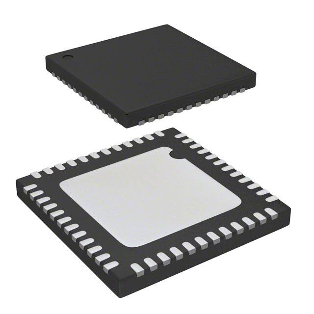


 工商网监
湘ICP备2023018690号
工商网监
湘ICP备2023018690号
