EFM32 Leopard Gecko Family
EFM32LG Data Sheet
The EFM32 Leopard Gecko MCUs are the world’s most energyfriendly microcontrollers.
The EFM32LG offers unmatched performance and ultra-low power consumption in both
active and sleep modes. EFM32LG devices consume as little as 0.65 μA in Stop mode
and 211 μA/MHz in Run mode. It also features autonomous peripherals, high overall chip
and analog integration, and the performance of the industry standard 32-bit ARM CortexM3 processor, making it perfect for battery-powered systems and systems with high-performance, low-energy requirements.
ARM Cortex
M3 processor
Clock Management
Memory
Protection Unit
Flash Program
Memory
Debug w/ ETM
RAM Memory
DMA Controller
• Ultra-low power operation
• 0.65 μA current in Stop (EM3), with
brown-out detection and RAM retention
• 63 μA/MHz in EM1
• 211 μA/MHz in Run mode (EM0)
• Hardware cryptography (AES)
• Alarm and security systems
• Industrial and home automation
Core / Memory
TM
• ARM Cortex-M3 at 48 MHz
• Fast wake-up time of 2 µs
EFM32LG applications include the following:
• Energy, gas, water and smart metering
• Health and fitness applications
• Smart accessories
KEY FEATURES
• Up to 256 kB of flash and 32 kB of RAM
Energy Management
High Frequency
Crystal Oscillator
High Frequency
RC Oscillator
Voltage
Regulator
Voltage
Comparator
Auxiliary High
Freq. RC Osc.
Low Freq.
RC Oscillator
Brown-out
Detector
Power-on
Reset
Low Frequency
Crystal Oscillator
Ultra Low Freq.
RC Oscillator
Back-up Power
Domain
Security
Hardware AES
32-bit bus
Peripheral Reflex System
Serial Interfaces
USART
Low Energy
UARTTM
UART
I2C
USB
I/O Ports
External Bus
Interface
Timers and Triggers
TFT Driver
External
Interrupts
General
Purpose I/O
Pin Reset
Pin Wakeup
Timer/Counter
LESENSE
Low Energy Timer
Real Time Counter
Pulse Counter
Watchdog Timer
Analog Interfaces
ADC
LCD Controller
DAC
Operational
Amplifier
Analog
Comparator
Back-up RTC
Lowest power mode with peripheral operational:
EM0 - Active
silabs.com | Building a more connected world.
EM1 - Sleep
EM2 – Deep Sleep
EM3 - Stop
Copyright © 2022 by Silicon Laboratories
EM4 - Shutoff
Rev. 2.40
�EFM32LG Data Sheet
Feature List
1. Feature List
• ARM Cortex-M3 CPU platform
• High Performance 32-bit processor @ up to 48 MHz
• Memory Protection Unit
• Wake-up Interrupt Controller
• SysTick System Timer
• Flexible Energy Management System
• 20 nA @ 3 V Shutoff Mode
• 0.4 µA @ 3 V Shutoff Mode with RTC
• 0.65 µA @ 3 V Stop Mode, including Power-on Reset, Brown-out Detector, RAM and CPU retention
• 0.95 µA @ 3 V Deep Sleep Mode, including RTC with 32.768 kHz oscillator, Power-on Reset, Brown-out Detector, RAM and
CPU retention
• 63 µA/MHz @ 3 V Sleep Mode
• 211 µA/MHz @ 3 V Run Mode, with code executed from flash
• 256/128/64 kB flash
• 32 kB RAM
• Up to 93 General Purpose I/O pins
• Configurable push-pull, open-drain, pull-up/down, input filter, drive strength
• Configurable peripheral I/O locations
• 16 asynchronous external interrupts
• Output state retention and wake-up from Shutoff Mode
• 12 Channel DMA Controller
• 12 Channel Peripheral Reflex System (PRS) for autonomous inter-peripheral signaling
• Hardware AES with 128/256-bit keys in 54/75 cycles
• Timers/Counters
• 4× 16-bit Timer/Counter
• 4×3 Compare/Capture/PWM channels
• Dead-Time Insertion on TIMER0
• 16-bit Low Energy Timer
• 1× 24-bit Real-Time Counter and 1× 32-bit Real-Time Counter
• 3× 16/8-bit Pulse Counter
• Watchdog Timer with dedicated RC oscillator @ 50 nA
• Integrated LCD Controller for up to 8×36 segments
• Voltage boost, adjustable contrast, and autonomous animation
• Backup Power Domain
• RTC and retention registers in a separate power domain, available in all energy modes
• Operation from backup battery when main power drains out
• External Bus Interface for up to 4x256 MB of external memory mapped space
• TFT Controller with Direct Drive
• Communication interfaces
• Up to 3× Universal Synchronous/Asynchronous Receiver/Transmitter
• UART/SPI/SmartCard (ISO 7816)/IrDA/I2S
• 2× Universal Asynchronous Receiver/Transmitter
• 2× Low Energy UART
• Autonomous operation with DMA in Deep Sleep Mode
• 2× I2C Interface with SMBus support
• Address recognition in Stop Mode
• Universal Serial Bus (USB) with Host & OTG support
• Fully USB 2.0 compliant
• On-chip PHY and embedded 5 to 3.3 V regulator
silabs.com | Building a more connected world.
Rev. 2.40 | 2
�EFM32LG Data Sheet
Feature List
• Ultra-low power precision analog peripherals
• 12-bit 1 Msamples/s Analog to Digital Converter
• 8 single-ended channels/4 differential channels
• On-chip temperature sensor
• 12-bit 500 ksamples/s Digital to Analog Converter
• 2 single-ended channels/1 differential channel
• Up to 2× Analog Comparator
• Capacitive sensing with up to 16 inputs
• 3× Operational Amplifier
• 6.1 MHz GBW, Rail-to-rail, Programmable Gain
• Supply Voltage Comparator
• Low Energy Sensor Interface (LESENSE)
• Autonomous sensor monitoring in Deep Sleep Mode
• Wide range of sensors supported, including LC sensors and capacitive buttons
• Ultra efficient Power-on Reset and Brown-Out Detector
• Debug Interface
• 2-pin Serial Wire Debug interface
• 1-pin Serial Wire Viewer
• Embedded Trace Module v3.5 (ETM)
• Pre-programmed USB/UART Bootloader
• Temperature range -40 to 85 ºC
• Single power supply 1.98 to 3.8 V
• Packages:
• BGA112
• BGA120
• CSP81
• LQFP100
• TQFP64
• QFN64
• Full wafer
silabs.com | Building a more connected world.
Rev. 2.40 | 3
�EFM32LG Data Sheet
Ordering Information
2. Ordering Information
The following table shows the available EFM32LG devices.
Table 2.1. Ordering Information
Flash (kB)
RAM (kB)
Max Speed
(MHz)
Supply
Voltage (V)
Temperature
(ºC)
Package
EFM32LG230F64G-F-QFN64
64
32
48
1.98 - 3.8
-40 - 85
QFN64
EFM32LG230F128G-F-QFN64
128
32
48
1.98 - 3.8
-40 - 85
QFN64
EFM32LG230F256G-F-QFN64
256
32
48
1.98 - 3.8
-40 - 85
QFN64
EFM32LG232F64G-F-QFP64
64
32
48
1.98 - 3.8
-40 - 85
TQFP64
EFM32LG232F128G-F-QFP64
128
32
48
1.98 - 3.8
-40 - 85
TQFP64
EFM32LG232F256G-F-QFP64
256
32
48
1.98 - 3.8
-40 - 85
TQFP64
EFM32LG280F64G-F-QFP1001
64
32
48
1.98 - 3.8
-40 - 85
LQFP100
EFM32LG280F128G-F-QFP100
128
32
48
1.98 - 3.8
-40 - 85
LQFP100
EFM32LG280F256G-F-QFP100
256
32
48
1.98 - 3.8
-40 - 85
LQFP100
EFM32LG290F64G-F-BGA1121
64
32
48
1.98 - 3.8
-40 - 85
BGA112
EFM32LG290F128G-F-BGA1121
128
32
48
1.98 - 3.8
-40 - 85
BGA112
EFM32LG290F256G-F-BGA112
256
32
48
1.98 - 3.8
-40 - 85
BGA112
EFM32LG295F64G-F-BGA1201
64
32
48
1.98 - 3.8
-40 - 85
BGA120
EFM32LG295F128G-F-BGA1201
128
32
48
1.98 - 3.8
-40 - 85
BGA120
EFM32LG295F256G-F-BGA120
256
32
48
1.98 - 3.8
-40 - 85
BGA120
EFM32LG330F64G-F-QFN641
64
32
48
1.98 - 3.8
-40 - 85
QFN64
EFM32LG330F128G-F-QFN64
128
32
48
1.98 - 3.8
-40 - 85
QFN64
EFM32LG330F256G-F-QFN64
256
32
48
1.98 - 3.8
-40 - 85
QFN64
EFM32LG332F64G-F-QFP641
64
32
48
1.98 - 3.8
-40 - 85
TQFP64
EFM32LG332F128G-F-QFP64
128
32
48
1.98 - 3.8
-40 - 85
TQFP64
EFM32LG332F256G-F-QFP64
256
32
48
1.98 - 3.8
-40 - 85
TQFP64
EFM32LG360F64G-F-CSP811
64
32
48
1.98 - 3.8
-40 - 85
CSP81
EFM32LG360F128G-F-CSP811
128
32
48
1.98 - 3.8
-40 - 85
CSP81
EFM32LG360F256G-F-CSP81
256
32
48
1.98 - 3.8
-40 - 85
CSP81
EFM32LG380F64G-F-QFP1001
64
32
48
1.98 - 3.8
-40 - 85
LQFP100
EFM32LG380F128G-F-QFP1001
128
32
48
1.98 - 3.8
-40 - 85
LQFP100
EFM32LG380F256G-F-QFP100
256
32
48
1.98 - 3.8
-40 - 85
LQFP100
EFM32LG390F64G-F-BGA1121
64
32
48
1.98 - 3.8
-40 - 85
BGA112
EFM32LG390F128G-F-BGA1121
128
32
48
1.98 - 3.8
-40 - 85
BGA112
EFM32LG390F256G-F-BGA112
256
32
48
1.98 - 3.8
-40 - 85
BGA112
EFM32LG395F64G-F-BGA1201
64
32
48
1.98 - 3.8
-40 - 85
BGA120
Ordering Code
silabs.com | Building a more connected world.
Rev. 2.40 | 4
�EFM32LG Data Sheet
Ordering Information
Flash (kB)
RAM (kB)
Max Speed
(MHz)
Supply
Voltage (V)
Temperature
(ºC)
Package
EFM32LG395F128G-F-BGA1201
128
32
48
1.98 - 3.8
-40 - 85
BGA120
EFM32LG395F256G-F-BGA120
256
32
48
1.98 - 3.8
-40 - 85
BGA120
EFM32LG840F64G-F-QFN64
64
32
48
1.98 - 3.8
-40 - 85
QFN64
EFM32LG840F128G-F-QFN64
128
32
48
1.98 - 3.8
-40 - 85
QFN64
EFM32LG840F256G-F-QFN64
256
32
48
1.98 - 3.8
-40 - 85
QFN64
EFM32LG842F64G-F-QFP641
64
32
48
1.98 - 3.8
-40 - 85
TQFP64
EFM32LG842F128G-F-QFP64
128
32
48
1.98 - 3.8
-40 - 85
TQFP64
EFM32LG842F256G-F-QFP64
256
32
48
1.98 - 3.8
-40 - 85
TQFP64
EFM32LG880F64G-F-QFP100
64
32
48
1.98 - 3.8
-40 - 85
LQFP100
EFM32LG880F128G-F-QFP100
128
32
48
1.98 - 3.8
-40 - 85
LQFP100
EFM32LG880F256G-F-QFP100
256
32
48
1.98 - 3.8
-40 - 85
LQFP100
EFM32LG890F64G-F-BGA1121
64
32
48
1.98 - 3.8
-40 - 85
BGA112
EFM32LG890F128G-F-BGA1121
128
32
48
1.98 - 3.8
-40 - 85
BGA112
EFM32LG890F256G-F-BGA112
256
32
48
1.98 - 3.8
-40 - 85
BGA112
EFM32LG895F64G-F-BGA1201
64
32
48
1.98 - 3.8
-40 - 85
BGA120
EFM32LG895F128G-F-BGA1201
128
32
48
1.98 - 3.8
-40 - 85
BGA120
EFM32LG895F256G-F-BGA120
256
32
48
1.98 - 3.8
-40 - 85
BGA120
EFM32LG900F256G-F-D1I 1
256
32
48
1.98 - 3.8
-40 - 85
Wafer
EFM32LG940F64G-F-QFN641
64
32
48
1.98 - 3.8
-40 - 85
QFN64
EFM32LG940F128G-F-QFN64
128
32
48
1.98 - 3.8
-40 - 85
QFN64
EFM32LG940F256G-F-QFN64
256
32
48
1.98 - 3.8
-40 - 85
QFN64
EFM32LG942F64G-F-QFP641
64
32
48
1.98 - 3.8
-40 - 85
TQFP64
EFM32LG942F128G-F-QFP64
128
32
48
1.98 - 3.8
-40 - 85
TQFP64
EFM32LG942F256G-F-QFP64
256
32
48
1.98 - 3.8
-40 - 85
TQFP64
EFM32LG980F64G-F-QFP1001
64
32
48
1.98 - 3.8
-40 - 85
LQFP100
EFM32LG980F128G-F-QFP1001
128
32
48
1.98 - 3.8
-40 - 85
LQFP100
EFM32LG980F256G-F-QFP100
256
32
48
1.98 - 3.8
-40 - 85
LQFP100
EFM32LG990F64G-F-BGA1121
64
32
48
1.98 - 3.8
-40 - 85
BGA112
EFM32LG990F128G-F-BGA1121
128
32
48
1.98 - 3.8
-40 - 85
BGA112
EFM32LG990F256G-F-BGA112
256
32
48
1.98 - 3.8
-40 - 85
BGA112
EFM32LG995F64G-F-BGA1201
64
32
48
1.98 - 3.8
-40 - 85
BGA120
EFM32LG995F128G-F-BGA1201
128
32
48
1.98 - 3.8
-40 - 85
BGA120
EFM32LG995F256G-F-BGA120
256
32
48
1.98 - 3.8
-40 - 85
BGA120
Ordering Code
Note:
1. Not recommended for new designs.
silabs.com | Building a more connected world.
Rev. 2.40 | 5
�EFM32LG Data Sheet
Ordering Information
EFM32 LG 995 F 256 G – F – BGA 120 R
Tape and Reel (Optional)
Pin Count
Package
Revision
Temperature Grade – G (-40 to +85 °C)
Memory Size in kB
Memory Type (Flash)
Feature Set Code
Leopard Gecko
Energy Friendly Microcontroller 32-bit
Figure 2.1. Ordering Code Decoder
Adding the suffix 'R' to the part number (e.g. EFM32LGF256G-F-BGA120R) denotes tape and reel.
Visit www.silabs.com for information on global distributors and representatives.
silabs.com | Building a more connected world.
Rev. 2.40 | 6
�Table of Contents
1. Feature List . . . . . . . . . . . . . . . . . . . . . . . . . . . . . . . . 2
2. Ordering Information . . . . . . . . . . . . . . . . . . . . . . . . . . . . 4
3. System Summary . . . . . . . . . . . . . . . . . . . . . . . . . . . . .
13
3.1 System Introduction . . . . . . . . . . . . . . . . . . .
3.1.1 ARM Cortex-M3 Core . . . . . . . . . . . . . . . . .
3.1.2 Debug Interface (DBG) . . . . . . . . . . . . . . . . .
3.1.3 Memory System Controller (MSC) . . . . . . . . . . . . .
3.1.4 Direct Memory Access Controller (DMA) . . . . . . . . . . .
3.1.5 Reset Management Unit (RMU) . . . . . . . . . . . . . .
3.1.6 Energy Management Unit (EMU) . . . . . . . . . . . . .
3.1.7 Clock Management Unit (CMU) . . . . . . . . . . . . . .
3.1.8 Watchdog (WDOG) . . . . . . . . . . . . . . . . . .
3.1.9 Peripheral Reflex System (PRS) . . . . . . . . . . . . .
3.1.10 External Bus Interface (EBI) . . . . . . . . . . . . . .
3.1.11 TFT Direct Drive . . . . . . . . . . . . . . . . . .
3.1.12 Universal Serial Bus Controller (USB) . . . . . . . . . . .
3.1.13 Inter-Integrated Circuit Interface (I2C) . . . . . . . . . . .
3.1.14 Universal Synchronous/Asynchronous Receiver/Transmitter (USART)
3.1.15 Pre-Programmed USB/UART Bootloader . . . . . . . . . .
3.1.16 Universal Asynchronous Receiver/Transmitter (UART) . . . . .
3.1.17 Low Energy Universal Asynchronous Receiver/Transmitter (LEUART)
3.1.18 Timer/Counter (TIMER) . . . . . . . . . . . . . . . .
3.1.19 Real Time Counter (RTC) . . . . . . . . . . . . . . .
3.1.20 Backup Real Time Counter (BURTC) . . . . . . . . . . .
3.1.21 Low Energy Timer (LETIMER) . . . . . . . . . . . . . .
3.1.22 Pulse Counter (PCNT) . . . . . . . . . . . . . . . .
3.1.23 Analog Comparator (ACMP) . . . . . . . . . . . . . .
3.1.24 Voltage Comparator (VCMP) . . . . . . . . . . . . . .
3.1.25 Analog to Digital Converter (ADC) . . . . . . . . . . . .
3.1.26 Digital to Analog Converter (DAC) . . . . . . . . . . . .
3.1.27 Operational Amplifier (OPAMP) . . . . . . . . . . . . .
3.1.28 Low Energy Sensor Interface (LESENSE) . . . . . . . . . .
3.1.29 Backup Power Domain . . . . . . . . . . . . . . . .
3.1.30 Advanced Encryption Standard Accelerator (AES) . . . . . . .
3.1.31 General Purpose Input/Output (GPIO) . . . . . . . . . . .
3.1.32 Liquid Crystal Display Driver (LCD) . . . . . . . . . . . .
.
.
.
.
.
.
.
.
.
.
.
.
.
.
.
.
.
.
.
.
.
.
.
.
.
.
.
.
.
.
.
.
.
.
.
.
.
.
.
.
.
.
.
.
.
.
.
.
.
.
.
.
.
.
.
.
.
.
.
.
.
.
.
.
.
.
.
.
.
.
.
.
.
.
.
.
.
.
.
.
.
.
.
.
.
.
.
.
.
.
.
.
.
.
.
.
.
.
.
.
.
.
.
.
.
.
.
.
.
.
.
.
.
.
.
.
.
.
.
.
.
.
.
.
.
.
.
.
.
.
.
.
.
.
.
.
.
.
.
.
.
.
.
.
.
.
.
.
.
.
.
.
.
.
.
.
.
.
.
.
.
.
.
.
.
.
.
.
.
.
.
.
.
.
.
.
.
.
.
.
.
.
.
.
.
.
.
.
.
.
.
.
.
.
.
.
.
.
.
.
.
.
.
.
.
.
.
.
.
.
.
.
.
.
.
.
.
.
.
.
.
.
.
.
.
.
.
.
.
.
.
.
.
.
.
.
.
.
.
.
.
.
.
.
.
.
.
.
.
.
.
.
.
.
.
.
.
.
.
.
.
.
.
.
.13
.13
.13
.13
.13
.13
.14
.14
.14
.14
.14
.14
.14
.14
.14
.15
.15
.15
.15
.15
.15
.15
.15
.15
.15
.16
.16
.16
.16
.16
.16
.16
.16
3.2 Configuration Summary
3.2.1 EFM32LG230 . .
3.2.2 EFM32LG232 . .
3.2.3 EFM32LG280 . .
3.2.4 EFM32LG290 . .
3.2.5 EFM32LG295 . .
3.2.6 EFM32LG330 . .
3.2.7 EFM32LG332 . .
.
.
.
.
.
.
.
.
.
.
.
.
.
.
.
.
.
.
.
.
.
.
.
.
.
.
.
.
.
.
.
.
.
.
.
.
.
.
.
.
.
.
.
.
.
.
.
.
.
.
.
.
.
.
.
.
.
.
.
.
.
.
.
.
.16
.17
.19
.21
.23
.25
.27
.29
.
.
.
.
.
.
.
.
silabs.com | Building a more connected world.
.
.
.
.
.
.
.
.
.
.
.
.
.
.
.
.
.
.
.
.
.
.
.
.
.
.
.
.
.
.
.
.
.
.
.
.
.
.
.
.
.
.
.
.
.
.
.
.
.
.
.
.
.
.
.
.
.
.
.
.
.
.
.
.
.
.
.
.
.
.
.
.
.
.
.
.
.
.
.
.
.
.
.
.
.
.
.
.
.
.
.
.
.
.
.
.
.
.
.
.
.
.
.
.
.
.
.
.
.
.
.
.
.
.
.
.
.
.
.
.
.
.
.
.
.
.
.
.
.
.
.
.
.
.
.
.
Rev. 2.40 | 7
�3.2.8 EFM32LG360 .
3.2.9 EFM32LG380 .
3.2.10 EFM32LG390
3.2.11 EFM32LG395
3.2.12 EFM32LG840
3.2.13 EFM32LG842
3.2.14 EFM32LG880
3.2.15 EFM32LG890
3.2.16 EFM32LG895
3.2.17 EFM32LG900
3.2.18 EFM32LG940
3.2.19 EFM32LG942
3.2.20 EFM32LG980
3.2.21 EFM32LG990
3.2.22 EFM32LG995
3.3 Memory Map
.
.
.
.
.
.
.
.
.
.
.
.
.
.
.
.
.
.
.
.
.
.
.
.
.
.
.
.
.
.
.
.
.
.
.
.
.
.
.
.
.
.
.
.
.
.
.
.
.
.
.
.
.
.
.
.
.
.
.
.
.
.
.
.
.
.
.
.
.
.
.
.
.
.
.
.
.
.
.
.
.
.
.
.
.
.
.
.
.
.
.
.
.
.
.
.
.
.
.
.
.
.
.
.
.
.
.
.
.
.
.
.
.
.
.
.
.
.
.
.
.
.
.
.
.
.
.
.
.
.
.
.
.
.
.
.
.
.
.
.
.
.
.
.
.
.
.
.
.
.
.
.
.
.
.
.
.
.
.
.
.
.
.
.
.
.
.
.
.
.
.
.
.
.
.
.
.
.
.
.
.
.
.
.
.
.
.
.
.
.
.
.
.
.
.
.
.
.
.
.
.
.
.
.
.
.
.
.
.
.
.
.
.
.
.
.
.
.
.
.
.
.
.
.
.
.
.
.
.
.
.
.
.
.
.
.
.
.
.
.
.
.
.
.
.
.
.
.
.
.
.
.
.
.
.
.
.
.
.
.
.
.
.
.
.
.
.
.
.
.
.
.
.
.
.
.
.
.
.
.
.
.
.
.
.
.
.
.
.
.
.
.
.
.
.
.
.
.
.
.
.
.
.
.
.
.
.
.
.
.
.
.
.
.
.
.
.
.
.
.
.
.
.
.
.
.
.
.
.
.
.
.
.
.
.
.
.
.
.
.
.
.
.
.
.
.
.
.
.
.
.
.
.
.
.
.
.
.
.
.
.
.
.
.
.
.
.
.
.
.
.
.
.
.
.
.
.
.
.
.
.
.
.
.
.
.
.
.
.
.
.
.
.
.
.
.
.
.
.
.
.
.
.
.
.
.
.
.31
.33
.35
.37
.39
.41
.43
.45
.47
.49
.51
.53
.55
.57
.59
.
.
.
.
.
.
.
.
.
.
.
.
.
.
.
.
.
.
.
.
.
.
.
.
.
.
.
.61
4. Electrical Characteristics . . . . . . . . . . . . . . . . . . . . . . . . . . 63
4.1 Test Conditions . . . . . . . .
4.1.1 Typical Values . . . . . .
4.1.2 Minimum and Maximum Values .
.
.
.
.
.
.
.
.
.
.
.
.
.
.
.
.
.
.
.
.
.
.
.
.
.
.
.
.
.
.
.
.
.
.
.
.
.
.
.
.
.
.
.
.
.
.
.
.
.
.
.
.
.
.
.
.
.
.
.
.
.
.
.
.63
.63
.63
4.2 Absolute Maximum Ratings.
.
.
.
.
.
.
.
.
.
.
.
.
.
.
.
.
.
.
.
.
.
.
.
.
.63
4.3 General Operating Conditions .
.
.
.
.
.
.
.
.
.
.
.
.
.
.
.
.
.
.
.
.
.
.
.
.63
4.4 Backup Supply Domain .
.
.
.
.
.
.
.
.
.
.
.
.
.
.
.
.
.
.
.
.
.
.
.
.
.64
4.5 Current Consumption . . . .
4.5.1 EM1 Current Consumption
4.5.2 EM2 Current Consumption
4.5.3 EM3 Current Consumption
4.5.4 EM4 Current Consumption
.
.
.
.
.
.
.
.
.
.
.
.
.
.
.
.
.
.
.
.
.
.
.
.
.
.
.
.
.
.
.
.
.
.
.
.
.
.
.
.
.
.
.
.
.
.
.
.
.
.
.
.
.
.
.
.
.
.
.
.
.
.
.
.
.
.
.
.
.
.
.
.
.
.
.
.
.
.
.
.
.
.
.
.
.
.
.
.
.
.
.
.
.
.
.
.
.
.
.
.
.
.
.
.
.
.
.
.
.
.
.
.
.
.
.
.65
.67
.70
.71
.71
4.6 Transition between Energy Modes .
.
.
.
.
.
.
.
.
.
.
.
.
.
.
.
.
.
.
.
.
.
.72
4.7 Power Management .
.
.
.
.
.
.
.
.
.
.
.
.
.
.
.
.
.
.
.
.
.
.
.
.
.
.
.72
4.8 Flash .
.
.
.
.
.
.
.
.
.
.
.
.
.
.
.
.
.
.
.
.
.
.
.
.
.
.
.73
4.9 General Purpose Input Output .
.
.
.
.
.
.
.
.
.
.
.
.
.
.
.
.
.
.
.
.
.
.
.
.74
4.10 Oscillators . .
4.10.1 LFXO . .
4.10.2 HFXO . .
4.10.3 LFRCO .
4.10.4 HFRCO .
4.10.5 AUXHFRCO
4.10.6 ULFRCO .
.
.
.
.
.
.
.
.
.
.
.
.
.
.
.
.
.
.
.
.
.
.
.
.
.
.
.
.
.
.
.
.
.
.
.
.
.
.
.
.
.
.
.
.
.
.
.
.
.
.
.
.
.
.
.
.
.
.
.
.
.
.
.
.
.
.
.
.
.
.
.
.
.
.
.
.
.
.
.
.
.
.
.
.
.
.
.
.
.
.
.
.
.
.
.
.
.
.
.
.
.
.
.
.
.
.
.
.
.
.
.
.
.
.
.
.
.
.
.
.
.
.
.
.
.
.
.
.
.
.
.
.
.
.
.
.
.
.
.
.
.
.
.
.
.
.
.
.
.
.
.
.
.
.
.
.
.
.
.
.
.
.82
.82
.83
.84
.85
.90
.90
4.11 Analog Digital Converter (ADC) .
4.11.1 Typical Performance . . .
.
.
.
.
.
.
.
.
.
.
.
.
.
.
.
.
.
.
.
.
.
.
.
.
.
.
.
.
.
.
.
.
.
.
.
.
.
.
.
.
.
.
.
.
.91
.97
.
.
.
.
.
.
.
.
.
.
.
.
.
.
.
.
.
.
.
.
.
.
.
.
.
.
.
.
.
.
.
.
.
.
.
.
.
.
.
.
.
4.12 Digital Analog Converter (DAC) .
.
.
.
.
.
.
.
.
.
.
.
.
.
.
.
.
.
.
.
.
.
. 102
4.13 Operational Amplifier (OPAMP) .
.
.
.
.
.
.
.
.
.
.
.
.
.
.
.
.
.
.
.
.
.
. 104
silabs.com | Building a more connected world.
Rev. 2.40 | 8
�4.14 Analog Comparator (ACMP) .
.
4.15 Voltage Comparator (VCMP) .
4.16 EBI
4.17 LCD
4.18 I2C
.
.
.
.
.
.
.
.
4.19 USART SPI
.
.
.
.
.
.
.
.
.
.
.
.
.
.
.
.
.
.
.
.
.
.
.
.
.
.
.
.
.
.
.
.
.
.
.
.
.
.
.
.
.
.
.
.
.
.
.
.
.
.
.
.
.
.
.
.
.
.
.
.
.
.
.
.
.
.
.
.
.
.
.
.
.
.
.
.
.
.
.
.
.
.
.
.
.
.
.
.
.
.
.
.
.
.
.
.
. 111
. 119
.
.
.
.
1
. 20
. 125
.
.
.
.
.
.
.
.
.
.
.
.
.
.
.
.
.
.
.
.
.
.
.
.
.
.
.
. 1. 26
.
.
.
.
.
.
.
.
.
.
.
.
.
.
.
.
.
.
.
.
.
.
.
.
.
.
.
. 128
.
.
.
.
.
.
.
.
.
.
.
.
.
.
.
.
.
.
.
.
.
.
.
.
.
.
.
4.20 Digital Peripherals
.130
5. Pin Definitions . . . . . . . . . . . . . . . . . . . . . . . . . . . . . . 131
5.1 EFM32LG230 (QFN64) . . . . . . . . . . . . . . . . . . . . . . . . . . 131
5.1.1 Pinout
. . . . . . . . . . . . . . . . . . . . . . . . . . . . . 1
. 31
5.1.2 Alternate Functionality Pinout
. . . . . . . . . . . . . . . . . . . . . 135
.
5.1.3 GPIO Pinout Overview . . . . . . . . . . . . . . . . . . . . . . . . . 140
5.1.4 Opamp Pinout Overview
. . . . . . . . . . . . . . . . . . . . . . . .140
5.2 EFM32LG232 (TQFP64)
. . . . . . . . . . . . . . . . . . . . . . . . 141
.
5.2.1 Pinout
. . . . . . . . . . . . . . . . . . . . . . . . . . . . . 1
. 41
5.2.2 Alternate Functionality Pinout
. . . . . . . . . . . . . . . . . . . . . 145
.
5.2.3 GPIO Pinout Overview . . . . . . . . . . . . . . . . . . . . . . . . . 149
5.2.4 Opamp Pinout Overview
. . . . . . . . . . . . . . . . . . . . . . . .150
5.3 EFM32LG280 (LQFP100)
. . . . . . . . . . . . . . . . . . . . . . . . .151
5.3.1 Pinout
. . . . . . . . . . . . . . . . . . . . . . . . . . . . . 1
. 51
5.3.2 Alternate Functionality Pinout
. . . . . . . . . . . . . . . . . . . . . 157
.
5.3.3 GPIO Pinout Overview . . . . . . . . . . . . . . . . . . . . . . . . . 164
5.3.4 Opamp Pinout Overview
. . . . . . . . . . . . . . . . . . . . . . . .164
5.4 EFM32LG290 (BGA112)
. . . . . . . . . . . . . . . . . . . . . . . . 165
.
5.4.1 Pinout
. . . . . . . . . . . . . . . . . . . . . . . . . . . . . 1
. 65
5.4.2 Alternate Functionality Pinout
. . . . . . . . . . . . . . . . . . . . . 171
.
5.4.3 GPIO Pinout Overview . . . . . . . . . . . . . . . . . . . . . . . . . 178
5.4.4 Opamp Pinout Overview
. . . . . . . . . . . . . . . . . . . . . . . .178
5.5 EFM32LG295 (BGA120)
. . . . . . . . . . . . . . . . . . . . . . . . 179
.
5.5.1 Pinout
. . . . . . . . . . . . . . . . . . . . . . . . . . . . . 1
. 79
5.5.2 Alternate Functionality Pinout
. . . . . . . . . . . . . . . . . . . . . 185
.
5.5.3 GPIO Pinout Overview . . . . . . . . . . . . . . . . . . . . . . . . . 192
5.5.4 Opamp Pinout Overview
. . . . . . . . . . . . . . . . . . . . . . . .192
5.6 EFM32LG330 (QFN64) . . . . . . . . . . . . . . . . . . . . . . . . . . 193
5.6.1 Pinout
. . . . . . . . . . . . . . . . . . . . . . . . . . . . . 1
. 93
5.6.2 Alternate Functionality Pinout
. . . . . . . . . . . . . . . . . . . . . 197
.
5.6.3 GPIO Pinout Overview . . . . . . . . . . . . . . . . . . . . . . . . . 202
5.6.4 Opamp Pinout Overview
. . . . . . . . . . . . . . . . . . . . . . . .202
5.7 EFM32LG332 (TQFP64)
. . . . . . . . . . . . . . . . . . . . . . . . 203
.
5.7.1 Pinout
. . . . . . . . . . . . . . . . . . . . . . . . . . . . . 2
. 03
5.7.2 Alternate Functionality Pinout
. . . . . . . . . . . . . . . . . . . . . 207
.
5.7.3 GPIO Pinout Overview . . . . . . . . . . . . . . . . . . . . . . . . . 211
5.7.4 Opamp Pinout Overview
. . . . . . . . . . . . . . . . . . . . . . . .212
5.8 EFM32LG360 (CSP81)
.
silabs.com | Building a more connected world.
.
.
.
.
.
.
.
.
.
.
.
.
.
.
.
.
.
.
.
.
.
.
.
.
. 213
Rev. 2.40 | 9
�5.8.1
5.8.2
5.8.3
5.8.4
Pinout
. . . . . . . . . . . . . . . . . . . . . . . . . . . . . 2
. 13
Alternate Functionality Pinout
. . . . . . . . . . . . . . . . . . . . . 218
.
GPIO Pinout Overview . . . . . . . . . . . . . . . . . . . . . . . . . 223
Opamp Pinout Overview
. . . . . . . . . . . . . . . . . . . . . . . .223
5.9 EFM32LG380 (LQFP100)
. . . . . . . . . . . . . . . . . . . . . . . . .224
5.9.1 Pinout
. . . . . . . . . . . . . . . . . . . . . . . . . . . . . 2
. 24
5.9.2 Alternate Functionality Pinout
. . . . . . . . . . . . . . . . . . . . . 229
.
5.9.3 GPIO Pinout Overview . . . . . . . . . . . . . . . . . . . . . . . . . 236
5.9.4 Opamp Pinout Overview
. . . . . . . . . . . . . . . . . . . . . . . .236
5.10 EFM32LG390 (BGA112) . . . . . . . . . . . . . . . . . . . . . . . . .237
5.10.1 Pinout . . . . . . . . . . . . . . . . . . . . . . . . . . . . . . 237
5.10.2 Alternate Functionality Pinout . . . . . . . . . . . . . . . . . . . . . .243
5.10.3 GPIO Pinout Overview
. . . . . . . . . . . . . . . . . . . . . . . 2
. 50
5.10.4 Opamp Pinout Overview . . . . . . . . . . . . . . . . . . . . . . . . 250
5.11 EFM32LG395 (BGA120) . . . . . . . . . . . . . . . . . . . . . . . . .251
5.11.1 Pinout . . . . . . . . . . . . . . . . . . . . . . . . . . . . . . 251
5.11.2 Alternate Functionality Pinout . . . . . . . . . . . . . . . . . . . . . .257
5.11.3 GPIO Pinout Overview
. . . . . . . . . . . . . . . . . . . . . . . 2
. 64
5.11.4 Opamp Pinout Overview . . . . . . . . . . . . . . . . . . . . . . . . 265
5.12 EFM32LG840 (QFN64)
. . . . . . . . . . . . . . . . . . . . . . . . 266
.
5.12.1 Pinout . . . . . . . . . . . . . . . . . . . . . . . . . . . . . . 266
5.12.2 Alternate Functionality Pinout . . . . . . . . . . . . . . . . . . . . . .270
5.12.3 GPIO Pinout Overview
. . . . . . . . . . . . . . . . . . . . . . . 2
. 76
5.12.4 Opamp Pinout Overview . . . . . . . . . . . . . . . . . . . . . . . . 276
5.13 EFM32LG842 (TQFP64) . . . . . . . . . . . . . . . . . . . . . . . . .277
5.13.1 Pinout . . . . . . . . . . . . . . . . . . . . . . . . . . . . . . 277
5.13.2 Alternate Functionality Pinout . . . . . . . . . . . . . . . . . . . . . .281
5.13.3 GPIO Pinout Overview
. . . . . . . . . . . . . . . . . . . . . . . 2
. 87
5.13.4 Opamp Pinout Overview . . . . . . . . . . . . . . . . . . . . . . . . 287
5.14 EFM32LG880 (LQFP100) . . . . . . . . . . . . . . . . . . . . . . . . . 288
5.14.1 Pinout . . . . . . . . . . . . . . . . . . . . . . . . . . . . . . 288
5.14.2 Alternate Functionality Pinout . . . . . . . . . . . . . . . . . . . . . .294
5.14.3 GPIO Pinout Overview
. . . . . . . . . . . . . . . . . . . . . . . 3
. 03
5.14.4 Opamp Pinout Overview . . . . . . . . . . . . . . . . . . . . . . . . 304
5.15 EFM32LG890 (BGA112) . . . . . . . . . . . . . . . . . . . . . . . . .305
5.15.1 Pinout . . . . . . . . . . . . . . . . . . . . . . . . . . . . . . 305
5.15.2 Alternate Functionality Pinout . . . . . . . . . . . . . . . . . . . . . .311
5.15.3 GPIO Pinout Overview
. . . . . . . . . . . . . . . . . . . . . . . 3
. 20
5.15.4 Opamp Pinout Overview . . . . . . . . . . . . . . . . . . . . . . . . 321
5.16 EFM32LG895 (BGA120) . . . . . . . . . . . . . . . . . . . . . . . . .322
5.16.1 Pinout . . . . . . . . . . . . . . . . . . . . . . . . . . . . . . 322
5.16.2 Alternate Functionality Pinout . . . . . . . . . . . . . . . . . . . . . .328
5.16.3 GPIO Pinout Overview
. . . . . . . . . . . . . . . . . . . . . . . 3
. 37
5.16.4 Opamp Pinout Overview . . . . . . . . . . . . . . . . . . . . . . . . 337
5.17 EFM32LG900 (Wafer) . . . . . . . . . . . . . . . . . . . . . . . . . . 338
5.17.1 Padout . . . . . . . . . . . . . . . . . . . . . . . . . . . . . . 338
silabs.com | Building a more connected world.
Rev. 2.40 | 10
�5.17.2 Alternate Functionality Padout . . . . . . . . . . . . . . . . . . . . . . 344
5.17.3 GPIO Pinout Overview
. . . . . . . . . . . . . . . . . . . . . . . 3
. 53
5.17.4 Opamp Pinout Overview . . . . . . . . . . . . . . . . . . . . . . . . 354
5.18 EFM32LG940 (QFN64)
. . . . . . . . . . . . . . . . . . . . . . . . 355
.
5.18.1 Pinout . . . . . . . . . . . . . . . . . . . . . . . . . . . . . . 355
5.18.2 Alternate Functionality Pinout . . . . . . . . . . . . . . . . . . . . . .359
5.18.3 GPIO Pinout Overview
. . . . . . . . . . . . . . . . . . . . . . . 3
. 65
5.18.4 Opamp Pinout Overview . . . . . . . . . . . . . . . . . . . . . . . . 365
5.19 EFM32LG942 (TQFP64) . . . . . . . . . . . . . . . . . . . . . . . . .366
5.19.1 Pinout . . . . . . . . . . . . . . . . . . . . . . . . . . . . . . 366
5.19.2 Alternate Functionality Pinout . . . . . . . . . . . . . . . . . . . . . .370
5.19.3 GPIO Pinout Overview
. . . . . . . . . . . . . . . . . . . . . . . 3
. 75
5.19.4 Opamp Pinout Overview . . . . . . . . . . . . . . . . . . . . . . . . 376
5.20 EFM32LG980 (LQFP100) . . . . . . . . . . . . . . . . . . . . . . . . . 377
5.20.1 Pinout . . . . . . . . . . . . . . . . . . . . . . . . . . . . . . 377
5.20.2 Alternate Functionality Pinout . . . . . . . . . . . . . . . . . . . . . .383
5.20.3 GPIO Pinout Overview
. . . . . . . . . . . . . . . . . . . . . . . 3
. 92
5.20.4 Opamp Pinout Overview . . . . . . . . . . . . . . . . . . . . . . . . 392
5.21 EFM32LG990 (BGA112) . . . . . . . . . . . . . . . . . . . . . . . . .393
5.21.1 Pinout . . . . . . . . . . . . . . . . . . . . . . . . . . . . . . 393
5.21.2 Alternate Functionality Pinout . . . . . . . . . . . . . . . . . . . . . .399
5.21.3 GPIO Pinout Overview
. . . . . . . . . . . . . . . . . . . . . . . 4
. 08
5.21.4 Opamp Pinout Overview . . . . . . . . . . . . . . . . . . . . . . . . 408
5.22 EFM32LG995 (BGA120) . . . . . . . . . . . . . . . . . . . . . . . . .409
5.22.1 Pinout . . . . . . . . . . . . . . . . . . . . . . . . . . . . . . 409
5.22.2 Alternate Functionality Pinout . . . . . . . . . . . . . . . . . . . . . .415
5.22.3 GPIO Pinout Overview
. . . . . . . . . . . . . . . . . . . . . . . 4
. 24
5.22.4 Opamp Pinout Overview . . . . . . . . . . . . . . . . . . . . . . . . 425
6. BGA112 Package Specifications
. . . . . . . . . . . . . . . . . . . . . . .426
6.1 BGA112 Package Dimensions .
.
.
.
.
.
.
.
.
.
.
.
.
.
.
.
.
.
.
.
.
.
.
. 426
6.2 BGA112 PCB Layout .
.
.
.
.
.
.
.
.
.
.
.
.
.
.
.
.
.
.
.
.
.
.
.
.
.
. 427
6.3 BGA112 Package Marking .
.
.
.
.
.
.
.
.
.
.
.
.
.
.
.
.
.
.
.
.
.
.
.
. 429
7. BGA120 Package Specifications
. . . . . . . . . . . . . . . . . . . . . . .430
7.1 BGA120 Package Dimensions .
.
.
.
.
.
.
.
.
.
.
.
.
.
.
.
.
.
.
.
.
.
.
. 430
7.2 BGA120 PCB Layout .
.
.
.
.
.
.
.
.
.
.
.
.
.
.
.
.
.
.
.
.
.
.
.
.
.
. 431
7.3 BGA120 Package Marking .
.
.
.
.
.
.
.
.
.
.
.
.
.
.
.
.
.
.
.
.
.
.
.
. 433
8. CSP81 Package Specifications . . . . . . . . . . . . . . . . . . . . . . . . 434
8.1 CSP81 Package Dimensions
8.2 CSP81 PCB Layout
.
.
8.3 CSP81 Package Marking
8.4 CSP81 Environmental
.
.
.
.
.
.
.
.
.
.
.
.
.
.
.
.
.
.
.
.
.
.
.
.
.434
.
.
.
.
.
.
.
.
.
.
.
.
.
.
.
.
.
.
.
.
.
.
.
.
.436
.
.
.
.
.
.
.
.
.
.
.
.
.
.
.
.
.
.
.
.
.
.
.
. 4
. 39
.
.
.
.
.
.
.
.
.
.
.
.
.
.
.
.
.
.
.
.
.
.
.
. 4. 39
9. LQFP100 Package Specifications . . . . . . . . . . . . . . . . . . . . . . . 440
silabs.com | Building a more connected world.
Rev. 2.40 | 11
�9.1 LQFP100 Package Dimensions
9.2 LQFP100 PCB Layout
.
.
.
.
.
.
.
.
.
.
.
.
.
.
.
.
.
.
.
.
.
.
.
.
.
.
.
.
.
.
.
.
.
.
.
.
.
.
.
.
.
.
.
.
.
.
. 4
. 42
.
.
.
.
.
.
.
.
.
.
.
.
.
.
.
.
.
.
.
.
.
.
. 444
.
9.3 LQFP100 Package Marking
10. QFN64 Package Specifications
.440
. . . . . . . . . . . . . . . . . . . . . . .445
10.1 QFN64 Package Dimensions.
.
.
.
.
.
.
.
.
.
.
.
.
.
.
.
.
.
.
.
.
.
.
. 445
10.2 QFN64 PCB Layout .
.
.
.
.
.
.
.
.
.
.
.
.
.
.
.
.
.
.
.
.
.
.
.
.
.
. 447
10.3 QFN64 Package Marking .
.
.
.
.
.
.
.
.
.
.
.
.
.
.
.
.
.
.
.
.
.
.
.
. 449
11. TQFP64 Package Specifications . . . . . . . . . . . . . . . . . . . . . . . 450
11.1 TQFP64 Package Dimensions
11.2 TQFP64 PCB Layout
.
.
.
.
.
.
.
.
.
.
.
.
.
.
.
.
.
.
.
.
.
.
.
.
.450
.
.
.
.
.
.
.
.
.
.
.
.
.
.
.
.
.
.
.
.
.
.
.
.452
.
.
.
.
.
.
.
.
.
.
.
.
.
.
.
.
.
.
.
.
.
.
. 4. 54
11.3 TQFP64 Package Marking
12. Wafer Specifications
. . . . . . . . . . . . . . . . . . . . . . . . . . .455
12.1 Bonding Instructions
.
12.2 Wafer Description
12.2.1 Environmental
.
.
.
.
.
.
.
.
.
.
12.4 Failure Analysis (FA) Guidelines
.
.
.
13.2 Soldering Information
.
.
.
.
.
.
.
.
.
.
.
.
.
.
.
.
.
. 455
.
.
.
.
.
.
.
.
.
.
.
.
.
.
.
.
.
.
.
.
.
. 456
.
.
.
.
.
.
.
.
.
.
.
.
.
.
.
.
.
.
.
.
. 456
.
13. Chip Revision, Solder Information, Errata
13.3 Errata
.
. . . . . . . . . . . . . . . . . . . . . . . . . . 4
. 55
. . . . . . . . . . . . . . . . . . . . . . . . . . .455
12.3 Wafer Storage Guidelines .
13.1 Chip Revision .
.
.
.
.
.
.
.
.
.
.
.
.
.
.
.
.
.
.
.
.
. . . . . . . . . . . . . . . . . . .457
.
.
.
.
.
.
.
.
.
.
.
.
.
.
.
.
.
.
.
.
.
.
.
.
.
.
.
.
.
.
.
.
.
.
.
.
.
.
.
.
.
.
.
.
.
.
.
.
.
.
.
.
.
.
. 457
.
.
.457
. 457
.
14. Revision History. . . . . . . . . . . . . . . . . . . . . . . . . . . . . 458
silabs.com | Building a more connected world.
Rev. 2.40 | 12
�EFM32LG Data Sheet
System Summary
3. System Summary
3.1 System Introduction
The EFM32 MCUs are the world’s most energy friendly microcontrollers. With a unique combination of the powerful 32-bit ARM CortexM3, innovative low energy techniques, short wake-up time from energy saving modes, and a wide selection of peripherals, the
EFM32LG microcontroller is well suited for any battery operated application as well as other systems requiring high performance and
low-energy consumption. This section gives a short introduction to each of the modules in general terms and also shows a summary of
the configuration for the EFM32LG devices. For a complete feature set and in-depth information on the modules, refer to the EFM32LG
Reference Manual.
A block diagram of the EFM32LG is shown in the following figure.
Core / Memory
ARM CortexTM
M3 processor
Clock Management
Memory
Protection Unit
Flash Program
Memory
Debug w/ ETM
RAM Memory
DMA Controller
Energy Management
High Frequency
Crystal Oscillator
High Frequency
RC Oscillator
Voltage
Regulator
Voltage
Comparator
Auxiliary High
Freq. RC Osc.
Low Freq.
RC Oscillator
Brown-out
Detector
Power-on
Reset
Low Frequency
Crystal Oscillator
Ultra Low Freq.
RC Oscillator
Back-up Power
Domain
Security
Hardware AES
32-bit bus
Peripheral Reflex System
Serial Interfaces
USART
Low Energy
UARTTM
I/O Ports
Timers and Triggers
UART
External Bus
Interface
TFT Driver
I2C
External
Interrupts
General
Purpose I/O
Pin Reset
Pin Wakeup
USB
Timer/Counter
LESENSE
Low Energy Timer
Real Time Counter
Pulse Counter
Watchdog Timer
Analog Interfaces
ADC
LCD Controller
DAC
Operational
Amplifier
Analog
Comparator
Back-up RTC
Lowest power mode with peripheral operational:
EM0 - Active
EM1 - Sleep
EM2 – Deep Sleep
EM3 - Stop
EM4 - Shutoff
Figure 3.1. Block Diagram
3.1.1 ARM Cortex-M3 Core
The ARM Cortex-M3 includes a 32-bit RISC processor which can achieve as much as 1.25 Dhrystone MIPS/MHz. A Memory Protection
Unit with support for up to 8 memory segments is included, as well as a Wake-up Interrupt Controller handling interrupts triggered while
the CPU is asleep. The EFM32 implementation of the Cortex-M3 is described in detail in EFM32LG Reference Manual.
3.1.2 Debug Interface (DBG)
This device includes hardware debug support through a 2-pin serial-wire debug interface and an Embedded Trace Module (ETM) for
data/instruction tracing. In addition there is also a 1-wire Serial Wire Viewer pin which can be used to output profiling information, data
trace and software-generated messages.
3.1.3 Memory System Controller (MSC)
The Memory System Controller (MSC) is the program memory unit of the EFM32LG microcontroller. The flash memory is readable and
writable from both the Cortex-M3 and DMA. The flash memory is divided into two blocks; the main block and the information block.
Program code is normally written to the main block. Additionally, the information block is available for special user data and flash lock
bits. There is also a read-only page in the information block containing system and device calibration data. Read and write operations
are supported in the energy modes EM0 and EM1.
3.1.4 Direct Memory Access Controller (DMA)
The Direct Memory Access (DMA) controller performs memory operations independently of the CPU. This has the benefit of reducing
the energy consumption and the workload of the CPU, and enables the system to stay in low energy modes when moving for instance
data from the USART to RAM or from the External Bus Interface to a PWM-generating timer. The DMA controller uses the PL230
µDMA controller licensed from ARM.
3.1.5 Reset Management Unit (RMU)
The RMU is responsible for handling the reset functionality of the EFM32LG.
silabs.com | Building a more connected world.
Rev. 2.40 | 13
�EFM32LG Data Sheet
System Summary
3.1.6 Energy Management Unit (EMU)
The Energy Management Unit (EMU) manage all the low energy modes (EM) in EFM32LG microcontrollers. Each energy mode manages if the CPU and the various peripherals are available. The EMU can also be used to turn off the power to unused SRAM blocks.
3.1.7 Clock Management Unit (CMU)
The Clock Management Unit (CMU) is responsible for controlling the oscillators and clocks on-board the EFM32LG. The CMU provides
the capability to turn on and off the clock on an individual basis to all peripheral modules in addition to enable/disable and configure the
available oscillators. The high degree of flexibility enables software to minimize energy consumption in any specific application by not
wasting power on peripherals and oscillators that are inactive.
3.1.8 Watchdog (WDOG)
The purpose of the watchdog timer is to generate a reset in case of a system failure, to increase application reliability. The failure may
e.g. be caused by an external event, such as an ESD pulse, or by a software failure.
3.1.9 Peripheral Reflex System (PRS)
The Peripheral Reflex System (PRS) system is a network which lets the different peripheral module communicate directly with each
other without involving the CPU. Peripheral modules which send out Reflex signals are called producers. The PRS routes these reflex
signals to consumer peripherals which apply actions depending on the data received. The format for the Reflex signals is not given, but
edge triggers and other functionality can be applied by the PRS.
3.1.10 External Bus Interface (EBI)
The External Bus Interface provides access to external parallel interface devices such as SRAM, FLASH, ADCs and LCDs. The interface is memory mapped into the address bus of the Cortex-M3. This enables seamless access from software without manually manipulating the IO settings each time a read or write is performed. The data and address lines are multiplexed in order to reduce the number
of pins required to interface the external devices. The timing is adjustable to meet specifications of the external devices. The interface is
limited to asynchronous devices.
3.1.11 TFT Direct Drive
The EBI contains a TFT controller which can drive a TFT via a 565 RGB interface. The TFT controller supports programmable display
and port sizes and offers accurate control of frequency and setup and hold timing. Direct Drive is supported for TFT displays which do
not have their own frame buffer. In that case TFT Direct Drive can transfer data from either on-chip memory or from an external memory device to the TFT at low CPU load. Automatic alpha-blending and masking is also supported for transfers through the EBI interface.
3.1.12 Universal Serial Bus Controller (USB)
The USB is a full-speed USB 2.0 compliant OTG host/device controller. The USB can be used in Device, On-the-Go (OTG) Dual Role
Device, or Host-only configuration. In OTG mode, the USB supports both Host Negotiation Protocol (HNP) and Session Request Protocol (SRP). The device supports both full-speed (12 Mbit/s) and low-speed (1.5 Mbit/s) operation. The USB device includes an internal,
dedicated Descriptor-Based Scatter/Gather DMA and supports up to 6 OUT endpoints and 6 IN endpoints, in addition to endpoint 0.
The on-chip PHY includes all OTG features, except for the voltage booster for supplying 5V to VBUS when operating as a host.
3.1.13 Inter-Integrated Circuit Interface (I2C)
The I2C module provides an interface between the MCU and a serial I2C-bus. It is capable of acting as both a leader and a follower,
and supports multi-leader buses. Both standard-mode, fast-mode and fastmode plus speeds are supported, allowing transmission rates
all the way from 10 kbit/s up to 1 Mbit/s. Follower arbitration and timeouts are also provided to allow implementation of an SMBus compliant system. The interface provided to software by the I2C module, allows both fine-grained control of the transmission process and
close to automatic transfers. Automatic recognition of follower addresses is provided in all energy modes.
3.1.14 Universal Synchronous/Asynchronous Receiver/Transmitter (USART)
The Universal Synchronous Asynchronous serial Receiver and Transmitter (USART) is a very flexible serial I/O module. It supports full
duplex asynchronous UART communication as well as RS-485, SPI, MicroWire and 3-wire. It can also interface with ISO7816 SmartCards, IrDA, and I2S devices.
silabs.com | Building a more connected world.
Rev. 2.40 | 14
�EFM32LG Data Sheet
System Summary
3.1.15 Pre-Programmed USB/UART Bootloader
The bootloader presented in application note, AN0042: USB/UART Bootloader, is pre-programmed in the device at factory. The bootloader enables users to program the EFM32 through a UART or a USB CDC class virtual UART without the need for a debugger. The
autobaud feature, interface, and commands are described further in the application note.
3.1.16 Universal Asynchronous Receiver/Transmitter (UART)
The Universal Asynchronous serial Receiver and Transmitter (UART) is a very flexible serial I/O module. It supports full- and half-duplex asynchronous UART communication.
3.1.17 Low Energy Universal Asynchronous Receiver/Transmitter (LEUART)
The unique LEUARTTM, the Low Energy UART, is a UART that allows two-way UART communication on a strict power budget. Only a
32.768 kHz clock is needed to allow UART communication up to 9600 baud/ s. The LEUART includes all necessary hardware support
to make asynchronous serial communication possible with minimum of software intervention and energy consumption.
3.1.18 Timer/Counter (TIMER)
The 16-bit general purpose timer has three compare/capture channels for input capture and compare/Pulse-Width Modulation (PWM)
output. TIMER0 also includes a Dead-Time Insertion module suitable for motor control applications.
3.1.19 Real Time Counter (RTC)
The Real Time Counter (RTC) contains a 24-bit counter and is clocked either by a 32.768 kHz crystal oscillator, or a 32.768 kHz RC
oscillator. In addition to energy modes EM0 and EM1, the RTC is also available in EM2. This makes it ideal for keeping track of time
since the RTC is enabled in EM2 where most of the device is powered down.
3.1.20 Backup Real Time Counter (BURTC)
The Backup Real Time Counter (BURTC) contains a 32-bit counter and is clocked either by a 32.768 kHz crystal oscillator, a 32.768
kHz RC oscillator or a 1 kHz ULFRCO. The BURTC is available in all Energy Modes and it can also run in backup mode, making it
operational even if the main power should drain out.
3.1.21 Low Energy Timer (LETIMER)
The unique LETIMERTM, the Low Energy Timer, is a 16-bit timer that is available in energy mode EM2 in addition to EM1 and EM0.
Because of this, it can be used for timing and output generation when most of the device is powered down, allowing simple tasks to be
performed while the power consumption of the system is kept at an absolute minimum. The LETIMER can be used to output a variety of
waveforms with minimal software intervention. It is also connected to the Real Time Counter (RTC), and can be configured to start
counting on compare matches from the RTC.
3.1.22 Pulse Counter (PCNT)
The Pulse Counter (PCNT) can be used for counting pulses on a single input or to decode quadrature encoded inputs. It runs off either
the internal LFACLK or the PCNTn_S0IN pin as external clock source. The module may operate in energy mode EM0 - EM3.
3.1.23 Analog Comparator (ACMP)
The Analog Comparator is used to compare the voltage of two analog inputs, with a digital output indicating which input voltage is higher. Inputs can either be one of the selectable internal references or from external pins. Response time and thereby also the current
consumption can be configured by altering the current supply to the comparator.
3.1.24 Voltage Comparator (VCMP)
The Voltage Supply Comparator is used to monitor the supply voltage from software. An interrupt can be generated when the supply
falls below or rises above a programmable threshold. Response time and thereby also the current consumption can be configured by
altering the current supply to the comparator.
silabs.com | Building a more connected world.
Rev. 2.40 | 15
�EFM32LG Data Sheet
System Summary
3.1.25 Analog to Digital Converter (ADC)
The ADC is a Successive Approximation Register (SAR) architecture, with a resolution of up to 12 bits at up to one million samples per
second. The integrated input mux can select inputs from 8 external pins and 6 internal signals.
3.1.26 Digital to Analog Converter (DAC)
The Digital to Analog Converter (DAC) can convert a digital value to an analog output voltage. The DAC is fully differential rail-to-rail,
with 12-bit resolution. It has two single-ended output buffers which can be combined into one differential output. The DAC may be used
for a number of different applications such as sensor interfaces or sound output.
3.1.27 Operational Amplifier (OPAMP)
The EFM32LG features up to three Operational Amplifiers. The Operational Amplifier is a versatile general purpose amplifier with railto-rail differential input and rail-to-rail single-ended output. The input can be set to pin, DAC or OPAMP, whereas the output can be pin,
OPAMP or ADC. The current is programmable and the OPAMP has various internal configurations such as unity gain, programmable
gain using internal resistors etc.
3.1.28 Low Energy Sensor Interface (LESENSE)
The Low Energy Sensor Interface (LESENSETM), is a highly configurable sensor interface with support for up to 16 individually configurable sensors. By controlling the analog comparators and DAC, LESENSE is capable of supporting a wide range of sensors and measurement schemes, and can for instance measure LC sensors, resistive sensors and capacitive sensors. LESENSE also includes a programmable FSM which enables simple processing of measurement results without CPU intervention. LESENSE is available in energy
mode EM2, in addition to EM0 and EM1, making it ideal for sensor monitoring in applications with a strict energy budget.
3.1.29 Backup Power Domain
The backup power domain is a separate power domain containing a Backup Real Time Counter, BURTC, and a set of retention registers, available in all energy modes. This power domain can be configured to automatically change power source to a backup battery
when the main power drains out. The backup power domain enables the EFM32LG to keep track of time and retain data, even if the
main power source should drain out.
3.1.30 Advanced Encryption Standard Accelerator (AES)
The AES accelerator performs AES encryption and decryption with 128-bit or 256-bit keys. Encrypting or decrypting one 128-bit data
block takes 52 HFCORECLK cycles with 128-bit keys and 75 HFCORECLK cycles with 256-bit keys. The AES module is an AHB subordinate which enables efficient access to the data and key registers. All write accesses to the AES module must be 32-bit operations,
i.e. 8- or 16-bit operations are not supported.
3.1.31 General Purpose Input/Output (GPIO)
In the EFM32LG, there are up to 93 General Purpose Input/Output (GPIO) pins, which are divided into ports with up to 16 pins each.
These pins can individually be configured as either an output or input. More advanced configurations like open-drain, filtering and drive
strength can also be configured individually for the pins. The GPIO pins can also be overridden by peripheral pin connections, like Timer PWM outputs or USART communication, which can be routed to several locations on the device. The GPIO supports up to 16 asynchronous external pin interrupts, which enables interrupts from any pin on the device. Also, the input value of a pin can be routed
through the Peripheral Reflex System to other peripherals.
3.1.32 Liquid Crystal Display Driver (LCD)
The LCD driver is capable of driving a segmented LCD display with up to 8x36 segments. A voltage boost function enables it to provide
the LCD display with higher voltage than the supply voltage for the device. In addition, an animation feature can run custom animations
on the LCD display without any CPU intervention. The LCD driver can also remain active even in Energy Mode 2 and provides a Frame
Counter interrupt that can wake-up the device on a regular basis for updating data.
3.2 Configuration Summary
The following sections provide device-specific features of the EFM32LG family of MCUs. These features are subsets of the full feature
set described in the EFM32LG Reference Manual.
silabs.com | Building a more connected world.
Rev. 2.40 | 16
�EFM32LG Data Sheet
System Summary
3.2.1 EFM32LG230
The following table describes device-specific implementation of the EFM32LG230 features.
Table 3.1. EFM32LG230 Configuration Summary
Module
Configuration
Pin Connections
Cortex-M3
Full configuration
NA
DBG
Full configuration
DBG_SWCLK, DBG_SWDIO, DBG_SWO
MSC
Full configuration
NA
DMA
Full configuration
NA
RMU
Full configuration
NA
EMU
Full configuration
NA
CMU
Full configuration
CMU_OUT0, CMU_OUT1
WDOG
Full configuration
NA
PRS
Full configuration
NA
I2C0
Full configuration
I2C0_SDA, I2C0_SCL
I2C1
Full configuration
I2C1_SDA, I2C1_SCL
USART0
Full configuration with IrDA
US0_TX, US0_RX. US0_CLK, US0_CS
USART1
Full configuration with I2S
US1_TX, US1_RX, US1_CLK, US1_CS
USART2
Full configuration with I2S
US2_TX, US2_RX, US2_CLK, US2_CS
LEUART0
Full configuration
LEU0_TX, LEU0_RX
LEUART1
Full configuration
LEU1_TX, LEU1_RX
TIMER0
Full configuration with DTI
TIM0_CC[2:0], TIM0_CDTI[2:0]
TIMER1
Full configuration
TIM1_CC[2:0]
TIMER2
Full configuration
TIM2_CC[2:0]
TIMER3
Full configuration
TIM3_CC[2:0]
RTC
Full configuration
NA
BURTC
Full configuration
NA
LETIMER0
Full configuration
LET0_O[1:0]
PCNT0
Full configuration, 16-bit count register
PCNT0_S[1:0]
PCNT1
Full configuration, 8-bit count register
PCNT1_S[1:0]
PCNT2
Full configuration, 8-bit count register
PCNT2_S[1:0]
ACMP0
Full configuration
ACMP0_CH[7:0], ACMP0_O
ACMP1
Full configuration
ACMP1_CH[7:0], ACMP1_O
VCMP
Full configuration
NA
ADC0
Full configuration
ADC0_CH[7:0]
DAC0
Full configuration
DAC0_OUT[1:0], DAC0_OUTxALT
OPAMP
Full configuration
Outputs: OPAMP_OUTx, OPAMP_OUTxALT, Inputs: OPAMP_Px,
OPAMP_Nx
AES
Full configuration
NA
silabs.com | Building a more connected world.
Rev. 2.40 | 17
�EFM32LG Data Sheet
System Summary
Module
Configuration
Pin Connections
GPIO
56 pins
Available pins are shown in 5.1.3 GPIO Pinout Overview
silabs.com | Building a more connected world.
Rev. 2.40 | 18
�EFM32LG Data Sheet
System Summary
3.2.2 EFM32LG232
The following table describes device-specific implementation of the EFM32LG232 features.
Table 3.2. EFM32LG232 Configuration Summary
Module
Configuration
Pin Connections
Cortex-M3
Full configuration
NA
DBG
Full configuration
DBG_SWCLK, DBG_SWDIO, DBG_SWO
MSC
Full configuration
NA
DMA
Full configuration
NA
RMU
Full configuration
NA
EMU
Full configuration
NA
CMU
Full configuration
CMU_OUT0, CMU_OUT1
WDOG
Full configuration
NA
PRS
Full configuration
NA
I2C0
Full configuration
I2C0_SDA, I2C0_SCL
I2C1
Full configuration
I2C1_SDA, I2C1_SCL
USART0
Full configuration with IrDA
US0_TX, US0_RX. US0_CLK, US0_CS
USART1
Full configuration with I2S
US1_TX, US1_RX, US1_CLK, US1_CS
USART2
Full configuration with I2S
US2_TX, US2_RX, US2_CLK, US2_CS
LEUART0
Full configuration
LEU0_TX, LEU0_RX
LEUART1
Full configuration
LEU1_TX, LEU1_RX
TIMER0
Full configuration with DTI
TIM0_CC[2:0], TIM0_CDTI[2:0]
TIMER1
Full configuration
TIM1_CC[2:0]
TIMER2
Full configuration
TIM2_CC[2:0]
TIMER3
Full configuration
TIM3_CC[2:0]
RTC
Full configuration
NA
BURTC
Full configuration
NA
LETIMER0
Full configuration
LET0_O[1:0]
PCNT0
Full configuration, 16-bit count register
PCNT0_S[1:0]
PCNT1
Full configuration, 8-bit count register
PCNT1_S[1:0]
PCNT2
Full configuration, 8-bit count register
PCNT2_S[1:0]
ACMP0
Full configuration
ACMP0_CH[7:0], ACMP0_O
ACMP1
Full configuration
ACMP1_CH[7:0], ACMP1_O
VCMP
Full configuration
NA
ADC0
Full configuration
ADC0_CH[7:0]
DAC0
Full configuration
DAC0_OUT[1:0], DAC0_OUTxALT
OPAMP
Full configuration
Outputs: OPAMP_OUTx, OPAMP_OUTxALT, Inputs: OPAMP_Px,
OPAMP_Nx
AES
Full configuration
NA
silabs.com | Building a more connected world.
Rev. 2.40 | 19
�EFM32LG Data Sheet
System Summary
Module
Configuration
Pin Connections
GPIO
53 pins
Available pins are shown in 5.2.3 GPIO Pinout Overview
silabs.com | Building a more connected world.
Rev. 2.40 | 20
�EFM32LG Data Sheet
System Summary
3.2.3 EFM32LG280
The following table describes device-specific implementation of the EFM32LG280 features.
Table 3.3. EFM32LG280 Configuration Summary
Module
Configuration
Pin Connections
Cortex-M3
Full configuration
NA
DBG
Full configuration
DBG_SWCLK, DBG_SWDIO, DBG_SWO
MSC
Full configuration
NA
DMA
Full configuration
NA
RMU
Full configuration
NA
EMU
Full configuration
NA
CMU
Full configuration
CMU_OUT0, CMU_OUT1
WDOG
Full configuration
NA
PRS
Full configuration
NA
EBI
Full configuration
EBI_A[27:0], EBI_AD[15:0], EBI_ARDY, EBI_ALE, EBI_BL[1:0],
EBI_CS[3:0], EBI_CSTFT, EBI_DCLK, EBI_DTEN, EBI_HSNC,
EBI_NANDREn, EBI_NANDWEn, EBI_REn, EBI_VSNC, EBI_WEn
I2C0
Full configuration
I2C0_SDA, I2C0_SCL
I2C1
Full configuration
I2C1_SDA, I2C1_SCL
USART0
Full configuration with IrDA
US0_TX, US0_RX. US0_CLK, US0_CS
USART1
Full configuration with I2S
US1_TX, US1_RX, US1_CLK, US1_CS
USART2
Full configuration with I2S
US2_TX, US2_RX, US2_CLK, US2_CS
UART0
Full configuration
U0_TX, U0_RX
UART1
Full configuration
U1_TX, U1_RX
LEUART0
Full configuration
LEU0_TX, LEU0_RX
LEUART1
Full configuration
LEU1_TX, LEU1_RX
TIMER0
Full configuration with DTI
TIM0_CC[2:0], TIM0_CDTI[2:0]
TIMER1
Full configuration
TIM1_CC[2:0]
TIMER2
Full configuration
TIM2_CC[2:0]
TIMER3
Full configuration
TIM3_CC[2:0]
RTC
Full configuration
NA
BURTC
Full configuration
NA
LETIMER0
Full configuration
LET0_O[1:0]
PCNT0
Full configuration, 16-bit count register
PCNT0_S[1:0]
PCNT1
Full configuration, 8-bit count register
PCNT1_S[1:0]
PCNT2
Full configuration, 8-bit count register
PCNT2_S[1:0]
ACMP0
Full configuration
ACMP0_CH[7:0], ACMP0_O
ACMP1
Full configuration
ACMP1_CH[7:0], ACMP1_O
VCMP
Full configuration
NA
silabs.com | Building a more connected world.
Rev. 2.40 | 21
�EFM32LG Data Sheet
System Summary
Module
Configuration
Pin Connections
ADC0
Full configuration
ADC0_CH[7:0]
DAC0
Full configuration
DAC0_OUT[1:0], DAC0_OUTxALT
OPAMP
Full configuration
Outputs: OPAMP_OUTx, OPAMP_OUTxALT, Inputs: OPAMP_Px,
OPAMP_Nx
AES
Full configuration
NA
GPIO
85 pins
Available pins are shown in 5.3.3 GPIO Pinout Overview
silabs.com | Building a more connected world.
Rev. 2.40 | 22
�EFM32LG Data Sheet
System Summary
3.2.4 EFM32LG290
The following table describes device-specific implementation of the EFM32LG290 features.
Table 3.4. EFM32LG290 Configuration Summary
Module
Configuration
Pin Connections
Cortex-M3
Full configuration
NA
DBG
Full configuration
DBG_SWCLK, DBG_SWDIO, DBG_SWO
MSC
Full configuration
NA
DMA
Full configuration
NA
RMU
Full configuration
NA
EMU
Full configuration
NA
CMU
Full configuration
CMU_OUT0, CMU_OUT1
WDOG
Full configuration
NA
PRS
Full configuration
NA
EBI
Full configuration
EBI_A[27:0], EBI_AD[15:0], EBI_ARDY, EBI_ALE, EBI_BL[1:0],
EBI_CS[3:0], EBI_CSTFT, EBI_DCLK, EBI_DTEN, EBI_HSNC,
EBI_NANDREn, EBI_NANDWEn, EBI_REn, EBI_VSNC, EBI_WEn
I2C0
Full configuration
I2C0_SDA, I2C0_SCL
I2C1
Full configuration
I2C1_SDA, I2C1_SCL
USART0
Full configuration with IrDA
US0_TX, US0_RX. US0_CLK, US0_CS
USART1
Full configuration with I2S
US1_TX, US1_RX, US1_CLK, US1_CS
USART2
Full configuration with I2S
US2_TX, US2_RX, US2_CLK, US2_CS
UART0
Full configuration
U0_TX, U0_RX
UART1
Full configuration
U1_TX, U1_RX
LEUART0
Full configuration
LEU0_TX, LEU0_RX
LEUART1
Full configuration
LEU1_TX, LEU1_RX
TIMER0
Full configuration with DTI
TIM0_CC[2:0], TIM0_CDTI[2:0]
TIMER1
Full configuration
TIM1_CC[2:0]
TIMER2
Full configuration
TIM2_CC[2:0]
TIMER3
Full configuration
TIM3_CC[2:0]
RTC
Full configuration
NA
BURTC
Full configuration
NA
LETIMER0
Full configuration
LET0_O[1:0]
PCNT0
Full configuration, 16-bit count register
PCNT0_S[1:0]
PCNT1
Full configuration, 8-bit count register
PCNT1_S[1:0]
PCNT2
Full configuration, 8-bit count register
PCNT2_S[1:0]
ACMP0
Full configuration
ACMP0_CH[7:0], ACMP0_O
ACMP1
Full configuration
ACMP1_CH[7:0], ACMP1_O
VCMP
Full configuration
NA
silabs.com | Building a more connected world.
Rev. 2.40 | 23
�EFM32LG Data Sheet
System Summary
Module
Configuration
Pin Connections
ADC0
Full configuration
ADC0_CH[7:0]
DAC0
Full configuration
DAC0_OUT[1:0], DAC0_OUTxALT
OPAMP
Full configuration
Outputs: OPAMP_OUTx, OPAMP_OUTxALT, Inputs: OPAMP_Px,
OPAMP_Nx
AES
Full configuration
NA
GPIO
90 pins
Available pins are shown in 5.4.3 GPIO Pinout Overview
silabs.com | Building a more connected world.
Rev. 2.40 | 24
�EFM32LG Data Sheet
System Summary
3.2.5 EFM32LG295
The following table describes device-specific implementation of the EFM32LG295 features.
Table 3.5. EFM32LG295 Configuration Summary
Module
Configuration
Pin Connections
Cortex-M3
Full configuration
NA
DBG
Full configuration
DBG_SWCLK, DBG_SWDIO, DBG_SWO
MSC
Full configuration
NA
DMA
Full configuration
NA
RMU
Full configuration
NA
EMU
Full configuration
NA
CMU
Full configuration
CMU_OUT0, CMU_OUT1
WDOG
Full configuration
NA
PRS
Full configuration
NA
EBI
Full configuration
EBI_A[27:0], EBI_AD[15:0], EBI_ARDY, EBI_ALE, EBI_BL[1:0],
EBI_CS[3:0], EBI_CSTFT, EBI_DCLK, EBI_DTEN, EBI_HSNC,
EBI_NANDREn, EBI_NANDWEn, EBI_REn, EBI_VSNC, EBI_WEn
I2C0
Full configuration
I2C0_SDA, I2C0_SCL
I2C1
Full configuration
I2C1_SDA, I2C1_SCL
USART0
Full configuration with IrDA
US0_TX, US0_RX. US0_CLK, US0_CS
USART1
Full configuration with I2S
US1_TX, US1_RX, US1_CLK, US1_CS
USART2
Full configuration with I2S
US2_TX, US2_RX, US2_CLK, US2_CS
UART0
Full configuration
U0_TX, U0_RX
UART1
Full configuration
U1_TX, U1_RX
LEUART0
Full configuration
LEU0_TX, LEU0_RX
LEUART1
Full configuration
LEU1_TX, LEU1_RX
TIMER0
Full configuration with DTI
TIM0_CC[2:0], TIM0_CDTI[2:0]
TIMER1
Full configuration
TIM1_CC[2:0]
TIMER2
Full configuration
TIM2_CC[2:0]
TIMER3
Full configuration
TIM3_CC[2:0]
RTC
Full configuration
NA
BURTC
Full configuration
NA
LETIMER0
Full configuration
LET0_O[1:0]
PCNT0
Full configuration, 16-bit count register
PCNT0_S[1:0]
PCNT1
Full configuration, 8-bit count register
PCNT1_S[1:0]
PCNT2
Full configuration, 8-bit count register
PCNT2_S[1:0]
ACMP0
Full configuration
ACMP0_CH[7:0], ACMP0_O
ACMP1
Full configuration
ACMP1_CH[7:0], ACMP1_O
VCMP
Full configuration
NA
silabs.com | Building a more connected world.
Rev. 2.40 | 25
�EFM32LG Data Sheet
System Summary
Module
Configuration
Pin Connections
ADC0
Full configuration
ADC0_CH[7:0]
DAC0
Full configuration
DAC0_OUT[1:0], DAC0_OUTxALT
OPAMP
Full configuration
Outputs: OPAMP_OUTx, OPAMP_OUTxALT, Inputs: OPAMP_Px,
OPAMP_Nx
AES
Full configuration
NA
GPIO
93 pins
Available pins are shown in 5.5.3 GPIO Pinout Overview
silabs.com | Building a more connected world.
Rev. 2.40 | 26
�EFM32LG Data Sheet
System Summary
3.2.6 EFM32LG330
The following table describes device-specific implementation of the EFM32LG330 features.
Table 3.6. EFM32LG330 Configuration Summary
Module
Configuration
Pin Connections
Cortex-M3
Full configuration
NA
DBG
Full configuration
DBG_SWCLK, DBG_SWDIO, DBG_SWO
MSC
Full configuration
NA
DMA
Full configuration
NA
RMU
Full configuration
NA
EMU
Full configuration
NA
CMU
Full configuration
CMU_OUT0, CMU_OUT1
WDOG
Full configuration
NA
PRS
Full configuration
NA
USB
Full configuration
USB_VBUS, USB_VBUSEN, USB_VREGI, USB_VREGO, USB_DM,
USB_DMPU, USB_DP, USB_ID
I2C0
Full configuration
I2C0_SDA, I2C0_SCL
I2C1
Full configuration
I2C1_SDA, I2C1_SCL
USART0
Full configuration with IrDA
US0_TX, US0_RX. US0_CLK, US0_CS
USART1
Full configuration with I2S
US1_TX, US1_RX, US1_CLK, US1_CS
USART2
Full configuration with I2S
US2_TX, US2_RX, US2_CLK, US2_CS
LEUART0
Full configuration
LEU0_TX, LEU0_RX
LEUART1
Full configuration
LEU1_TX, LEU1_RX
TIMER0
Full configuration with DTI
TIM0_CC[2:0], TIM0_CDTI[2:0]
TIMER1
Full configuration
TIM1_CC[2:0]
TIMER2
Full configuration
TIM2_CC[2:0]
TIMER3
Full configuration
TIM3_CC[2:0]
RTC
Full configuration
NA
BURTC
Full configuration
NA
LETIMER0
Full configuration
LET0_O[1:0]
PCNT0
Full configuration, 16-bit count register
PCNT0_S[1:0]
PCNT1
Full configuration, 8-bit count register
PCNT1_S[1:0]
PCNT2
Full configuration, 8-bit count register
PCNT2_S[1:0]
ACMP0
Full configuration
ACMP0_CH[7:0], ACMP0_O
ACMP1
Full configuration
ACMP1_CH[3:0], ACMP1_O
VCMP
Full configuration
NA
ADC0
Full configuration
ADC0_CH[7:0]
DAC0
Full configuration
DAC0_OUT[1:0], DAC0_OUTxALT
silabs.com | Building a more connected world.
Rev. 2.40 | 27
�EFM32LG Data Sheet
System Summary
Module
Configuration
Pin Connections
OPAMP
Full configuration
Outputs: OPAMP_OUTx, OPAMP_OUTxALT, Inputs: OPAMP_Px,
OPAMP_Nx
AES
Full configuration
NA
GPIO
53 pins
Available pins are shown in 5.6.3 GPIO Pinout Overview
silabs.com | Building a more connected world.
Rev. 2.40 | 28
�EFM32LG Data Sheet
System Summary
3.2.7 EFM32LG332
The following table describes device-specific implementation of the EFM32LG332 features.
Table 3.7. EFM32LG332 Configuration Summary
Module
Configuration
Pin Connections
Cortex-M3
Full configuration
NA
DBG
Full configuration
DBG_SWCLK, DBG_SWDIO, DBG_SWO
MSC
Full configuration
NA
DMA
Full configuration
NA
RMU
Full configuration
NA
EMU
Full configuration
NA
CMU
Full configuration
CMU_OUT0, CMU_OUT1
WDOG
Full configuration
NA
PRS
Full configuration
NA
USB
Full configuration
USB_VBUS, USB_VBUSEN, USB_VREGI, USB_VREGO, USB_DM,
USB_DMPU, USB_DP, USB_ID
I2C0
Full configuration
I2C0_SDA, I2C0_SCL
I2C1
Full configuration
I2C1_SDA, I2C1_SCL
USART0
Full configuration with IrDA
US0_TX, US0_RX. US0_CLK, US0_CS
USART1
Full configuration with I2S
US1_TX, US1_RX, US1_CLK, US1_CS
USART2
Full configuration with I2S
US2_TX, US2_RX, US2_CLK, US2_CS
LEUART0
Full configuration
LEU0_TX, LEU0_RX
LEUART1
Full configuration
LEU1_TX, LEU1_RX
TIMER0
Full configuration with DTI
TIM0_CC[2:0], TIM0_CDTI[2:0]
TIMER1
Full configuration
TIM1_CC[2:0]
TIMER2
Full configuration
TIM2_CC[2:0]
TIMER3
Full configuration
TIM3_CC[2:0]
RTC
Full configuration
NA
BURTC
Full configuration
NA
LETIMER0
Full configuration
LET0_O[1:0]
PCNT0
Full configuration, 16-bit count register
PCNT0_S[1:0]
PCNT1
Full configuration, 8-bit count register
PCNT1_S[1:0]
PCNT2
Full configuration, 8-bit count register
PCNT2_S[1:0]
ACMP0
Full configuration
ACMP0_CH[7:0], ACMP0_O
ACMP1
Full configuration
ACMP1_CH[3:0], ACMP1_O
VCMP
Full configuration
NA
ADC0
Full configuration
ADC0_CH[7:0]
DAC0
Full configuration
DAC0_OUT[1:0], DAC0_OUTxALT
silabs.com | Building a more connected world.
Rev. 2.40 | 29
�EFM32LG Data Sheet
System Summary
Module
Configuration
Pin Connections
OPAMP
Full configuration
Outputs: OPAMP_OUTx, OPAMP_OUTxALT, Inputs: OPAMP_Px,
OPAMP_Nx
AES
Full configuration
NA
GPIO
50 pins
Available pins are shown in 5.7.3 GPIO Pinout Overview
silabs.com | Building a more connected world.
Rev. 2.40 | 30
�EFM32LG Data Sheet
System Summary
3.2.8 EFM32LG360
The following table describes device-specific implementation of the EFM32LG360 features.
Table 3.8. EFM32LG360 Configuration Summary
Module
Configuration
Pin Connections
Cortex-M3
Full configuration
NA
DBG
Full configuration
DBG_SWCLK, DBG_SWDIO, DBG_SWO
MSC
Full configuration
NA
DMA
Full configuration
NA
RMU
Full configuration
NA
EMU
Full configuration
NA
CMU
Full configuration
CMU_OUT0, CMU_OUT1
WDOG
Full configuration
NA
PRS
Full configuration
NA
USB
Full configuration
USB_VBUS, USB_VBUSEN, USB_VREGI, USB_VREGO, USB_DM,
USB_DMPU, USB_DP, USB_ID
I2C0
Full configuration
I2C0_SDA, I2C0_SCL
I2C1
Full configuration
I2C1_SDA, I2C1_SCL
USART0
Full configuration with IrDA
US0_TX, US0_RX. US0_CLK, US0_CS
USART1
Full configuration with I2S
US1_TX, US1_RX, US1_CLK, US1_CS
USART2
Full configuration with I2S
US2_TX, US2_RX, US2_CLK, US2_CS
UART0
Full configuration
U0_TX, U0_RX
UART1
Full configuration
U1_TX, U1_RX
LEUART0
Full configuration
LEU0_TX, LEU0_RX
LEUART1
Full configuration
LEU1_TX, LEU1_RX
TIMER0
Full configuration with DTI
TIM0_CC[2:0], TIM0_CDTI[2:0]
TIMER1
Full configuration
TIM1_CC[2:0]
TIMER2
Full configuration
TIM2_CC[2:0]
TIMER3
Full configuration
TIM3_CC[2:0]
RTC
Full configuration
NA
BURTC
Full configuration
NA
LETIMER0
Full configuration
LET0_O[1:0]
PCNT0
Full configuration, 16-bit count register
PCNT0_S[1:0]
PCNT1
Full configuration, 8-bit count register
PCNT1_S[1:0]
PCNT2
Full configuration, 8-bit count register
PCNT2_S[1:0]
ACMP0
Full configuration
ACMP0_CH[7:0], ACMP0_O
ACMP1
Full configuration
ACMP1_CH[7:0], ACMP1_O
VCMP
Full configuration
NA
ADC0
Full configuration
ADC0_CH[7:0]
silabs.com | Building a more connected world.
Rev. 2.40 | 31
�EFM32LG Data Sheet
System Summary
Module
Configuration
Pin Connections
DAC0
Full configuration
DAC0_OUT[1:0], DAC0_OUTxALT
OPAMP
Full configuration
Outputs: OPAMP_OUTx, OPAMP_OUTxALT, Inputs: OPAMP_Px,
OPAMP_Nx
AES
Full configuration
NA
GPIO
65 pins
Available pins are shown in 5.8.3 GPIO Pinout Overview
silabs.com | Building a more connected world.
Rev. 2.40 | 32
�EFM32LG Data Sheet
System Summary
3.2.9 EFM32LG380
The following table describes device-specific implementation of the EFM32LG380 features.
Table 3.9. EFM32LG380 Configuration Summary
Module
Configuration
Pin Connections
Cortex-M3
Full configuration
NA
DBG
Full configuration
DBG_SWCLK, DBG_SWDIO, DBG_SWO
MSC
Full configuration
NA
DMA
Full configuration
NA
RMU
Full configuration
NA
EMU
Full configuration
NA
CMU
Full configuration
CMU_OUT0, CMU_OUT1
WDOG
Full configuration
NA
PRS
Full configuration
NA
USB
Full configuration
USB_VBUS, USB_VBUSEN, USB_VREGI, USB_VREGO, USB_DM,
USB_DMPU, USB_DP, USB_ID
EBI
Full configuration
EBI_A[27:0], EBI_AD[15:0], EBI_ARDY, EBI_ALE, EBI_BL[1:0],
EBI_CS[3:0], EBI_CSTFT, EBI_DCLK, EBI_DTEN, EBI_HSNC,
EBI_NANDREn, EBI_NANDWEn, EBI_REn, EBI_VSNC, EBI_WEn
I2C0
Full configuration
I2C0_SDA, I2C0_SCL
I2C1
Full configuration
I2C1_SDA, I2C1_SCL
USART0
Full configuration with IrDA
US0_TX, US0_RX. US0_CLK, US0_CS
USART1
Full configuration with I2S
US1_TX, US1_RX, US1_CLK, US1_CS
USART2
Full configuration with I2S
US2_TX, US2_RX, US2_CLK, US2_CS
UART0
Full configuration
U0_TX, U0_RX
UART1
Full configuration
U1_TX, U1_RX
LEUART0
Full configuration
LEU0_TX, LEU0_RX
LEUART1
Full configuration
LEU1_TX, LEU1_RX
TIMER0
Full configuration with DTI
TIM0_CC[2:0], TIM0_CDTI[2:0]
TIMER1
Full configuration
TIM1_CC[2:0]
TIMER2
Full configuration
TIM2_CC[2:0]
TIMER3
Full configuration
TIM3_CC[2:0]
RTC
Full configuration
NA
BURTC
Full configuration
NA
LETIMER0
Full configuration
LET0_O[1:0]
PCNT0
Full configuration, 16-bit count register
PCNT0_S[1:0]
PCNT1
Full configuration, 8-bit count register
PCNT1_S[1:0]
PCNT2
Full configuration, 8-bit count register
PCNT2_S[1:0]
ACMP0
Full configuration
ACMP0_CH[7:0], ACMP0_O
silabs.com | Building a more connected world.
Rev. 2.40 | 33
�EFM32LG Data Sheet
System Summary
Module
Configuration
Pin Connections
ACMP1
Full configuration
ACMP1_CH[3:0], ACMP1_O
VCMP
Full configuration
NA
ADC0
Full configuration
ADC0_CH[7:0]
DAC0
Full configuration
DAC0_OUT[1:0], DAC0_OUTxALT
OPAMP
Full configuration
Outputs: OPAMP_OUTx, OPAMP_OUTxALT, Inputs: OPAMP_Px,
OPAMP_Nx
AES
Full configuration
NA
GPIO
83 pins
Available pins are shown in 5.9.3 GPIO Pinout Overview
silabs.com | Building a more connected world.
Rev. 2.40 | 34
�EFM32LG Data Sheet
System Summary
3.2.10 EFM32LG390
The following table describes device-specific implementation of the EFM32LG390 features.
Table 3.10. EFM32LG390 Configuration Summary
Module
Configuration
Pin Connections
Cortex-M3
Full configuration
NA
DBG
Full configuration
DBG_SWCLK, DBG_SWDIO, DBG_SWO
MSC
Full configuration
NA
DMA
Full configuration
NA
RMU
Full configuration
NA
EMU
Full configuration
NA
CMU
Full configuration
CMU_OUT0, CMU_OUT1
WDOG
Full configuration
NA
PRS
Full configuration
NA
USB
Full configuration
USB_VBUS, USB_VBUSEN, USB_VREGI, USB_VREGO, USB_DM,
USB_DMPU, USB_DP, USB_ID
EBI
Full configuration
EBI_A[27:0], EBI_AD[15:0], EBI_ARDY, EBI_ALE, EBI_BL[1:0],
EBI_CS[3:0], EBI_CSTFT, EBI_DCLK, EBI_DTEN, EBI_HSNC,
EBI_NANDREn, EBI_NANDWEn, EBI_REn, EBI_VSNC, EBI_WEn
I2C0
Full configuration
I2C0_SDA, I2C0_SCL
I2C1
Full configuration
I2C1_SDA, I2C1_SCL
USART0
Full configuration with IrDA
US0_TX, US0_RX. US0_CLK, US0_CS
USART1
Full configuration with I2S
US1_TX, US1_RX, US1_CLK, US1_CS
USART2
Full configuration with I2S
US2_TX, US2_RX, US2_CLK, US2_CS
UART0
Full configuration
U0_TX, U0_RX
UART1
Full configuration
U1_TX, U1_RX
LEUART0
Full configuration
LEU0_TX, LEU0_RX
LEUART1
Full configuration
LEU1_TX, LEU1_RX
TIMER0
Full configuration with DTI
TIM0_CC[2:0], TIM0_CDTI[2:0]
TIMER1
Full configuration
TIM1_CC[2:0]
TIMER2
Full configuration
TIM2_CC[2:0]
TIMER3
Full configuration
TIM3_CC[2:0]
RTC
Full configuration
NA
BURTC
Full configuration
NA
LETIMER0
Full configuration
LET0_O[1:0]
PCNT0
Full configuration, 16-bit count register
PCNT0_S[1:0]
PCNT1
Full configuration, 8-bit count register
PCNT1_S[1:0]
PCNT2
Full configuration, 8-bit count register
PCNT2_S[1:0]
ACMP0
Full configuration
ACMP0_CH[7:0], ACMP0_O
silabs.com | Building a more connected world.
Rev. 2.40 | 35
�EFM32LG Data Sheet
System Summary
Module
Configuration
Pin Connections
ACMP1
Full configuration
ACMP1_CH[3:0], ACMP1_O
VCMP
Full configuration
NA
ADC0
Full configuration
ADC0_CH[7:0]
DAC0
Full configuration
DAC0_OUT[1:0], DAC0_OUTxALT
OPAMP
Full configuration
Outputs: OPAMP_OUTx, OPAMP_OUTxALT, Inputs: OPAMP_Px,
OPAMP_Nx
AES
Full configuration
NA
GPIO
86 pins
Available pins are shown in 5.10.3 GPIO Pinout Overview
silabs.com | Building a more connected world.
Rev. 2.40 | 36
�EFM32LG Data Sheet
System Summary
3.2.11 EFM32LG395
The following table describes device-specific implementation of the EFM32LG395 features.
Table 3.11. EFM32LG395 Configuration Summary
Module
Configuration
Pin Connections
Cortex-M3
Full configuration
NA
DBG
Full configuration
DBG_SWCLK, DBG_SWDIO, DBG_SWO
MSC
Full configuration
NA
DMA
Full configuration
NA
RMU
Full configuration
NA
EMU
Full configuration
NA
CMU
Full configuration
CMU_OUT0, CMU_OUT1
WDOG
Full configuration
NA
PRS
Full configuration
NA
USB
Full configuration
USB_VBUS, USB_VBUSEN, USB_VREGI, USB_VREGO, USB_DM,
USB_DMPU, USB_DP, USB_ID
EBI
Full configuration
EBI_A[27:0], EBI_AD[15:0], EBI_ARDY, EBI_ALE, EBI_BL[1:0],
EBI_CS[3:0], EBI_CSTFT, EBI_DCLK, EBI_DTEN, EBI_HSNC,
EBI_NANDREn, EBI_NANDWEn, EBI_REn, EBI_VSNC, EBI_WEn
I2C0
Full configuration
I2C0_SDA, I2C0_SCL
I2C1
Full configuration
I2C1_SDA, I2C1_SCL
USART0
Full configuration with IrDA
US0_TX, US0_RX. US0_CLK, US0_CS
USART1
Full configuration with I2S
US1_TX, US1_RX, US1_CLK, US1_CS
USART2
Full configuration with I2S
US2_TX, US2_RX, US2_CLK, US2_CS
UART0
Full configuration
U0_TX, U0_RX
UART1
Full configuration
U1_TX, U1_RX
LEUART0
Full configuration
LEU0_TX, LEU0_RX
LEUART1
Full configuration
LEU1_TX, LEU1_RX
TIMER0
Full configuration with DTI
TIM0_CC[2:0], TIM0_CDTI[2:0]
TIMER1
Full configuration
TIM1_CC[2:0]
TIMER2
Full configuration
TIM2_CC[2:0]
TIMER3
Full configuration
TIM3_CC[2:0]
RTC
Full configuration
NA
BURTC
Full configuration
NA
LETIMER0
Full configuration
LET0_O[1:0]
PCNT0
Full configuration, 16-bit count register
PCNT0_S[1:0]
PCNT1
Full configuration, 8-bit count register
PCNT1_S[1:0]
PCNT2
Full configuration, 8-bit count register
PCNT2_S[1:0]
ACMP0
Full configuration
ACMP0_CH[7:0], ACMP0_O
silabs.com | Building a more connected world.
Rev. 2.40 | 37
�EFM32LG Data Sheet
System Summary
Module
Configuration
Pin Connections
ACMP1
Full configuration
ACMP1_CH[7:0], ACMP1_O
VCMP
Full configuration
NA
ADC0
Full configuration
ADC0_CH[7:0]
DAC0
Full configuration
DAC0_OUT[1:0], DAC0_OUTxALT
OPAMP
Full configuration
Outputs: OPAMP_OUTx, OPAMP_OUTxALT, Inputs: OPAMP_Px,
OPAMP_Nx
AES
Full configuration
NA
GPIO
93 pins
Available pins are shown in 5.11.3 GPIO Pinout Overview
silabs.com | Building a more connected world.
Rev. 2.40 | 38
�EFM32LG Data Sheet
System Summary
3.2.12 EFM32LG840
The following table describes device-specific implementation of the EFM32LG840 features.
Table 3.12. EFM32LG840 Configuration Summary
Module
Configuration
Pin Connections
Cortex-M3
Full configuration
NA
DBG
Full configuration
DBG_SWCLK, DBG_SWDIO, DBG_SWO
MSC
Full configuration
NA
DMA
Full configuration
NA
RMU
Full configuration
NA
EMU
Full configuration
NA
CMU
Full configuration
CMU_OUT0, CMU_OUT1
WDOG
Full configuration
NA
PRS
Full configuration
NA
I2C0
Full configuration
I2C0_SDA, I2C0_SCL
I2C1
Full configuration
I2C1_SDA, I2C1_SCL
USART0
Full configuration with IrDA
US0_TX, US0_RX. US0_CLK, US0_CS
USART1
Full configuration with I2S
US1_TX, US1_RX, US1_CLK, US1_CS
USART2
Full configuration with I2S
US2_TX, US2_RX, US2_CLK, US2_CS
LEUART0
Full configuration
LEU0_TX, LEU0_RX
LEUART1
Full configuration
LEU1_TX, LEU1_RX
TIMER0
Full configuration with DTI
TIM0_CC[2:0], TIM0_CDTI[2:0]
TIMER1
Full configuration
TIM1_CC[2:0]
TIMER2
Full configuration
TIM2_CC[2:0]
TIMER3
Full configuration
TIM3_CC[2:0]
RTC
Full configuration
NA
BURTC
Full configuration
NA
LETIMER0
Full configuration
LET0_O[1:0]
PCNT0
Full configuration, 16-bit count register
PCNT0_S[1:0]
PCNT1
Full configuration, 8-bit count register
PCNT1_S[1:0]
PCNT2
Full configuration, 8-bit count register
PCNT2_S[1:0]
ACMP0
Full configuration
ACMP0_CH[7:4], ACMP0_O
ACMP1
Full configuration
ACMP1_CH[7:4], ACMP1_O
VCMP
Full configuration
NA
ADC0
Full configuration
ADC0_CH[7:0]
DAC0
Full configuration
DAC0_OUT[1:0], DAC0_OUTxALT
OPAMP
Full configuration
Outputs: OPAMP_OUTx, OPAMP_OUTxALT, Inputs: OPAMP_Px,
OPAMP_Nx
AES
Full configuration
NA
silabs.com | Building a more connected world.
Rev. 2.40 | 39
�EFM32LG Data Sheet
System Summary
Module
Configuration
Pin Connections
GPIO
56 pins
Available pins are shown in 5.12.3 GPIO Pinout Overview
LCD
Full configuration
LCD_SEG[19:0], LCD_COM[7:0], LCD_BCAP_P, LCD_BCAP_N,
LCD_BEXT
silabs.com | Building a more connected world.
Rev. 2.40 | 40
�EFM32LG Data Sheet
System Summary
3.2.13 EFM32LG842
The following table describes device-specific implementation of the EFM32LG842 features.
Table 3.13. EFM32LG842 Configuration Summary
Module
Configuration
Pin Connections
Cortex-M3
Full configuration
NA
DBG
Full configuration
DBG_SWCLK, DBG_SWDIO, DBG_SWO
MSC
Full configuration
NA
DMA
Full configuration
NA
RMU
Full configuration
NA
EMU
Full configuration
NA
CMU
Full configuration
CMU_OUT0, CMU_OUT1
WDOG
Full configuration
NA
PRS
Full configuration
NA
I2C0
Full configuration
I2C0_SDA, I2C0_SCL
I2C1
Full configuration
I2C1_SDA, I2C1_SCL
USART0
Full configuration with IrDA
US0_TX, US0_RX. US0_CLK, US0_CS
USART1
Full configuration with I2S
US1_TX, US1_RX, US1_CLK, US1_CS
USART2
Full configuration with I2S
US2_TX, US2_RX, US2_CLK, US2_CS
LEUART0
Full configuration
LEU0_TX, LEU0_RX
LEUART1
Full configuration
LEU1_TX, LEU1_RX
TIMER0
Full configuration with DTI
TIM0_CC[2:0], TIM0_CDTI[2:0]
TIMER1
Full configuration
TIM1_CC[2:0]
TIMER2
Full configuration
TIM2_CC[2:0]
TIMER3
Full configuration
TIM3_CC[2:0]
RTC
Full configuration
NA
BURTC
Full configuration
NA
LETIMER0
Full configuration
LET0_O[1:0]
PCNT0
Full configuration, 16-bit count register
PCNT0_S[1:0]
PCNT1
Full configuration, 8-bit count register
PCNT1_S[1:0]
PCNT2
Full configuration, 8-bit count register
PCNT2_S[1:0]
ACMP0
Full configuration
ACMP0_CH[7:4], ACMP0_O
ACMP1
Full configuration
ACMP1_CH[7:4], ACMP1_O
VCMP
Full configuration
NA
ADC0
Full configuration
ADC0_CH[7:0]
DAC0
Full configuration
DAC0_OUT[1:0], DAC0_OUTxALT
OPAMP
Full configuration
Outputs: OPAMP_OUTx, OPAMP_OUTxALT, Inputs: OPAMP_Px,
OPAMP_Nx
AES
Full configuration
NA
silabs.com | Building a more connected world.
Rev. 2.40 | 41
�EFM32LG Data Sheet
System Summary
Module
Configuration
Pin Connections
GPIO
53 pins
Available pins are shown in 5.13.3 GPIO Pinout Overview
LCD
Full configuration
LCD_SEG[17:0], LCD_COM[7:0], LCD_BCAP_P, LCD_BCAP_N,
LCD_BEXT
silabs.com | Building a more connected world.
Rev. 2.40 | 42
�EFM32LG Data Sheet
System Summary
3.2.14 EFM32LG880
The following table describes device-specific implementation of the EFM32LG880 features.
Table 3.14. EFM32LG880 Configuration Summary
Module
Configuration
Pin Connections
Cortex-M3
Full configuration
NA
DBG
Full configuration
DBG_SWCLK, DBG_SWDIO, DBG_SWO
MSC
Full configuration
NA
DMA
Full configuration
NA
RMU
Full configuration
NA
EMU
Full configuration
NA
CMU
Full configuration
CMU_OUT0, CMU_OUT1
WDOG
Full configuration
NA
PRS
Full configuration
NA
EBI
Full configuration
EBI_A[27:0], EBI_AD[15:0], EBI_ARDY, EBI_ALE, EBI_BL[1:0],
EBI_CS[3:0], EBI_CSTFT, EBI_DCLK, EBI_DTEN, EBI_HSNC,
EBI_NANDREn, EBI_NANDWEn, EBI_REn, EBI_VSNC, EBI_WEn
I2C0
Full configuration
I2C0_SDA, I2C0_SCL
I2C1
Full configuration
I2C1_SDA, I2C1_SCL
USART0
Full configuration with IrDA
US0_TX, US0_RX. US0_CLK, US0_CS
USART1
Full configuration with I2S
US1_TX, US1_RX, US1_CLK, US1_CS
USART2
Full configuration with I2S
US2_TX, US2_RX, US2_CLK, US2_CS
UART0
Full configuration
U0_TX, U0_RX
UART1
Full configuration
U1_TX, U1_RX
LEUART0
Full configuration
LEU0_TX, LEU0_RX
LEUART1
Full configuration
LEU1_TX, LEU1_RX
TIMER0
Full configuration with DTI
TIM0_CC[2:0], TIM0_CDTI[2:0]
TIMER1
Full configuration
TIM1_CC[2:0]
TIMER2
Full configuration
TIM2_CC[2:0]
TIMER3
Full configuration
TIM3_CC[2:0]
RTC
Full configuration
NA
BURTC
Full configuration
NA
LETIMER0
Full configuration
LET0_O[1:0]
PCNT0
Full configuration, 16-bit count register
PCNT0_S[1:0]
PCNT1
Full configuration, 8-bit count register
PCNT1_S[1:0]
PCNT2
Full configuration, 8-bit count register
PCNT2_S[1:0]
ACMP0
Full configuration
ACMP0_CH[7:0], ACMP0_O
ACMP1
Full configuration
ACMP1_CH[7:0], ACMP1_O
VCMP
Full configuration
NA
silabs.com | Building a more connected world.
Rev. 2.40 | 43
�EFM32LG Data Sheet
System Summary
Module
Configuration
Pin Connections
ADC0
Full configuration
ADC0_CH[7:0]
DAC0
Full configuration
DAC0_OUT[1:0], DAC0_OUTxALT
OPAMP
Full configuration
Outputs: OPAMP_OUTx, OPAMP_OUTxALT, Inputs: OPAMP_Px,
OPAMP_Nx
AES
Full configuration
NA
GPIO
85 pins
Available pins are shown in 5.14.3 GPIO Pinout Overview
LCD
Full configuration
LCD_SEG[35:0], LCD_COM[7:0], LCD_BCAP_P, LCD_BCAP_N,
LCD_BEXT
silabs.com | Building a more connected world.
Rev. 2.40 | 44
�EFM32LG Data Sheet
System Summary
3.2.15 EFM32LG890
The following table describes device-specific implementation of the EFM32LG890 features.
Table 3.15. EFM32LG890 Configuration Summary
Module
Configuration
Pin Connections
Cortex-M3
Full configuration
NA
DBG
Full configuration
DBG_SWCLK, DBG_SWDIO, DBG_SWO
MSC
Full configuration
NA
DMA
Full configuration
NA
RMU
Full configuration
NA
EMU
Full configuration
NA
CMU
Full configuration
CMU_OUT0, CMU_OUT1
WDOG
Full configuration
NA
PRS
Full configuration
NA
EBI
Full configuration
EBI_A[27:0], EBI_AD[15:0], EBI_ARDY, EBI_ALE, EBI_BL[1:0],
EBI_CS[3:0], EBI_CSTFT, EBI_DCLK, EBI_DTEN, EBI_HSNC,
EBI_NANDREn, EBI_NANDWEn, EBI_REn, EBI_VSNC, EBI_WEn
I2C0
Full configuration
I2C0_SDA, I2C0_SCL
I2C1
Full configuration
I2C1_SDA, I2C1_SCL
USART0
Full configuration with IrDA
US0_TX, US0_RX. US0_CLK, US0_CS
USART1
Full configuration with I2S
US1_TX, US1_RX, US1_CLK, US1_CS
USART2
Full configuration with I2S
US2_TX, US2_RX, US2_CLK, US2_CS
UART0
Full configuration
U0_TX, U0_RX
UART1
Full configuration
U1_TX, U1_RX
LEUART0
Full configuration
LEU0_TX, LEU0_RX
LEUART1
Full configuration
LEU1_TX, LEU1_RX
TIMER0
Full configuration with DTI
TIM0_CC[2:0], TIM0_CDTI[2:0]
TIMER1
Full configuration
TIM1_CC[2:0]
TIMER2
Full configuration
TIM2_CC[2:0]
TIMER3
Full configuration
TIM3_CC[2:0]
RTC
Full configuration
NA
BURTC
Full configuration
NA
LETIMER0
Full configuration
LET0_O[1:0]
PCNT0
Full configuration, 16-bit count register
PCNT0_S[1:0]
PCNT1
Full configuration, 8-bit count register
PCNT1_S[1:0]
PCNT2
Full configuration, 8-bit count register
PCNT2_S[1:0]
ACMP0
Full configuration
ACMP0_CH[7:0], ACMP0_O
ACMP1
Full configuration
ACMP1_CH[7:0], ACMP1_O
VCMP
Full configuration
NA
silabs.com | Building a more connected world.
Rev. 2.40 | 45
�EFM32LG Data Sheet
System Summary
Module
Configuration
Pin Connections
ADC0
Full configuration
ADC0_CH[7:0]
DAC0
Full configuration
DAC0_OUT[1:0], DAC0_OUTxALT
OPAMP
Full configuration
Outputs: OPAMP_OUTx, OPAMP_OUTxALT, Inputs: OPAMP_Px,
OPAMP_Nx
AES
Full configuration
NA
GPIO
90 pins
Available pins are shown in 5.15.3 GPIO Pinout Overview
LCD
Full configuration
LCD_SEG[35:0], LCD_COM[7:0], LCD_BCAP_P, LCD_BCAP_N,
LCD_BEXT
silabs.com | Building a more connected world.
Rev. 2.40 | 46
�EFM32LG Data Sheet
System Summary
3.2.16 EFM32LG895
The following table describes device-specific implementation of the EFM32LG895 features.
Table 3.16. EFM32LG895 Configuration Summary
Module
Configuration
Pin Connections
Cortex-M3
Full configuration
NA
DBG
Full configuration
DBG_SWCLK, DBG_SWDIO, DBG_SWO
MSC
Full configuration
NA
DMA
Full configuration
NA
RMU
Full configuration
NA
EMU
Full configuration
NA
CMU
Full configuration
CMU_OUT0, CMU_OUT1
WDOG
Full configuration
NA
PRS
Full configuration
NA
EBI
Full configuration
EBI_A[27:0], EBI_AD[15:0], EBI_ARDY, EBI_ALE, EBI_BL[1:0],
EBI_CS[3:0], EBI_CSTFT, EBI_DCLK, EBI_DTEN, EBI_HSNC,
EBI_NANDREn, EBI_NANDWEn, EBI_REn, EBI_VSNC, EBI_WEn
I2C0
Full configuration
I2C0_SDA, I2C0_SCL
I2C1
Full configuration
I2C1_SDA, I2C1_SCL
USART0
Full configuration with IrDA
US0_TX, US0_RX. US0_CLK, US0_CS
USART1
Full configuration with I2S
US1_TX, US1_RX, US1_CLK, US1_CS
USART2
Full configuration with I2S
US2_TX, US2_RX, US2_CLK, US2_CS
UART0
Full configuration
U0_TX, U0_RX
UART1
Full configuration
U1_TX, U1_RX
LEUART0
Full configuration
LEU0_TX, LEU0_RX
LEUART1
Full configuration
LEU1_TX, LEU1_RX
TIMER0
Full configuration with DTI
TIM0_CC[2:0], TIM0_CDTI[2:0]
TIMER1
Full configuration
TIM1_CC[2:0]
TIMER2
Full configuration
TIM2_CC[2:0]
TIMER3
Full configuration
TIM3_CC[2:0]
RTC
Full configuration
NA
BURTC
Full configuration
NA
LETIMER0
Full configuration
LET0_O[1:0]
PCNT0
Full configuration, 16-bit count register
PCNT0_S[1:0]
PCNT1
Full configuration, 8-bit count register
PCNT1_S[1:0]
PCNT2
Full configuration, 8-bit count register
PCNT2_S[1:0]
ACMP0
Full configuration
ACMP0_CH[7:0], ACMP0_O
ACMP1
Full configuration
ACMP1_CH[7:0], ACMP1_O
VCMP
Full configuration
NA
silabs.com | Building a more connected world.
Rev. 2.40 | 47
�EFM32LG Data Sheet
System Summary
Module
Configuration
Pin Connections
ADC0
Full configuration
ADC0_CH[7:0]
DAC0
Full configuration
DAC0_OUT[1:0], DAC0_OUTxALT
OPAMP
Full configuration
Outputs: OPAMP_OUTx, OPAMP_OUTxALT, Inputs: OPAMP_Px,
OPAMP_Nx
AES
Full configuration
NA
GPIO
93 pins
Available pins are shown in Table 4.3 (p. 70)
LCD
Full configuration
LCD_SEG[35:0], LCD_COM[7:0], LCD_BCAP_P, LCD_BCAP_N,
LCD_BEXT
silabs.com | Building a more connected world.
Rev. 2.40 | 48
�EFM32LG Data Sheet
System Summary
3.2.17 EFM32LG900
The following table describes device-specific implementation of the EFM32LG900 features.
Table 3.17. EFM32LG900 Configuration Summary
Module
Configuration
Pin Connections
Cortex-M3 Full configuration
NA
DBG
Full configuration
DBG_SWCLK, DBG_SWDIO, DBG_SWO
MSC
Full configuration
NA
DMA
Full configuration
NA
RMU
Full configuration
NA
EMU
Full configuration
NA
CMU
Full configuration
CMU_OUT0, CMU_OUT1
WDOG
Full configuration
NA
PRS
Full configuration
NA
USB
Full configuration
USB_VBUS, USB_VBUSEN, USB_VREGI, USB_VREGO, USB_DM,
USB_DMPU, USB_DP, USB_ID
EBI
Full configuration
EBI_A[27:0], EBI_AD[15:0], EBI_ARDY, EBI_ALE, EBI_BL[1:0], EBI_CS[3:0],
EBI_CSTFT, EBI_DCLK, EBI_DTEN, EBI_HSNC, EBI_NANDREn, EBI_NANDWEn, EBI_REn, EBI_VSNC, EBI_WEn
I2C0
Full configuration
I2C0_SDA, I2C0_SCL
I2C1
Full configuration
I2C1_SDA, I2C1_SCL
USART0
Full configuration with IrDA
US0_TX, US0_RX. US0_CLK, US0_CS
USART1
Full configuration with I2S
US1_TX, US1_RX, US1_CLK, US1_CS
USART2
Full configuration with I2S
US2_TX, US2_RX, US2_CLK, US2_CS
UART0
Full configuration
U0_TX, U0_RX
UART1
Full configuration
U1_TX, U1_RX
LEUART0
Full configuration
LEU0_TX, LEU0_RX
LEUART1
Full configuration
LEU1_TX, LEU1_RX
TIMER0
Full configuration with DTI
TIM0_CC[2:0], TIM0_CDTI[2:0]
TIMER1
Full configuration
TIM1_CC[2:0]
TIMER2
Full configuration
TIM2_CC[2:0]
TIMER3
Full configuration
TIM3_CC[2:0]
RTC
Full configuration
NA
BURTC
Full configuration
NA
LETIMER0 Full configuration
LET0_O[1:0]
PCNT0
Full configuration, 16-bit count register PCNT0_S[1:0]
PCNT1
Full configuration, 8-bit count register
PCNT1_S[1:0]
PCNT2
Full configuration, 8-bit count register
PCNT2_S[1:0]
ACMP0
Full configuration
ACMP0_CH[7:0], ACMP0_O
silabs.com | Building a more connected world.
Rev. 2.40 | 49
�EFM32LG Data Sheet
System Summary
Module
Configuration
Pin Connections
ACMP1
Full configuration
ACMP1_CH[7:0], ACMP1_O
VCMP
Full configuration
NA
ADC0
Full configuration
ADC0_CH[7:0]
DAC0
Full configuration
DAC0_OUT[1:0], DAC0_OUTxALT
OPAMP
Full configuration
Outputs: OPAMP_OUTx, OPAMP_OUTxALT, Inputs: OPAMP_Px, OPAMP_Nx
AES
Full configuration
NA
GPIO
93 pins
Available pins are shown in 5.17.3 GPIO Pinout Overview
LCD
Full configuration
LCD_SEG[35:0], LCD_COM[7:0], LCD_BCAP_P, LCD_BCAP_N, LCD_BEXT
silabs.com | Building a more connected world.
Rev. 2.40 | 50
�EFM32LG Data Sheet
System Summary
3.2.18 EFM32LG940
The following table describes device-specific implementation of the EFM32LG940 features.
Table 3.18. EFM32LG940 Configuration Summary
Module
Configuration
Pin Connections
Cortex-M3
Full configuration
NA
DBG
Full configuration
DBG_SWCLK, DBG_SWDIO, DBG_SWO
MSC
Full configuration
NA
DMA
Full configuration
NA
RMU
Full configuration
NA
EMU
Full configuration
NA
CMU
Full configuration
CMU_OUT0, CMU_OUT1
WDOG
Full configuration
NA
PRS
Full configuration
NA
USB
Full configuration
USB_VBUS, USB_VBUSEN, USB_VREGI, USB_VREGO, USB_DM,
USB_DMPU, USB_DP, USB_ID
I2C0
Full configuration
I2C0_SDA, I2C0_SCL
I2C1
Full configuration
I2C1_SDA, I2C1_SCL
USART0
Full configuration with IrDA
US0_TX, US0_RX. US0_CLK, US0_CS
USART1
Full configuration with I2S
US1_TX, US1_RX, US1_CLK, US1_CS
USART2
Full configuration with I2S
US2_TX, US2_RX, US2_CLK, US2_CS
LEUART0
Full configuration
LEU0_TX, LEU0_RX
LEUART1
Full configuration
LEU1_TX, LEU1_RX
TIMER0
Full configuration with DTI
TIM0_CC[2:0], TIM0_CDTI[2:0]
TIMER1
Full configuration
TIM1_CC[2:0]
TIMER2
Full configuration
TIM2_CC[2:0]
TIMER3
Full configuration
TIM3_CC[2:0]
RTC
Full configuration
NA
BURTC
Full configuration
NA
LETIMER0
Full configuration
LET0_O[1:0]
PCNT0
Full configuration, 16-bit count register
PCNT0_S[1:0]
PCNT1
Full configuration, 8-bit count register
PCNT1_S[1:0]
PCNT2
Full configuration, 8-bit count register
PCNT2_S[1:0]
ACMP0
Full configuration
ACMP0_CH[7:4], ACMP0_O
ACMP1
Full configuration
ACMP1_O
VCMP
Full configuration
NA
ADC0
Full configuration
ADC0_CH[7:0]
DAC0
Full configuration
DAC0_OUT[1:0], DAC0_OUTxALT
silabs.com | Building a more connected world.
Rev. 2.40 | 51
�EFM32LG Data Sheet
System Summary
Module
Configuration
Pin Connections
OPAMP
Full configuration
Outputs: OPAMP_OUTx, OPAMP_OUTxALT, Inputs: OPAMP_Px,
OPAMP_Nx
AES
Full configuration
NA
GPIO
53 pins
Available pins are shown in 5.18.3 GPIO Pinout Overview
LCD
Full configuration
LCD_SEG[17:0], LCD_COM[7:0], LCD_BCAP_P, LCD_BCAP_N,
LCD_BEXT
silabs.com | Building a more connected world.
Rev. 2.40 | 52
�EFM32LG Data Sheet
System Summary
3.2.19 EFM32LG942
The following table describes device-specific implementation of the EFM32LG942 features.
Table 3.19. EFM32LG942 Configuration Summary
Module
Configuration
Pin Connections
Cortex-M3
Full configuration
NA
DBG
Full configuration
DBG_SWCLK, DBG_SWDIO, DBG_SWO
MSC
Full configuration
NA
DMA
Full configuration
NA
RMU
Full configuration
NA
EMU
Full configuration
NA
CMU
Full configuration
CMU_OUT0, CMU_OUT1
WDOG
Full configuration
NA
PRS
Full configuration
NA
USB
Full configuration
USB_VBUS, USB_VBUSEN, USB_VREGI, USB_VREGO, USB_DM,
USB_DMPU, USB_DP, USB_ID
I2C0
Full configuration
I2C0_SDA, I2C0_SCL
I2C1
Full configuration
I2C1_SDA, I2C1_SCL
USART0
Full configuration with IrDA
US0_TX, US0_RX. US0_CLK, US0_CS
USART1
Full configuration with I2S
US1_TX, US1_RX, US1_CLK, US1_CS
USART2
Full configuration with I2S
US2_TX, US2_RX, US2_CLK, US2_CS
LEUART0
Full configuration
LEU0_TX, LEU0_RX
LEUART1
Full configuration
LEU1_TX, LEU1_RX
TIMER0
Full configuration with DTI
TIM0_CC[2:0], TIM0_CDTI[2:0]
TIMER1
Full configuration
TIM1_CC[2:0]
TIMER2
Full configuration
TIM2_CC[2:0]
TIMER3
Full configuration
TIM3_CC[2:0]
RTC
Full configuration
NA
BURTC
Full configuration
NA
LETIMER0
Full configuration
LET0_O[1:0]
PCNT0
Full configuration, 16-bit count register
PCNT0_S[1:0]
PCNT1
Full configuration, 8-bit count register
PCNT1_S[1:0]
PCNT2
Full configuration, 8-bit count register
PCNT2_S[1:0]
ACMP0
Full configuration
ACMP0_CH[7:4], ACMP0_O
ACMP1
Full configuration
ACMP1_O
VCMP
Full configuration
NA
ADC0
Full configuration
ADC0_CH[7:0]
DAC0
Full configuration
DAC0_OUT[1:0], DAC0_OUTxALT
silabs.com | Building a more connected world.
Rev. 2.40 | 53
�EFM32LG Data Sheet
System Summary
Module
Configuration
Pin Connections
OPAMP
Full configuration
Outputs: OPAMP_OUTx, OPAMP_OUTxALT, Inputs: OPAMP_Px,
OPAMP_Nx
AES
Full configuration
NA
GPIO
50 pins
Available pins are shown in 5.19.3 GPIO Pinout Overview
LCD
Full configuration
LCD_SEG[15:0], LCD_COM[7:0], LCD_BCAP_P, LCD_BCAP_N,
LCD_BEXT
silabs.com | Building a more connected world.
Rev. 2.40 | 54
�EFM32LG Data Sheet
System Summary
3.2.20 EFM32LG980
The following table describes device-specific implementation of the EFM32LG980 features.
Table 3.20. EFM32LG980 Configuration Summary
Module
Configuration
Pin Connections
Cortex-M3
Full configuration
NA
DBG
Full configuration
DBG_SWCLK, DBG_SWDIO, DBG_SWO
MSC
Full configuration
NA
DMA
Full configuration
NA
RMU
Full configuration
NA
EMU
Full configuration
NA
CMU
Full configuration
CMU_OUT0, CMU_OUT1
WDOG
Full configuration
NA
PRS
Full configuration
NA
USB
Full configuration
USB_VBUS, USB_VBUSEN, USB_VREGI, USB_VREGO, USB_DM,
USB_DMPU, USB_DP, USB_ID
EBI
Full configuration
EBI_A[27:0], EBI_AD[15:0], EBI_ARDY, EBI_ALE, EBI_BL[1:0],
EBI_CS[3:0], EBI_CSTFT, EBI_DCLK, EBI_DTEN, EBI_HSNC,
EBI_NANDREn, EBI_NANDWEn, EBI_REn, EBI_VSNC, EBI_WEn
I2C0
Full configuration
I2C0_SDA, I2C0_SCL
I2C1
Full configuration
I2C1_SDA, I2C1_SCL
USART0
Full configuration with IrDA
US0_TX, US0_RX. US0_CLK, US0_CS
USART1
Full configuration with I2S
US1_TX, US1_RX, US1_CLK, US1_CS
USART2
Full configuration with I2S
US2_TX, US2_RX, US2_CLK, US2_CS
UART0
Full configuration
U0_TX, U0_RX
UART1
Full configuration
U1_TX, U1_RX
LEUART0
Full configuration
LEU0_TX, LEU0_RX
LEUART1
Full configuration
LEU1_TX, LEU1_RX
TIMER0
Full configuration with DTI
TIM0_CC[2:0], TIM0_CDTI[2:0]
TIMER1
Full configuration
TIM1_CC[2:0]
TIMER2
Full configuration
TIM2_CC[2:0]
TIMER3
Full configuration
TIM3_CC[2:0]
RTC
Full configuration
NA
BURTC
Full configuration
NA
LETIMER0
Full configuration
LET0_O[1:0]
PCNT0
Full configuration, 16-bit count register
PCNT0_S[1:0]
PCNT1
Full configuration, 8-bit count register
PCNT1_S[1:0]
PCNT2
Full configuration, 8-bit count register
PCNT2_S[1:0]
ACMP0
Full configuration
ACMP0_CH[7:0], ACMP0_O
silabs.com | Building a more connected world.
Rev. 2.40 | 55
�EFM32LG Data Sheet
System Summary
Module
Configuration
Pin Connections
ACMP1
Full configuration
ACMP1_CH[3:0], ACMP1_O
VCMP
Full configuration
NA
ADC0
Full configuration
ADC0_CH[7:0]
DAC0
Full configuration
DAC0_OUT[1:0], DAC0_OUTxALT
OPAMP
Full configuration
Outputs: OPAMP_OUTx, OPAMP_OUTxALT, Inputs: OPAMP_Px,
OPAMP_Nx
AES
Full configuration
NA
GPIO
81 pins
Available pins are shown in 5.20.3 GPIO Pinout Overview
LCD
Full configuration
LCD_SEG[33:0], LCD_COM[7:0], LCD_BCAP_P, LCD_BCAP_N,
LCD_BEXT
silabs.com | Building a more connected world.
Rev. 2.40 | 56
�EFM32LG Data Sheet
System Summary
3.2.21 EFM32LG990
The following table describes device-specific implementation of the EFM32LG990 features.
Table 3.21. EFM32LG990 Configuration Summary
Module
Configuration
Pin Connections
Cortex-M3
Full configuration
NA
DBG
Full configuration
DBG_SWCLK, DBG_SWDIO, DBG_SWO
MSC
Full configuration
NA
DMA
Full configuration
NA
RMU
Full configuration
NA
EMU
Full configuration
NA
CMU
Full configuration
CMU_OUT0, CMU_OUT1
WDOG
Full configuration
NA
PRS
Full configuration
NA
USB
Full configuration
USB_VBUS, USB_VBUSEN, USB_VREGI, USB_VREGO, USB_DM,
USB_DMPU, USB_DP, USB_ID
EBI
Full configuration
EBI_A[27:0], EBI_AD[15:0], EBI_ARDY, EBI_ALE, EBI_BL[1:0],
EBI_CS[3:0], EBI_CSTFT, EBI_DCLK, EBI_DTEN, EBI_HSNC,
EBI_NANDREn, EBI_NANDWEn, EBI_REn, EBI_VSNC, EBI_WEn
I2C0
Full configuration
I2C0_SDA, I2C0_SCL
I2C1
Full configuration
I2C1_SDA, I2C1_SCL
USART0
Full configuration with IrDA
US0_TX, US0_RX. US0_CLK, US0_CS
USART1
Full configuration with I2S
US1_TX, US1_RX, US1_CLK, US1_CS
USART2
Full configuration with I2S
US2_TX, US2_RX, US2_CLK, US2_CS
UART0
Full configuration
U0_TX, U0_RX
UART1
Full configuration
U1_TX, U1_RX
LEUART0
Full configuration
LEU0_TX, LEU0_RX
LEUART1
Full configuration
LEU1_TX, LEU1_RX
TIMER0
Full configuration with DTI
TIM0_CC[2:0], TIM0_CDTI[2:0]
TIMER1
Full configuration
TIM1_CC[2:0]
TIMER2
Full configuration
TIM2_CC[2:0]
TIMER3
Full configuration
TIM3_CC[2:0]
RTC
Full configuration
NA
BURTC
Full configuration
NA
LETIMER0
Full configuration
LET0_O[1:0]
PCNT0
Full configuration, 16-bit count register
PCNT0_S[1:0]
PCNT1
Full configuration, 8-bit count register
PCNT1_S[1:0]
PCNT2
Full configuration, 8-bit count register
PCNT2_S[1:0]
ACMP0
Full configuration
ACMP0_CH[7:0], ACMP0_O
silabs.com | Building a more connected world.
Rev. 2.40 | 57
�EFM32LG Data Sheet
System Summary
Module
Configuration
Pin Connections
ACMP1
Full configuration
ACMP1_CH[3:0], ACMP1_O
VCMP
Full configuration
NA
ADC0
Full configuration
ADC0_CH[7:0]
DAC0
Full configuration
DAC0_OUT[1:0], DAC0_OUTxALT
OPAMP
Full configuration
Outputs: OPAMP_OUTx, OPAMP_OUTxALT, Inputs: OPAMP_Px,
OPAMP_Nx
AES
Full configuration
NA
GPIO
86 pins
Available pins are shown in 5.21.3 GPIO Pinout Overview
LCD
Full configuration
LCD_SEG[33:0], LCD_COM[7:0], LCD_BCAP_P, LCD_BCAP_N,
LCD_BEXT
silabs.com | Building a more connected world.
Rev. 2.40 | 58
�EFM32LG Data Sheet
System Summary
3.2.22 EFM32LG995
The following table describes device-specific implementation of the EFM32LG995 features.
Table 3.22. EFM32LG995 Configuration Summary
Module
Configuration
Pin Connections
Cortex-M3
Full configuration
NA
DBG
Full configuration
DBG_SWCLK, DBG_SWDIO, DBG_SWO
MSC
Full configuration
NA
DMA
Full configuration
NA
RMU
Full configuration
NA
EMU
Full configuration
NA
CMU
Full configuration
CMU_OUT0, CMU_OUT1
WDOG
Full configuration
NA
PRS
Full configuration
NA
USB
Full configuration
USB_VBUS, USB_VBUSEN, USB_VREGI, USB_VREGO, USB_DM,
USB_DMPU, USB_DP, USB_ID
EBI
Full configuration
EBI_A[27:0], EBI_AD[15:0], EBI_ARDY, EBI_ALE, EBI_BL[1:0],
EBI_CS[3:0], EBI_CSTFT, EBI_DCLK, EBI_DTEN, EBI_HSNC,
EBI_NANDREn, EBI_NANDWEn, EBI_REn, EBI_VSNC, EBI_WEn
I2C0
Full configuration
I2C0_SDA, I2C0_SCL
I2C1
Full configuration
I2C1_SDA, I2C1_SCL
USART0
Full configuration with IrDA
US0_TX, US0_RX. US0_CLK, US0_CS
USART1
Full configuration with I2S
US1_TX, US1_RX, US1_CLK, US1_CS
USART2
Full configuration with I2S
US2_TX, US2_RX, US2_CLK, US2_CS
UART0
Full configuration
U0_TX, U0_RX
UART1
Full configuration
U1_TX, U1_RX
LEUART0
Full configuration
LEU0_TX, LEU0_RX
LEUART1
Full configuration
LEU1_TX, LEU1_RX
TIMER0
Full configuration with DTI
TIM0_CC[2:0], TIM0_CDTI[2:0]
TIMER1
Full configuration
TIM1_CC[2:0]
TIMER2
Full configuration
TIM2_CC[2:0]
TIMER3
Full configuration
TIM3_CC[2:0]
RTC
Full configuration
NA
BURTC
Full configuration
NA
LETIMER0
Full configuration
LET0_O[1:0]
PCNT0
Full configuration, 16-bit count register
PCNT0_S[1:0]
PCNT1
Full configuration, 8-bit count register
PCNT1_S[1:0]
PCNT2
Full configuration, 8-bit count register
PCNT2_S[1:0]
ACMP0
Full configuration
ACMP0_CH[7:0], ACMP0_O
silabs.com | Building a more connected world.
Rev. 2.40 | 59
�EFM32LG Data Sheet
System Summary
Module
Configuration
Pin Connections
ACMP1
Full configuration
ACMP1_CH[7:0], ACMP1_O
VCMP
Full configuration
NA
ADC0
Full configuration
ADC0_CH[7:0]
DAC0
Full configuration
DAC0_OUT[1:0], DAC0_OUTxALT
OPAMP
Full configuration
Outputs: OPAMP_OUTx, OPAMP_OUTxALT, Inputs: OPAMP_Px,
OPAMP_Nx
AES
Full configuration
NA
GPIO
93 pins
Available pins are shown in 5.22.3 GPIO Pinout Overview
LCD
Full configuration
LCD_SEG[35:0], LCD_COM[7:0], LCD_BCAP_P, LCD_BCAP_N,
LCD_BEXT
silabs.com | Building a more connected world.
Rev. 2.40 | 60
�EFM32LG Data Sheet
System Summary
3.3 Memory Map
The EFM32LG memory map is shown in the following figure, with RAM and flash sizes for the largest memory configuration.
Figure 3.2. System Address Space with Core and Code Space Listing
silabs.com | Building a more connected world.
Rev. 2.40 | 61
�EFM32LG Data Sheet
System Summary
Figure 3.3. System Address Space with Peripheral Listing
silabs.com | Building a more connected world.
Rev. 2.40 | 62
�EFM32LG Data Sheet
Electrical Characteristics
4. Electrical Characteristics
4.1 Test Conditions
4.1.1 Typical Values
The typical data are based on TAMB=25°C and VDD=3.0 V, as defined in 4.3 General Operating Conditions, unless otherwise specified.
4.1.2 Minimum and Maximum Values
The minimum and maximum values represent the worst conditions of ambient temperature, supply voltage and frequencies, as defined
in 4.3 General Operating Conditions, unless otherwise specified.
4.2 Absolute Maximum Ratings
The absolute maximum ratings are stress ratings, and functional operation under such conditions are not guaranteed. Stress beyond
the limits specified in the following table may affect the device reliability or cause permanent damage to the device. Functional operating conditions are given in 4.3 General Operating Conditions.
Table 4.1. Absolute Maximum Ratings
Parameter
Symbol
Min
Typ
Max
Unit
-40
—
150
°C
—
—
260
°C
VDDMAX
0
—
3.8
V
VIOPIN
-0.3
—
VDD+0.3
V
IIOMAX_SINK
—
—
100
mA
IIOMAX_SOURCE
—
—
-100
mA
-40
—
105
°C
Storage temperature range
TSTG
Maximum soldering temperature
TS
External main supply voltage
Voltage on any I/O pin
Current per I/O pin (sink)
Current per I/O pin (source)
Test Condition
Junction temperature
TJ
Latest IPC/JEDEC JSTD-020 Standard
-G grade devices
4.3 General Operating Conditions
Table 4.2. General Operating Conditions
Parameter
Symbol
Min
Typ
Max
Unit
TAMB
-40
—
85
°C
VDDOP
1.98
—
3.8
V
Internal APB clock frequency
fAPB
—
—
48
MHz
Internal AHB clock frequency
fAHB
—
—
48
MHz
Ambient temperature range
Operating supply voltage
silabs.com | Building a more connected world.
Rev. 2.40 | 63
�EFM32LG Data Sheet
Electrical Characteristics
4.4 Backup Supply Domain
Table 4.3. Backup Supply Domain
Parameter
Symbol
Backup supply voltage range
VBU_VIN
PWRRES resistor
Output impedance between
BU_VIN and BU_VOUT 1
Supply current
RPWRRES
RBU_VOUT
IBU_VIN
Test Condition
Min
Typ
Max
Unit
1.8
—
3.8
V
EMU_PWRCONF_PWRRES =
RES0
4234
4485
4786
Ω
EMU_PWRCONF_PWRRES =
RES1
2208
2363
2528
Ω
EMU_PWRCONF_PWRRES =
RES2
1166
1297
1433
Ω
EMU_PWRCONF_PWRRES =
RES3
295
344
399
Ω
EMU_PWRCONF_VOUTSTRONG = 1,
EMU_PWRCONF_VOUTMED =
0, EMU_PWRCONF_VOUTWEAK = 0
49
63
80
Ω
EMU_PWRCONF_VOUTSTRONG = 0,
EMU_PWRCONF_VOUTMED =
1, EMU_PWRCONF_VOUTWEAK = 0
522
670
844
Ω
EMU_PWRCONF_VOUTSTRONG = 0,
EMU_PWRCONF_VOUTMED =
0, EMU_PWRCONF_VOUTWEAK = 1
5161
6743
7853
Ω
BU_VIN not powering backup domain
—
3.4
6.5
nA
BU_VIN powering backup domain
—
197
1050
nA
Note:
1. BU_VOUT and BU_STAT signals are not available in all package configurations. Check the device pinout for availability.
silabs.com | Building a more connected world.
Rev. 2.40 | 64
�EFM32LG Data Sheet
Electrical Characteristics
4.5 Current Consumption
Table 4.4. Current Consumption
Parameter
EM0 current. No prescaling.
Running prime number calculation code from Flash. (Production test condition = 14 MHz)
Symbol
IEM0
silabs.com | Building a more connected world.
Test Condition
Min
Typ
Max
Unit
48 MHz HFXO, all peripheral clocks disabled, VDD = 3.0 V, TAMB = 25 °C
—
211
225
µA/MHz
48 MHz HFXO, all peripheral clocks disabled, VDD = 3.0 V, TAMB = 85 °C
—
211
230
µA/MHz
28 MHz HFRCO, all peripheral clocks disabled, VDD = 3.0 V, TAMB = 25°C
—
212
220
µA/MHz
28 MHz HFRCO, all peripheral clocks disabled, VDD = 3.0 V, TAMB = 85°C
—
213
223
µA/MHz
21 MHz HFRCO, all peripheral clocks disabled, VDD = 3.0 V, TAMB = 25°C
—
214
224
µA/MHz
21 MHz HFRCO, all peripheral clocks disabled, VDD = 3.0 V, TAMB = 85 °C
—
215
226
µA/MHz
14 MHz HFRCO, all peripheral clocks disabled, VDD = 3.0 V, TAMB = 25 °C
—
216
231
µA/MHz
14 MHz HFRCO, all peripheral clocks disabled, VDD= 3.0 V, TAMB = 85°C
—
217
237
µA/MHz
11 MHz HFRCO, all peripheral clocks disabled, VDD = 3.0 V, TAMB = 25 °C
—
218
239
µA/MHz
11 MHz HFRCO, all peripheral clocks disabled, VDD = 3.0 V, TAMB = 85 °C
—
219
239
µA/MHz
6.6 MHz HFRCO, all peripheral clocks disabled, VDD= 3.0 V, TAMB = 25°C
—
224
245
µA/MHz
6.6 MHz HFRCO, all peripheral clocks disabled, VDD = 3.0 V, TAMB = 85°C
—
224
258
µA/MHz
1.2 MHz HFRCO, all peripheral clocks disabled, VDD = 3.0 V, TAMB = 25 °C
—
257
285
µA/MHz
1.2 MHz HFRCO, all peripheral clocks disabled, VDD = 3.0 V, TAMB = 85 °C
—
261
293
µA/MHz
Rev. 2.40 | 65
�EFM32LG Data Sheet
Electrical Characteristics
Parameter
EM1 current (Production test
condition = 14 MHz)
EM2 current
EM3 current
EM4 current
Symbol
IEM1
IEM2
IEM3
IEM4
Test Condition
Min
Typ
Max
Unit
48 MHz HFXO, all peripheral clocks disabled, VDD = 3.0 V, TAMB = 25 °C
—
63
75
µA/MHz
48 MHz HFXO, all peripheral clocks disabled, VDD = 3.0 V, TAMB = 85 °C
—
65
76
µA/MHz
28 MHz HFRCO, all peripheral clocks disabled, VDD = 3.0 V, TAMB = 25 °C
—
64
75
µA/MHz
28 MHz HFRCO, all peripheral clocks disabled, VDD = 3.0 V, TAMB = 85 °C
—
65
77
µA/MHz
21 MHz HFRCO, all peripheral clocks disabled, VDD = 3.0 V, TAMB = 25 °C
—
65
76
µA/MHz
21 MHz HFRCO, all peripheral clocks disabled, VDD = 3.0 V, TAMB = 85 °C
—
66
78
µA/MHz
14 MHz HFRCO, all peripheral clocks disabled, VDD = 3.0 V, TAMB = 25 °C
—
67
79
µA/MHz
14 MHz HFRCO, all peripheral clocks disabled, VDD = 3.0 V, TAMB = 85 °C
—
68
82
µA/MHz
11 MHz HFRCO, all peripheral clocks disabled, VDD = 3.0 V, TAMB = 25 °C
—
68
81
µA/MHz
11 MHz HFRCO, all peripheral clocks disabled, VDD = 3.0 V, TAMB = 85 °C
—
70
83
µA/MHz
6.6 MHz HFRCO, all peripheral clocks disabled, VDD = 3.0 V, TAMB = 25 °C
—
74
87
µA/MHz
6.6 MHz HFRCO, all peripheral clocks disabled, VDD = 3.0 V, TAMB = 85 °C
—
76
89
µA/MHz
1.2 MHz HFRCO. all peripheral clocks disabled, VDD = 3.0 V, TAMB = 25 °C
—
106
120
µA/MHz
1.2 MHz HFRCO. all peripheral clocks disabled, VDD = 3.0 V, TAMB = 85 °C
—
112
129
µA/MHz
EM2 current with RTC prescaled to 1 Hz,
32.768 kHz LFRCO, VDD = 3.0 V, TAMB =
25 °C
—
0.951
1.71
µA
EM2 current with RTC prescaled to 1 Hz,
32.768 kHz LFRCO, VDD = 3.0 V, TAMB =
85 °C
—
3.01
4.01
µA
VDD = 3.0 V, TAMB = 25 °C
—
0.65
1.3
µA
VDD = 3.0 V, TAMB = 85 °C
—
2.65
4.0
µA
VDD = 3.0 V, TAMB = 25 °C
—
0.020
0.055
µA
VDD = 3.0 V, TAMB = 85 °C
—
0.44
0.90
µA
Note:
1. Using backup RTC.
silabs.com | Building a more connected world.
Rev. 2.40 | 66
�EFM32LG Data Sheet
Electrical Characteristics
4.5.1 EM1 Current Consumption
3.10
3.10
3.05
3.05
Idd [mA]
3.15
Idd [mA]
3.15
3.00
3.00
-40°C
-15°C
5°C
25°C
45°C
65°C
85°C
2.95
2.90
2.0
2.0V
2.2V
2.4V
2.6V
2.8V
3.0V
3.2V
3.4V
3.6V
3.8V
2.2
2.4
2.6
2.8
3.0
Vdd [V]
3.2
3.4
3.6
2.95
2.90
–40
3.8
–15
5
25
Temperature [°C]
45
65
85
Figure 4.1. EM1 Current Consumption with all Peripheral Clocks Disabled and HFXO Running at 48 MHz
1.80
1.80
1.75
1.75
Idd [mA]
1.85
Idd [mA]
1.85
1.70
1.70
-40°C
-15°C
5°C
25°C
45°C
65°C
85°C
1.65
1.60
2.0
2.0V
2.2V
2.4V
2.6V
2.8V
3.0V
3.2V
3.4V
3.6V
3.8V
2.2
2.4
2.6
2.8
3.0
Vdd [V]
3.2
3.4
3.6
1.65
3.8
1.60
–40
–15
5
25
Temperature [°C]
45
65
85
Figure 4.2. EM1 Current Consumption with all Peripheral Clocks Disabled and HFRCO Running at 28 MHz
silabs.com | Building a more connected world.
Rev. 2.40 | 67
�EFM32LG Data Sheet
1.42
1.42
1.40
1.40
1.38
1.38
1.36
1.36
1.34
1.34
Idd [mA]
Idd [mA]
Electrical Characteristics
1.32
-40°C
-15°C
5°C
25°C
45°C
65°C
85°C
1.30
1.28
1.26
1.24
2.0
2.2
2.4
2.6
2.8
3.0
Vdd [V]
3.2
3.4
3.6
2.0V
2.2V
2.4V
2.6V
2.8V
3.0V
3.2V
3.4V
3.6V
3.8V
1.32
1.30
1.28
1.26
1.24
–40
3.8
–15
5
25
Temperature [°C]
45
65
85
0.98
0.98
0.96
0.96
0.94
0.94
Idd [mA]
Idd [mA]
Figure 4.3. EM1 Current Consumption with all Peripheral Clocks Disabled and HFRCO Running at 21 MHz
0.92
-40°C
-15°C
5°C
25°C
45°C
65°C
85°C
0.90
0.88
0.86
2.0
2.2
2.4
2.6
2.8
3.0
Vdd [V]
3.2
3.4
3.6
2.0V
2.2V
2.4V
2.6V
2.8V
3.0V
3.2V
3.4V
3.6V
3.8V
0.92
0.90
0.88
3.8
0.86
–40
–15
5
25
Temperature [°C]
45
65
85
Figure 4.4. EM1 Current Consumption with all Peripheral Clocks Disabled and HFRCO Running at 14 MHz
silabs.com | Building a more connected world.
Rev. 2.40 | 68
�EFM32LG Data Sheet
0.78
0.78
0.76
0.76
Idd [mA]
Idd [mA]
Electrical Characteristics
0.74
-40°C
-15°C
5°C
25°C
45°C
65°C
85°C
0.72
0.70
2.0
2.2
2.4
2.6
2.8
3.0
Vdd [V]
3.2
3.4
3.6
2.0V
2.2V
2.4V
2.6V
2.8V
3.0V
3.2V
3.4V
3.6V
3.8V
0.74
0.72
0.70
3.8
–40
–15
5
25
Temperature [°C]
45
65
85
0.52
0.52
0.51
0.51
0.50
0.50
0.49
0.49
Idd [mA]
Idd [mA]
Figure 4.5. EM1 Current Consumption with all Peripheral Clocks Disabled and HFRCO Running at 11 MHz
0.48
-40°C
-15°C
5°C
25°C
45°C
65°C
85°C
0.47
0.46
0.45
2.0
2.2
2.4
2.6
2.8
3.0
Vdd [V]
3.2
3.4
3.6
2.0V
2.2V
2.4V
2.6V
2.8V
3.0V
3.2V
3.4V
3.6V
3.8V
0.48
0.47
0.46
3.8
0.45
–40
–15
5
25
Temperature [°C]
45
65
85
Figure 4.6. EM1 Current Consumption with all Peripheral Clocks Disabled and HFRCO Running at 6.6 MHz
silabs.com | Building a more connected world.
Rev. 2.40 | 69
�EFM32LG Data Sheet
Electrical Characteristics
0.160
0.138
-40°C
-15°C
5°C
25°C
45°C
65°C
85°C
0.136
0.134
0.150
0.145
Idd [mA]
Idd [mA]
0.132
0.155
0.130
0.140
2.0V
2.2V
2.4V
2.6V
2.8V
3.0V
3.2V
3.4V
3.6V
3.8V
0.135
0.128
0.130
0.126
0.125
0.124
0.122
2.0
0.120
2.2
2.4
2.6
2.8
3.0
Vdd [V]
3.2
3.4
3.6
3.8
0.115
–40
–15
5
25
Temperature [°C]
45
65
85
Figure 4.7. EM1 Current Consumption with all Peripheral Clocks Disabled and HFRCO Running at 1.2 MHz
4.5.2 EM2 Current Consumption
3.5
3.5
-40.0°C
-15.0°C
5.0°C
25.0°C
45.0°C
65.0°C
85.0°C
3.0
2.5
Idd [uA]
Idd [uA]
2.5
3.0
2.0
2.0
1.5
1.5
1.0
1.0
0.5
2.0
2.2
2.4
2.6
2.8
3.0
Vdd [V]
3.2
3.4
3.6
3.8
0.5
–40
Vdd=2.0V
Vdd=2.2V
Vdd=2.4V
Vdd=2.6V
Vdd=2.8V
Vdd=3.0V
Vdd=3.2V
Vdd=3.4V
Vdd=3.6V
Vdd=3.8V
–20
0
20
40
Temperature [°C]
60
80
Figure 4.8. EM2 Current Consumption, RTC1 prescaled to 1 kHz, 32.768 kHz LFRCO
Note:
1. Using backup RTC.
silabs.com | Building a more connected world.
Rev. 2.40 | 70
�EFM32LG Data Sheet
Electrical Characteristics
4.5.3 EM3 Current Consumption
3.0
3.0
-40.0°C
-15.0°C
5.0°C
25.0°C
45.0°C
65.0°C
85.0°C
2.5
2.0
Idd [uA]
Idd [uA]
2.0
2.5
1.5
1.5
1.0
1.0
0.5
0.5
0.0
2.0
2.2
2.4
2.6
2.8
3.0
Vdd [V]
3.2
3.4
3.6
0.0
–40
3.8
Vdd=2.0V
Vdd=2.2V
Vdd=2.4V
Vdd=2.6V
Vdd=2.8V
Vdd=3.0V
Vdd=3.2V
Vdd=3.4V
Vdd=3.6V
Vdd=3.8V
–20
0
20
40
Temperature [°C]
60
80
0
20
40
Temperature [°C]
60
80
Figure 4.9. EM3 Current Consumption
4.5.4 EM4 Current Consumption
0.7
0.6
0.6
0.5
0.4
Idd [uA]
Idd [uA]
0.5
0.7
-40.0°C
-15.0°C
5.0°C
25.0°C
45.0°C
65.0°C
85.0°C
0.3
0.4
0.3
0.2
0.2
0.1
0.1
0.0
2.0
2.2
2.4
2.6
2.8
3.0
Vdd [V]
3.2
3.4
3.6
3.8
Vdd=2.0V
Vdd=2.2V
Vdd=2.4V
Vdd=2.6V
Vdd=2.8V
Vdd=3.0V
Vdd=3.2V
Vdd=3.4V
Vdd=3.6V
Vdd=3.8V
0.0
–40
–20
Figure 4.10. EM4 Current Consumption
silabs.com | Building a more connected world.
Rev. 2.40 | 71
�EFM32LG Data Sheet
Electrical Characteristics
4.6 Transition between Energy Modes
The transition times are measured from the trigger to the first clock edge in the CPU.
Table 4.5. Energy Modes Transitions
Parameter
Symbol
Min
Typ
Max
Unit
Transition time from EM1 to EM0
tEM10
—
0
—
HFCORECLK cycles
Transition time from EM2 to EM0
tEM20
—
2
—
µs
Transition time from EM3 to EM0
tEM30
—
2
—
µs
Transition time from EM4 to EM0
tEM40
—
163
—
µs
4.7 Power Management
The EFM32LG requires the AVDD_x, VDD_DREG and IOVDD_x pins to be connected together (with optional filter) at the PCB level.
For practical schematic recommendations, see the application note, AN0002.0: EFM32 and EZR32 Wireless MCU Series 0 Hardware
Design Considerations.
Table 4.6. Power Management
Parameter
Symbol
Test Condition
Min
Typ
Max
Unit
BOD threshold on falling external supply voltage
VBODextthr-
1.74
—
1.96
V
BOD threshold on rising external supply voltage
VBODextthr+
—
1.85
1.98
V
Power-on Reset (POR) threshold on rising external supply
voltage
VPORthr+
—
—
1.98
V
Delay from reset is released until program execution starts
tRESET
Applies to Power-on Reset, Brownout Reset and pin reset.
—
163
—
µs
Voltage regulator decoupling
capacitor.
CDECOUPLE
X5R capacitor recommended. Apply
between DECOUPLE pin and
GROUND
—
1
—
µF
USB voltage regulator out decoupling capacitor.
CUSB_VREGO
X5R capacitor recommended. Apply
between USB_VREGO pin and
GROUND
—
1
—
µF
USB voltage regulator in decoupling capacitor.
CUSB_VREGI
X5R capacitor recommended. Apply
between USB_VREGI pin and
GROUND
—
4.7
—
µF
silabs.com | Building a more connected world.
Rev. 2.40 | 72
�EFM32LG Data Sheet
Electrical Characteristics
4.8 Flash
Table 4.7. Flash
Parameter
Symbol
Flash erase cycles before failure
Flash word write cycles between erase
Flash data retention
Min
Typ
Max
Unit
ECFLASH
20000
—
—
cycles
WWCFLASH
—
—
21
cycles
TAMB
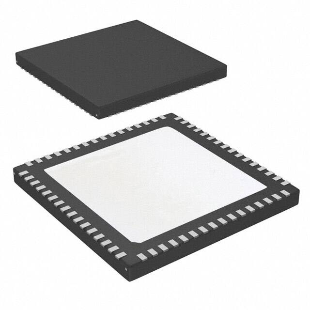


 工商网监
湘ICP备2023018690号
工商网监
湘ICP备2023018690号
