Si5395/94/92 Data Sheet
12-Channel, Any-Frequency, Any-Output Jitter Attenuator/Clock Multiplier with Ultra-Low Jitter
KEY FEATURES
The Si5395/94/92 Jitter attenuators combine fourth-generation DSPLL™ and MultiSynth™ technologies to deliver ultra-low jitter (69 fs) for high performance applications like 56G SerDes. They are used in applications that demand the highest level
of integration and jitter performance. All PLL components are integrated on-chip,
eliminating the risk of noise coupling associated with discrete solutions. Device
grades J/K/L/M/E have an integrated reference to save board space, improve system reliability and reduces the effect of acoustic emissions noise caused by temperature ramps. Grades A/B/C/D/P use an external crystal (XTAL) or crystal oscillator
(XO) reference.
• Generates any combination of output
frequencies from any input frequency
The Si5395/94/92 support free-run, synchronous and holdover modes as well as enhanced hitless switching, minimizing the phase transients associated when switching between input clocks. These devices are programmable via a serial interface
with in-circuit programmable non-volatile memory (NVM) so they always power up
with a known frequency configuration. Programming the Si5395/94/92 is easy with
Skyworks’ ClockBuilderTM Pro software. Factory preprogrammed devices are also
available.
• Input frequency range
• Differential: 8 kHz to 750 MHz
For more information, visit https://www.skyworksinc.com/en/Products/Timing page.
• Status monitoring
÷FRAC
÷FRAC
IN2
÷FRAC
IN3/FB_IN
÷FRAC
I2C/SPI
Status Monitor
Control
NVM
• LVCMOS: 8 kHz to 250 MHz
• Output frequency range
• Differential: 100 Hz to 1028 MHz
• LVCMOS: 100 Hz to 250 MHz
• Meets G.8262, E.8262.1 EEC Standards
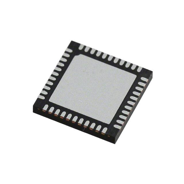
• Si5395: 4 input, 12 output (64-QFN/LGA)
• Si5392: 4 input, 2 output (44-QFN/LGA)
• External reference: Grades A/B/C/D/P
• Integrated reference: Grades J/K/L/M/E
• Drop-in compatible with Si5345/44/42
÷INT
OUT0A
MultiSynth
÷INT
OUT0
MultiSynth
÷INT
OUT1
MultiSynth
÷INT
OUT2
MultiSynth
÷INT
OUT3
MultiSynth
÷INT
OUT4
÷INT
OUT5
÷INT
OUT6
÷INT
OUT7
÷INT
OUT8
÷INT
OUT9
÷INT
OUT9A
Up to 12
Output Clocks
Si5395
Status Flags
DSPLL
• 100 fs RMS (fractional mode)
• Enhanced hitless switching minimizes output
phase transients (0.2 ns typ)
Si5394
IN1
4 Input
Clocks
• 85 fs RMS (integer mode)
Si5392
IN0
• 71 fs RMS (Grade E)
• Si5394: 4 input, 4 output (44-QFN/LGA)
Applications:
• 56G/112G PAM4 SerDes clocking
• OTN muxponders and transponders
• 10/40/100/200/400G networking line cards
• 10/40/100/400 GbE Synchronous Ethernet (ITU-T G.8262)
• Medical imaging
• Test and measurement
Integrated
Reference*
• Ultra low phase jitter:
• 69 fs RMS (Grade P)
*Only for Si539x J/K/L/M/E grades. Si539x A/B/C/D/P grades have external reference (XTAL or XO)
1
Skyworks Solutions, Inc. • Phone [781] 376-3000 • Fax [781] 376-3100 • sales@skyworksinc.com • www.skyworksinc.com
Rev. 1.2 • Skyworks Proprietary Information • Products and Product Information are Subject to Change Without Notice • December 4, 2021
1
�Si5395/94/92 Data Sheet • Features List
1. Features List
The Si5395/94/92 features are listed below:
• Generates any output frequency in any format from any input
frequency
• External XTAL or XO reference (A/B/C/D/P)
• Integrated reference (J/K/L/M/E)
• Ultra-low phase jitter of 69 fs (P-Grade)
• Dynamic phase adjust
• Input frequency range
• Differential: 8 kHz–750 MHz
• LVCMOS: 8 kHz–250 MHz
• Output frequency range
• Differential: 100 Hz to 1028 MHz
• LVCMOS: 100 Hz to 250 MHz
• Programmable jitter attenuation bandwidth: 0.1 Hz to 4 kHz
• Meets requirements of:
• ITU-T G.8262 (SyncE) EEC Options 1 and 2
• ITU-T G.8262.1 (Enhanced SyncE) eEEC
• Highly configurable outputs compatible with LVDS, LVPECL,
LVCMOS, CML, and HCSL with programmable signal amplitude
• Status monitoring (LOS, OOF, LOL)
• Enhanced hitless switching for 8 kHz, 19.44 MHz, 25 MHz
inputs and other frequencies
• Locks to gapped clock inputs
• Free-run and holdover modes
• Drop-in compatible with Si5345/44/42
2
•
•
•
•
•
Optional zero delay mode
Fast-lock acquisition for low nominal bandwidths
Independent Frequency-on-the fly for each MultiSynth
DCO mode: as low as 0.001 ppb step size
Core voltage
• VDD: 1.8 V ±5%
• VDDA: 3.3 V ±5%
• Independent output clock supply pins
• 3.3 V, 2.5 V, or 1.8 V
• Serial interface: I2C or SPI
• In-circuit programmable with non-volatile OTP memory
• ClockBuilder Pro software simplifies device configuration
• Si5395: 4 input, 12 output
• Grade A/B/C/D/P: 64-QFN 9×9 mm
• Grade J/K/L/M/E: 64-LGA 9x9 mm
• Si5394: 4 input, 4 output
• Grade A/B/C/D/P: 44-QFN 7×7 mm
• Grade J/K/L/M/E: 44-LGA 7x7 mm
• Si5392: 4 input, 2 output
• Grade A/B/C/D/P: 44-QFN 7×7 mm
• Grade J/K/L/M/E: 44-LGA 7x7 mm
• Temperature range: –40 to +85 °C
• Pb-free, RoHS-6 compliant
Skyworks Solutions, Inc. • Phone [781] 376-3000 • Fax [781] 376-3100 • sales@skyworksinc.com • www.skyworksinc.com
Rev. 1.2 • Skyworks Proprietary Information • Products and Product Information are Subject to Change Without Notice • December 4, 2021
2
�Si5395/94/92 Data Sheet • Related Documents
2. Related Documents
Table 2.1. Related Documentation and Software
Document/Resource
Description/URL
Si5395/94/92 Family Reference Manual
https://www.skyworksinc.com/-/media/Skyworks/SL/documents/public/reference-manuals/si5395-94-92-family.pdf
Crystal Reference Manual (Grades A/B/C/D/P only)
https://www.skyworksinc.com/-/media/Skyworks/SL/documents/public/reference-manuals/si534x-8x-9x-recommendedcrystals-rm.pdf
UG387: Si5392 Evaluation Board User's Guide
https://www.skyworksinc.com/-/media/Skyworks/SL/documents/public/user-guides/ug387-si5392-evb.pdf
UG334: Si5394 Evaluation Board User's Guide
https://www.skyworksinc.com/-/media/Skyworks/SL/documents/public/user-guides/ug334-si5394evb.pdf
UG335: Si5395 Evaluation Board User's Guide
https://www.skyworksinc.com/-/media/Skyworks/SL/documents/public/user-guides/ug335-si5395evb.pdf
AN1151: Using the Si539x in 56G SerDes Applications
AN1155: Differences between Si5342-47 and Si5392-97
https://www.skyworksinc.com/-/media/Skyworks/SL/documents/public/application-notes/an1151-using-si539x.pdf
https://www.skyworksinc.com/-/media/Skyworks/SL/documents/public/application-notes/an1151-using-si539x.pdf
AN1178: Frequency-On-the-Fly for Skyworks Jitter Attenuators
and Clock Generators
https://www.skyworksinc.com/-/media/Skyworks/SL/documents/public/application-notes/an1178-frequency-otf-jitter-attenclock-gen.pdf
Quality and Reliability
https://www.skyworksinc.com/Quality
Development Kits
https://www.skyworksinc.com/en/Products/Timing
ClockBuilder Pro (CBPro) Software
https://www.skyworksinc.com/en/Application-Pages/ClockbuilderPro-Software
3
Skyworks Solutions, Inc. • Phone [781] 376-3000 • Fax [781] 376-3100 • sales@skyworksinc.com • www.skyworksinc.com
Rev. 1.2 • Skyworks Proprietary Information • Products and Product Information are Subject to Change Without Notice • December 4, 2021
3
�Si5395/94/92 Data Sheet • Ordering Guide
3. Ordering Guide
Table 3.1. Si5395/94/92 A/B/C/D/P Ordering Guide (External Reference)
Ordering Part
Number (OPN)
Number of
Input/Output
Clocks
Output Clock
Frequency Range (MHz)
Supported Frequency
Synthesis Modes
Package
Reference
64-QFN
9×9 mm
External
44-QFN
7×7 mm
External
44-QFN
7×7 mm
External
Si5395
Si5395A-A-GM1, 2
0.0001 to 1028 MHz
Si5395B-A-GM1, 2
0.0001 to 350 MHz
Si5395C-A-GM1, 2
4/12
0.0001 to 1028 MHz
Si5395D-A-GM1, 2
0.0001 to 350 MHz
Si5395P-A-GM1, 2
Up to 3 domains
(Section 4.9.2 Grades P and E)
Integer and Fractional
Integer Only
Precision Calibration
Si5394
Si5394A-A-GM1, 2
0.0001 to 1028 MHz
Si5394B-A-GM1, 2
0.0001 to 350 MHz
Si5394C-A-GM1, 2
4/4
0.0001 to 1028 MHz
Si5394D-A-GM1, 2
0.0001 to 350 MHz
Si5394P-A-GM1, 2
Up to 2 domains
(Section 4.9.2 Grades P and E)
Integer and Fractional
Integer Only
Precision Calibration
Si5392
Si5392A-A-GM1, 2
0.0001 to 1028 MHz
Si5392B-A-GM1, 2
0.0001 to 350 MHz
Si5392C-A-GM1, 2
4/2
0.0001 to 1028 MHz
Integer and Fractional
Integer Only
Si5392D-A-GM1, 2
0.0001to 350 MHz
Si5392P-A-GM1, 2
1 domain
(Section 4.9.2 Grades P and E)
Precision Calibration
Si5395/94/92 Evaluation Board
Si5395A-A-EVB
12-output
Any-frequency, any Output
—
64-QFN
EVB
—
Si5395P-A-EVB
12-output
Low jitter clocks for 56G PAM4
SerDes
—
64-QFN
EVB
—
Si5394A-A-EVB
4-output
Any-frequency, any Output
—
44-QFN
EVB
—
Si5394P-A-EVB
4-output
Low jitter clocks for 56G PAM4
SerDes
—
44-QFN
EVB
—
Notes:
1. Add an R at the end of the OPN to denote tape and reel ordering options.
2. Custom, factory preprogrammed devices are available. Ordering part numbers are assigned by Skyworks and the ClockBuilder
Pro software utility. Custom part number format is “Si5395A-Axxxxx-GM” where “xxxxx” is a unique numerical sequence representing the preprogrammed configuration.
4
Skyworks Solutions, Inc. • Phone [781] 376-3000 • Fax [781] 376-3100 • sales@skyworksinc.com • www.skyworksinc.com
Rev. 1.2 • Skyworks Proprietary Information • Products and Product Information are Subject to Change Without Notice • December 4, 2021
4
�Si5395/94/92 Data Sheet • Ordering Guide
Table 3.2. Si5395/4/2 J/K/L/M/E Ordering guide (Integrated Reference)
Ordering Part
Number (OPN)
Number of
Input/Output
Clocks
Output Clock
Frequency Range (MHz)
Supported Frequency
Synthesis Modes
Package
Reference
64-LGA
9×9 mm
Internal
44-LGA
7×7 mm
Internal
44-LGA
7×7 mm
Internal
Si5395
Si5395J-A-GM1, 2
0.0001 to 1028 MHz
Si5395K-A-GM1, 2
0.0001 to 350 MHz
Si5395L-A-GM1, 2
4/12
0.0001 to 1028 MHz
Si5395M-A-GM1, 2
0.0001 to 350 MHz
Si5395E-A-GM1, 2
Up to 3 domains
(Section 4.9.2 Grades P and E)
Integer and Fractional
Integer Only
Precision Calibration
Si5394
Si5394J-A-GM1, 2
0.0001 to 1028 MHz
Si5394K-A-GM1, 2
0.0001 to 350 MHz
Si5394L-A-GM1, 2
4/4
0.0001 to 1028 MHz
Si5394M-A-GM1, 2
0.0001 to 350 MHz
Si5394E-A-GM1, 2
Up to 2 domains
(Section 4.9.2 Grades P and E)
Integer and Fractional
Integer Only
Precision Calibration
Si5392
Si5392J-A-GM1, 2
0.0001 to 1028 MHz
Si5392K-A-GM1, 2
0.0001 to 350 MHz
Si5392L-A-GM1, 2
4/2
0.0001 to 1028 MHz
Integer and Fractional
Integer Only
Si5392M-A-GM1, 2
0.0001to 350 MHz
Si5392E-A-GM1, 2
1 domain
(Section 4.9.2 Grades P and E)
Precision Calibration
Si5395/94/92 Evaluation Board
5
Si5395J-A-EVB
12-output
Any-frequency, any Output
—
64-LGA
EVB
—
Si5395E-A-EVB
12-output
Low jitter clocks for 56G PAM4
SerDes
—
64-LGA
EVB
—
Si5394J-A-EVB
4-output
Any-frequency, any Output
—
44-LGA
EVB
—
Si5394E-A-EVB
4-output
Low jitter clocks for 56G PAM4
SerDes
—
44-LGA
EVB
—
Si5392J-A-EVB
2-output
Any-frequency, any Output
—
44-LGA
EVB
—
Si5392E-A-EVB
2-output
Low jitter clocks for 56G PAM4
SerDes
—
44-LGA
EVB
—
Skyworks Solutions, Inc. • Phone [781] 376-3000 • Fax [781] 376-3100 • sales@skyworksinc.com • www.skyworksinc.com
Rev. 1.2 • Skyworks Proprietary Information • Products and Product Information are Subject to Change Without Notice • December 4, 2021
5
�Si5395/94/92 Data Sheet • Ordering Guide
Ordering Part
Number (OPN)
Number of
Input/Output
Clocks
Output Clock
Frequency Range (MHz)
Supported Frequency
Synthesis Modes
Package
Reference
Notes:
1. Add an R at the end of the OPN to denote tape and reel ordering options.
2. Custom, factory preprogrammed devices are available. Ordering part numbers are assigned by Skyworks and the ClockBuilder
Pro software utility. Custom part number format is “Si5395J-Axxxxx-GM” where “xxxxx” is a unique numerical sequence representing the preprogrammed configuration.
Figure 3.1. Ordering Part Number Fields
6
Skyworks Solutions, Inc. • Phone [781] 376-3000 • Fax [781] 376-3100 • sales@skyworksinc.com • www.skyworksinc.com
Rev. 1.2 • Skyworks Proprietary Information • Products and Product Information are Subject to Change Without Notice • December 4, 2021
6
�Table of Contents
1. Features List
. . . . . . . . . . . . . . . . . . . . . . . . . . . . . . . 2
2. Related Documents . . . . . . . . . . . . . . . . . . . . . . . . . . . . . 3
3. Ordering Guide
. . . . . . . . . . . . . . . . . . . . . . . . . . . . . . 4
4. Functional Description . . . . . . . . . . . . . . . . . . . . . . . . . . . . 9
4.1 Frequency Configuration
.
.
.
.
.
.
.
.
.
.
.
.
.
.
.
.
.
.
.
.
.
.
.
.
.
. 9
4.2 DSPLL Loop Bandwidth .
.
.
.
.
.
.
.
.
.
.
.
.
.
.
.
.
.
.
.
.
.
.
.
.
.
. 9
4.3 Fastlock Feature .
.
.
.
.
.
.
.
.
.
.
.
.
.
.
.
.
.
.
.
.
.
.
.
.
.
. 9
4.4 Modes of Operation . . . . .
4.4.1 Initialization and Reset . . .
4.4.2 Freerun Mode . . . . . .
4.4.3 Lock Acquisition Mode . . .
4.4.4 Locked Mode . . . . . .
4.4.5 Holdover Mode . . . . .
4.4.6 Frequency-on-the-Fly (FOTF)
.
.
.
.
.
.
.
.
.
.
.
.
.
.
.
.
.
.
.
.
.
.
.
.
.
.
.
.
.
.
.
.
.
.
.
.
.
.
.
.
.
.
.
.
.
.
.
.
.
.
.
.
.
.
.
.
.
.
.
.
.
.
.
.
.
.
.
.
.
.
.
.
.
.
.
.
.
.
.
.
.
.
.
.
.
.
.
.
.
.
.
.
.
.
.
.
.
.
.
.
.
.
.
.
.
.
.
.
.
.
.
.
.
.
.
.
.
.
.
.
.
.
.
.
.
.
.
.
.
.
.
.
.
.
.
.
.
.
.
.
.
.
.
.
.
.
.
.
.
.
.
.
.
.
. 9
.10
.10
.10
.10
.11
.11
4.5 Digitally Controlled Oscillator (DCO) Mode (Grade A/B/C/D and J/K/L/M ) .
.
.
.
.
.
.
.
.
.11
4.6 External Reference (Grade A/B/C/D/P Only) .
.
.
.
.
.
.
.
.
.12
4.7 Inputs (IN0, IN1, IN2, IN3) . . . . . . . . . . . . . . . . . .
4.7.1 Manual Input Selection (IN0, IN1, IN2, IN3) . . . . . . . . . . .
4.7.2 Automatic Input Selection (IN0, IN1, IN2, IN3) . . . . . . . . . .
4.7.3 Hitless Input Switching . . . . . . . . . . . . . . . . . .
4.7.4 Frequency Ramped Input Switching . . . . . . . . . . . . .
4.7.5 Glitchless Input Switching . . . . . . . . . . . . . . . . .
4.7.6 Synchronizing to Gapped Input Clocks (Grade A/B/C/D and J/K/L/M Only)
.
.
.
.
.
.
.
.
.
.
.
.
.
.
.
.
.
.
.
.
.
.
.
.
.
.
.
.
.
.
.
.
.
.
.
.
.
.
.
.
.
.
.
.
.
.
.
.
.
.12
.13
.13
.14
.15
.15
.16
4.8 Fault Monitoring . . .
4.8.1 Input LOS Detection.
4.8.2 XA/XB LOS Detection
4.8.3 OOF Detection . .
4.8.4 LOL Detection . . .
4.8.5 Interrupt Pin (INTRb)
.
.
.
.
.
.
.
.
.
.
.
.
.
.
.
.
.
.
.
.
.
.
.
.
.
.
.
.
.
.
.
.
.
.
.
.
.
.
.
.
.
.
.
.
.
.
.
.
.
.
.
.
.
.
.
.
.
.
.
.
.
.
.
.
.
.
.
.
.
.
.
.
.
.
.
.
.
.
.
.
.
.
.
.
.
.
.
.
.
.
.
.
.
.
.
.
.
.
.
.
.
.
.
.
.
.
.
.
.
.
.
.
.
.
.
.
.
.
.
.
.
.
.
.
.
.
.
.
.
.
.
.
.
.
.
.
.
.
.
.
.
.
.
.
.
.
.
.
.
.
.
.
.
.
.
.
.
.
.
.
.
.16
.17
.17
.17
.18
.19
.
.
.
.
.
.
.
.
.
.
.
.
.
.
.
.
.
.
.
.
.
.
.
.
.
.
.
.
.
.
.
.
.
.
.
.
.
.
.
.
.
.
.
.
.
.
.
.
.
.
.
.
.
.
.
.
.
.
.
.
.
.
.
.
.
.
.
.
.
.
.
.
.
.
.
.
.
.
.
.
.
.
.
.
.
.
.
.
.
.
.
.
.
.
.
.
.
.
.
.
.
.
.
.
.
.
.
.
.
.
.
.
.
.
.
.
.
.
.
.
.
.
.
.
.
.
.
.
.
.
.
.
.
.
.
.
.
.
.
.
.
.
.
.19
.19
.20
.21
.21
.21
.21
.21
.21
.21
.22
.22
.22
Skyworks Solutions, Inc. • Phone [781] 376-3000 • Fax [781] 376-3100 • sales@skyworksinc.com • www.skyworksinc.com
Rev. 1.2 • Skyworks Proprietary Information • Products and Product Information are Subject to Change Without Notice • December 4, 2021
7
4.9 Outputs . . . . . . . . . . . . . . . . . . . .
4.9.1 Grade A/B/C/D and J/K/L/M . . . . . . . . . . . .
4.9.2 Grades P and E . . . . . . . . . . . . . . . .
4.9.3 Output Crosspoint . . . . . . . . . . . . . . .
4.9.4 Output Signal Format . . . . . . . . . . . . . .
4.9.5 Programmable Common Mode Voltage For Differential Outputs
4.9.6 LVCMOS Output Impedance Selection . . . . . . . .
4.9.7 LVCMOS Output Signal Swing . . . . . . . . . . .
4.9.8 LVCMOS Output Polarity . . . . . . . . . . . . .
4.9.9 Output Enable/Disable . . . . . . . . . . . . . .
4.9.10 Output Driver State When Disabled . . . . . . . . .
4.9.11 Synchronous Output Disable Feature . . . . . . . .
4.9.12 Input/Output Skew Control . . . . . . . . . . . .
7
.
�4.9.13 Zero Delay Mode (Grades A/B/C/D and J/K/L/M )
4.9.14 Output Divider (R) Synchronization . . . . .
4.10 Power Management .
.
.
.
.
.
.
.
.
.
.
.
.
.
.
.
.
.
.
.
.
.
.
.
.
.
.
.
.
.
.
.22
.23
.
.
.
.
.
.
.
.
.
.
.
.
.
.
.
.
.
.
.
.
.
.
.
.
.
.
.23
4.11 In-Circuit Programming .
.
.
.
.
.
.
.
.
.
.
.
.
.
.
.
.
.
.
.
.
.
.
.
.
.
.23
4.12 Serial Interface
.
.
.
.
.
.
.
.
.
.
.
.
.
.
.
.
.
.
.
.
.
.
.
.
.
.23
4.13 Custom Factory Preprogrammed Parts .
.
.
.
.
.
.
.
.
.
.
.
.
.
.
.
.
.
.
.
.23
4.14 Register Map .
.
.
.
.
.
.
.
.
.
.
.
.
.
.
.
.
.
.
.
.23
5. Electrical Specifications . . . . . . . . . . . . . . . . . . . . . . . . . .
24
6. Typical Application Schematic . . . . . . . . . . . . . . . . . . . . . . . .
42
7. Detailed Block Diagrams . . . . . . . . . . . . . . . . . . . . . . . . . .
43
8. Typical Operating Characteristics
. . . . . . . . . . . . . . . . . . . . . .
44
9. Pin Descriptions . . . . . . . . . . . . . . . . . . . . . . . . . . . . .
46
10. Package Outlines . . . . . . . . . . . . . . . . . . . . . . . . . . . .
52
.
.
.
.
.
.
.
.
.
.
.
.
10.1 Si5395 A/B/C/D/P (External Reference) 9x9 mm 64-QFN Package Diagram .
.
.
.
.
.
.
.
.52
10.2 Si5395 J/K/L/M/E (Internal Reference) 9x9 mm 64-LGA Package Diagram .
.
.
.
.
.
.
.
.53
10.3 Si5394 and Si5392 A/B/C/D/P (External Reference) 7x7 mm 44-QFN Package Diagram
.
.
.
.54
10.4 Si5394 and Si5392 J/K/L/M/E (Internal Reference) 7x7 mm 44-LGA Package Diagram .
.
.
.
.55
11. PCB Land Pattern . . . . . . . . . . . . . . . . . . . . . . . . . . . .
57
12. Top Marking . . . . . . . . . . . . . . . . . . . . . . . . . . . . . .
59
13. Revision History. . . . . . . . . . . . . . . . . . . . . . . . . . . . .
60
Skyworks Solutions, Inc. • Phone [781] 376-3000 • Fax [781] 376-3100 • sales@skyworksinc.com • www.skyworksinc.com
Rev. 1.2 • Skyworks Proprietary Information • Products and Product Information are Subject to Change Without Notice • December 4, 2021
8
8
�Si5395/94/92 Data Sheet • Functional Description
4. Functional Description
The Si5392-95’s internal DSPLL provides jitter attenuation and any-frequency multiplication of the selected input frequency. Fractional
input dividers (P) allow the DSPLL to perform hitless switching between input clocks (INx) that are fractionally related. Input switching is
controlled manually or automatically using an internal state machine. The oscillator circuit (OSC) provides a frequency reference which
determines output frequency stability and accuracy while the device is in free-run or holdover mode. The high-performance MultiSynth
dividers (N) generate integer or fractionally related output frequencies for the output stage. A crosspoint switch connects any of the
MultiSynth generated frequencies to any of the outputs. Additional integer division (R) determines the final output frequency.
4.1 Frequency Configuration
The frequency configuration of the DSPLL is programmable through the serial interface and can also be stored in non-volatile memory.
The combination of fractional input dividers (Pn/Pd), fractional frequency multiplication (Mn/Md), fractional output MultiSynth division
(Nn/Nd), and integer output division (Rn) allows the generation of virtually any output frequency on any of the outputs. All divider values
for a specific frequency plan are easily determined using the ClockBuilder Pro utility.
4.2 DSPLL Loop Bandwidth
The DSPLL loop bandwidth determines the amount of input clock jitter attenuation. Register configurable DSPLL loop bandwidth
settings in the range of 0.1 Hz to 4 kHz are available for selection for Grade A/B/C/D. Since the loop bandwidth is controlled digitally,
the DSPLL will always remain stable with less than 0.1 dB of peaking regardless of the loop bandwidth selection. For grade P and E
devices, the DSPLL bandwidth is fixed at 100 Hz.
4.3 Fastlock Feature
Selecting a low DSPLL loop bandwidth (e.g. 0.1 Hz) will generally lengthen the lock acquisition time. The fastlock feature allows setting
a temporary Fastlock Loop Bandwidth that is used during the lock acquisition process. Higher fastlock loop bandwidth settings will
enable the DSPLLs to lock faster. Fastlock Loop Bandwidth settings of in the range of 100 Hz to 4 kHz are available for selection. The
DSPLL will revert to its normal loop bandwidth once lock acquisition has completed.
4.4 Modes of Operation
Once initialization is complete the DSPLL operates in one of four modes: Free-run Mode, Lock Acquisition Mode, Locked Mode, or
Holdover Mode. A state diagram showing the modes of operation is shown in the figure below. The following sections describe each of
these modes in greater detail.
Power-Up
Reset and
Initialization
No valid
input clocks
selected
Free-run
Valid input clock
selected
Lock Acquisition
(Fast Lock)
An input is
qualified and
available for
selection
No valid input
clocks available
for selection
Phase lock on
selected input
clock is achieved
Locked
Mode
Holdover
Mode
Input Clock
Switch
Selected input
clock fails
Yes
Yes
No
Holdover
History
Valid?
No
Other Valid
Clock Inputs
Available?
Figure 4.1. Modes of Operation
9
Skyworks Solutions, Inc. • Phone [781] 376-3000 • Fax [781] 376-3100 • sales@skyworksinc.com • www.skyworksinc.com
Rev. 1.2 • Skyworks Proprietary Information • Products and Product Information are Subject to Change Without Notice • December 4, 2021
9
�Si5395/94/92 Data Sheet • Functional Description
4.4.1 Initialization and Reset
Once power is applied, the device begins an initialization period, downloads default register values and configuration data from NVM,
and performs other initialization tasks. To communicate with the device through the serial interface, wait untl the initialization period is
complete. No clocks will be generated until the initialization is complete.
Clocks that feature the integrated crystal may require a slightly longer settling time compared to the external crystal device. See the
Reference Manual for more details.
Two types of resets are available. A hard reset is functionally similar to a device power-up. All registers will be restored to the values
stored in NVM and all circuits including the serial interface will be restored to their initial state. A hard reset is initiated using the RSTb
pin or by asserting the hard reset register bit.
A soft reset bypasses the NVM download. It is used to initiate register configuration changes.
4.4.2 Freerun Mode
The DSPLL will automatically enter freerun mode once power is applied to the device and initialization is complete. The frequency
accuracy of the generated output clocks in freerun mode is entirely dependent on the frequency accuracy of the external crystal or
reference clock on the XA/XB pins. For example, if the crystal frequency is ±100 ppm, then all the output clocks will be generated at
their configured frequency ±100 ppm in freerun mode. Any drift of the crystal frequency will be tracked at the output clock frequencies.
A TCXO or OCXO is recommended for applications that need better frequency accuracy and stability while in freerun or holdover
modes.
4.4.3 Lock Acquisition Mode
The device monitors all inputs for a valid clock. If at least one valid clock is available for synchronization, the DSPLL will automatically
start the lock acquisition process. If the fast lock feature is enabled, the DSPLL will acquire lock using the Fastlock Loop Bandwidth
setting and then transition to the DSPLL Loop Bandwidth setting when lock acquisition is complete. During lock acquisition the outputs
will generate a clock that follows the VCO frequency change as it pulls in to the input clock frequency.
4.4.4 Locked Mode
Once locked, the DSPLL will generate output clocks that are both frequency and phase locked to their selected input clocks. At this
point, any XTAL frequency drift will not affect the output frequency. A loss of lock pin (LOL) and status bit indicate when lock is
achieved. See 4.8.4 LOL Detection for more details on the operation of the loss-of-lock circuit.
10
Skyworks Solutions, Inc. • Phone [781] 376-3000 • Fax [781] 376-3100 • sales@skyworksinc.com • www.skyworksinc.com
Rev. 1.2 • Skyworks Proprietary Information • Products and Product Information are Subject to Change Without Notice • December 4, 2021
10
�Si5395/94/92 Data Sheet • Functional Description
4.4.5 Holdover Mode
The DSPLL will automatically enter holdover mode when the selected input clock becomes invalid and no other valid input clocks are
available for selection. The DSPLL uses an averaged input clock frequency as its final holdover frequency to minimize the disturbance
of the output clock phase and frequency when an input clock suddenly fails. The holdover circuit for the DSPLL stores up to 120
seconds of historical frequency data while locked to a valid clock input. The final averaged holdover frequency value is calculated from
a programmable window within the stored historical frequency data. Both the window size and the delay are programmable as shown in
the figure below. The window size determines the amount of holdover frequency averaging. The delay value allows ignoring frequency
data that may be corrupt just before the input clock failure.
Clock Failure and Entry
into Holdover
Historical Frequency Data Collected
time
120 seconds
Programmable historical data window used to
determine the final holdover value
Programmable delay
0
Figure 4.2. Programmable Holdover Window
When entering holdover, the DSPLL will pull its output clock frequency to the calculated averaged holdover frequency. While in
holdover, the output frequency drift is entirely dependent on the external crystal or external reference clock connected to the XA/XB
pins. If the clock input becomes valid, the DSPLL will automatically exit the holdover mode and re-acquire lock to the new input clock.
This process involves pulling the output clock frequency to achieve frequency and phase lock with the input clock. This pull-in process
is glitchless and its rate is controlled by the DSPLL or the Fastlock bandwidth.
The DSPLL output frequency when exiting holdover can be ramped (recommend). Just before the exit is initiated, the difference
between the current holdover frequency and the new desired frequency is measured. Using the calculated difference and a user-selectable ramp rate, the output is linearly ramped to the new frequency. The ramp rate can be 0.2 ppm/s, 40,000 ppm/s, or any of about 40
values in between. The DSPLL loop BW does not limit or affect ramp rate selections (and vice versa). CBPro defaults to ramped exit
from holdover. The same ramp rate settings are used for both exit from holdover and ramped input switching. For more information on
ramped input switching, see 4.7.4 Frequency Ramped Input Switching.
Note: If ramped holdover exit is not selected, the holdover exit is governed either by (1) the DSPLL loop BW or (2) a user-selectable
holdover exit BW.
4.4.6 Frequency-on-the-Fly (FOTF)
The Si5395/94/92 use register writes to support frequency-on-the-fly to allow frequency changes on one MultiSynth without affecting
the clocks generated from other MultiSynths. See the Si5395-94-92 Family Reference Manual and AN1178: Frequency-On-the-Fly for
Skyworks Jitter Attenuators and Clock Generators for more details.
4.5 Digitally Controlled Oscillator (DCO) Mode (Grade A/B/C/D and J/K/L/M )
The output MultiSynths support a DCO mode where their output frequencies are adjustable in predefined steps defined by frequency
step words (FSW). The frequency adjustments are controlled through the serial interface or by pin control using frequency increment
(FINC) or decrement (FDEC). A FINC will add the frequency step word to the DSPLL output frequency, while a FDEC will decrement
it. Any number of MultiSynths can be updated at once or independently controlled. The DCO mode is available when the DSPLL is
operating in either free-run or locked mode.
11
Skyworks Solutions, Inc. • Phone [781] 376-3000 • Fax [781] 376-3100 • sales@skyworksinc.com • www.skyworksinc.com
Rev. 1.2 • Skyworks Proprietary Information • Products and Product Information are Subject to Change Without Notice • December 4, 2021
11
�Si5395/94/92 Data Sheet • Functional Description
4.6 External Reference (Grade A/B/C/D/P Only)
An external crystal (XTAL) or crystal oscillator (XO) is used in combination with the internal oscillator (OSC) to produce an ultra low
jitter reference clock for the DSPLL and for providing a stable reference for the free-run and holdover modes. A simplified diagram is
shown in the figure below. The device includes internal XTAL loading capacitors which eliminates the need for external capacitors and
also has the benefit of reduced noise coupling from external sources. Refer to Table 5.12 External Crystal Specifications for Grades
A/B/C/D/P on page 39 for crystal specifications. For the A/B/C/D grades, a crystal in the range of 48 MHz to 54 MHz is recommended
for best jitter performance. The P grade devices must use a high quality 48 MHz crystal to achieve the ultra low jitter specification.
The family referernce manual provides additional information on PCB layout recommendations for the crystal to ensure optimum jitter
performance.
To achieve optimal jitter performance and minimize BOM cost, a crystal is recommended on the XA/XB reference input. For SyncE
pizza box applications (e.g. loop bandwidth set to 0.1 Hz), a TCXO is required on the XA/XB reference to minimize wander and to
provide a stable holdover reference. See the Si5395-94-92 Family Reference Manual for more information. Selection between the
external XTAL or REFCLK is controlled by register configuration. The internal crystal loading capacitors (CL) are disabled in the
REFCLK mode. Refer to Table 5.3 Input Clock Specifications on page 26 for REFCLK requirements when using this mode. A PREF
divider is available to accommodate external clock frequencies higher than 54 MHz. Frequencies in the range of 48 MHz to 54 MHz will
achieve the best output jitter performance.
25-54 MHz
XO/Clock
LVCMOS
25-54 MHz
XO/Clock
C1 is recommended
to increase the slew
rate at Xa
25-54 MHz
XTAL
X2
XB
XA
2xCL
C1
R1
See the Reference Manual for the
recommended R1, R2, C1 values
R2
Note: See Pin
Descriptions for
X1/X2 connections
nc
X1
XB
2xCL
2xCL
OSC
nc
X1
XA
2xCL
OSC
÷ PXAXB
Crystal Resonator
Connection
(Recommended)
nc
XB
X2
2xCL
nc
X1
XA
X2
2xCL
OSC
÷ PXAXB
Differential XO/Clock
Connection
(Not Recommended)
÷ PXAXB
LVCMOS XO/Clock
Connection
(Not Recommended)
Note: XA and XB must not exceed the maximum input voltage listed in Table 5.3 Input Clock Specifications on page 24
Figure 4.3. Crystal Resonator and External Reference Clock Connection Options
Note that connecting an external reference to a device that already has an integrated reference (grades J/K/L/M/E) is not allowed.
Doing so could lead to internal damage to the circuits.
4.7 Inputs (IN0, IN1, IN2, IN3)
There are four inputs that can be used to synchronize to the DSPLL. The inputs accept three formats of input clock: Standard
Differential/Single-Ended, Standard LVCMOS or Pulsed CMOS (See Family Reference Manual for more details). Input selection can be
manual (pin or register controlled) or automatic with user definable priorities.
12
Skyworks Solutions, Inc. • Phone [781] 376-3000 • Fax [781] 376-3100 • sales@skyworksinc.com • www.skyworksinc.com
Rev. 1.2 • Skyworks Proprietary Information • Products and Product Information are Subject to Change Without Notice • December 4, 2021
12
�Si5395/94/92 Data Sheet • Functional Description
4.7.1 Manual Input Selection (IN0, IN1, IN2, IN3)
Input clock selection can be made manually using the IN_SEL[1:0] pins or through a register. A register bit determines input selection
as pin selectable (default) or register selectable. If there is no clock signal on the selected input, the device will automatically enter
free-run or holdover mode. When the zero delay mode is enabled, IN3 becomes the feedback input (FB_IN) and is not available for
selection as a clock input.
Table 4.1. Manual Input Selection Using IN_SEL[1:0] Pins
Selected Input
IN_SEL[1:0]
Zero Delay Mode Disabled
Zero Delay Mode Enabled
0
0
IN0
IN0
0
1
IN1
IN1
1
0
IN2
IN2
1
1
IN3
Reserved
4.7.2 Automatic Input Selection (IN0, IN1, IN2, IN3)
An automatic input selection state machine is available in addition to the manual switching option. In automatic mode, the selection
criteria is based on input clock qualification, input priority, and the revertive option. Only input clocks that are valid can be selected
by the automatic clock selection state machine. If there are no valid input clocks available the DSPLL will enter the holdover mode.
With revertive switching enabled, the highest priority input with a valid input clock is always selected. If an input with a higher priority
becomes valid then an automatic switchover to that input will be initiated. With non-revertive switching, the active input will always
remain selected while it is valid. If it becomes invalid an automatic switchover to a valid input with the highest priority will be initiated.
13
Skyworks Solutions, Inc. • Phone [781] 376-3000 • Fax [781] 376-3100 • sales@skyworksinc.com • www.skyworksinc.com
Rev. 1.2 • Skyworks Proprietary Information • Products and Product Information are Subject to Change Without Notice • December 4, 2021
13
�Si5395/94/92 Data Sheet • Functional Description
4.7.3 Hitless Input Switching
Hitless switching is a feature that prevents a phase offset from propagating to the output when switching between two clock inputs that
have a fixed phase relationship. A hitless switch can only occur when the two input frequencies are frequency locked meaning that they
have to be exactly at the same frequency, or at an integer frequency relationship to each other. When hitless switching is enabled, the
DSPLL simply absorbs the phase difference between the two input clocks during a input switch. When disabled, the phase difference
between the two inputs is propagated to the output at a rate determined by the DSPLL Loop Bandwidth. The hitless switching feature
supports clock frequencies down to the minimum input frequency of 8 kHz; however, for optimum hitless switching performance, higher
input frequencies are recommended.
Figure 4.4. Output Phase Transient—Hitless Switching between Two 25 MHz Inputs (0 ppm, 180 Degree Phase Shift)
14
Skyworks Solutions, Inc. • Phone [781] 376-3000 • Fax [781] 376-3100 • sales@skyworksinc.com • www.skyworksinc.com
Rev. 1.2 • Skyworks Proprietary Information • Products and Product Information are Subject to Change Without Notice • December 4, 2021
14
�Si5395/94/92 Data Sheet • Functional Description
4.7.4 Frequency Ramped Input Switching
The ramped input switching feature is enabled/disabled depending on both the frequency of the Phase-Frequency detector (Fpfd) and
the difference in input frequencies (Zero-PPM vs non-zero PPM). The table below shows the selection criteria to enable ramped input
switching. The same ramp rate settings are used for both holdover exit and clock switching. For more information on ramped exit from
holdover, see 4.4.5 Holdover Mode and the Si5395-94-92 Family Reference Manual.
Figure 4.5. Output Frequency Transient—Ramped Switching between Two 8 kHz Inputs (±4.6 ppm Offset)
Table 4.2. Recommended Ramped Input Switching Settings for Internal Clock Switches
Maximum Input Frequency Difference
0 ppm Frequency Locked
≤ 10 ppm
> 10 ppm
Fpfd1 < 500 kHz
Fpfd1 ≥ 500 kHz
Ramped Exit from Holdover
Ramped Input Switching and Ramped Exit from Holdover
Ramped Exit from Holdover
Ramped Input Switching and Ramped Exit from Holdover
Note:
1. The Fpfd value is determineby various requirements of the frequency plan and is displayed in the CBPro project file.
Always enable hitless switching and enable phase buildout on holdover exit. See the latest version of CBPro to properly configure the
device.
.
4.7.5 Glitchless Input Switching
The glitchless switching feature allows the DSPLL to switch between two input clock frequencies that are up to ±500 ppm apart without
an abrupt phase change at the output. The DSPLL will pull-in to the new frequency using a ramped frequency step (if ramping is
enabled) or using Fastlock/nominal lock parameters (if ramping is disabled).
The loss of lock (LOL) indicator will assert while the DSPLL is pulling-in to the new clock frequency.
15
Skyworks Solutions, Inc. • Phone [781] 376-3000 • Fax [781] 376-3100 • sales@skyworksinc.com • www.skyworksinc.com
Rev. 1.2 • Skyworks Proprietary Information • Products and Product Information are Subject to Change Without Notice • December 4, 2021
15
�Si5395/94/92 Data Sheet • Functional Description
4.7.6 Synchronizing to Gapped Input Clocks (Grade A/B/C/D and J/K/L/M Only)
The DSPLL supports locking to an input clock that has missing periods. This is also referred to as a gapped clock. The purpose of
gapped clocking is to modulate the frequency of a periodic clock by selectively removing some of its cycles. Gapping a clock severely
increases its jitter so a phase-locked loop with high jitter tolerance and low loop bandwidth is required to produce a low-jitter periodic
clock. The resulting output will be a periodic non-gapped clock with an average frequency of the input with its missing cycles. For
example, an input clock of 100 MHz with one cycle removed every 10 cycles will result in a 90 MHz periodic non-gapped output clock.
This is shown in the following figure. For more information on gapped clocks, see “AN561: Introduction to Gapped Clocks and PLLs”.
Gapped Input Clock
Periodic Output Clock
100 MHz clock
1 missing period every 10
90 MHz non-gapped clock
100 ns
100 ns
DSPLL
1
2
3
4
5
6
7
8
9
1
10
Period Removed
10 ns
2
3
4
5
6
7
8
9
11.11111... ns
Figure 4.6. Generating an Averaged Clock Output Frequency from a Gapped Clock Input
A valid gapped clock input must have a minimum frequency of 10 MHz with a maximum of two missing cycles out of every eight.
Locking to a gapped clock will not trigger the LOS, OOF, and LOL fault monitors. Clock switching between gapped clocks may violate
the hitless switching specification in Table 5.8 Performance Characteristics on page 34 when the switch occurs during a gap in either
input clock.
4.8 Fault Monitoring
All four input clocks (IN0, IN1, IN2, IN3/FB_IN) are monitored for loss of signal (LOS) and out-of-frequency (OOF) as shown in the
figure below. The reference at the XA/XB pins is also monitored for LOS since it provides a critical reference clock for the DSPLL. There
is also a Loss Of Lock (LOL) indicator, which is asserted when the DSPLL loses synchronization.
XA XB
Si5395/94/92
OSC
IN0
IN0b
IN1
IN1b
IN2
IN2b
IN3/FB_IN
IN3/FB_INb
÷P0
LOS
OOF
Precision
Fast
÷P1
LOS
OOF
Precision
Fast
÷P2
LOS
OOF
Precision
Fast
÷P3
LOS
OOF
Precision
Fast
LOS
DSPLL
LOL
PD
LPF
÷M
Figure 4.7. Si5395/94/92 Fault Monitors
16
Skyworks Solutions, Inc. • Phone [781] 376-3000 • Fax [781] 376-3100 • sales@skyworksinc.com • www.skyworksinc.com
Rev. 1.2 • Skyworks Proprietary Information • Products and Product Information are Subject to Change Without Notice • December 4, 2021
16
�Si5395/94/92 Data Sheet • Functional Description
4.8.1 Input LOS Detection
The loss of signal monitor measures the period of each input clock cycle to detect phase irregularities or missing clock edges. Each of
the input LOS circuits has its own programmable sensitivity which allows ignoring missing edges or intermittent errors. Loss of signal
sensitivity is configurable using the ClockBuilder Pro utility. The LOS status for each of the monitors is accessible by reading a status
register. The live LOS register always displays the current LOS state and a sticky register always stays asserted until cleared. An option
to disable any of the LOS monitors is also available.
Monitor
Sticky
LOS
LOS
LOS
en
Live
Figure 4.8. LOS Status Indicators
4.8.2 XA/XB LOS Detection
A LOS monitor is available to ensure that the external crystal or reference clock is valid. By default the output clocks are disabled when
XAXB_LOS is detected. This feature can be disabled such that the device will continue to produce output clocks when XAXB_LOS is
detected.
4.8.3 OOF Detection
Each input clock is monitored for frequency accuracy with respect to a OOF reference which it considers as its “0_ppm” reference. This
OOF reference can be selected as either:
• XA/XB pins
• Any input clock (IN0, IN1, IN2, IN3)
The final OOF status is determined by the combination of both a precise OOF monitor and a fast OOF monitor as shown in the figure
below. An option to disable either monitor is also available. The live OOF register always displays the current OOF state, and its sticky
register bit stays asserted until cleared.
Monitor
OOF
Sticky
en
Precision
LOS
OOF
Fast
en
Live
Figure 4.9. OOF Status Indicator
17
Skyworks Solutions, Inc. • Phone [781] 376-3000 • Fax [781] 376-3100 • sales@skyworksinc.com • www.skyworksinc.com
Rev. 1.2 • Skyworks Proprietary Information • Products and Product Information are Subject to Change Without Notice • December 4, 2021
17
�Si5395/94/92 Data Sheet • Functional Description
4.8.3.1 Precision OOF Monitor
The precision OOF monitor circuit measures the frequency of all input clocks to within ±1/16 ppm accuracy with respect to the
selected OOF frequency reference. A valid input clock frequency is one that remains within the OOF frequency range which is register
configurable up to ±512 ppm in steps of 1/16 ppm. A configurable amount of hysteresis is also available to prevent the OOF status
from toggling at the failure boundary. An example is shown in the figure below. In this case, the OOF monitor is configured with a valid
frequency range of ±6 ppm and with 2 ppm of hysteresis. An option to use one of the input pins (IN0–IN3) as the 0 ppm OOF reference
instead of the XA/XB pins is available. This option is register configurable.
OOF Declared
fIN
Hysteresis
Hysteresis
OOF Cleared
-6 ppm
(Set)
-4 ppm
(Clear)
+4 ppm
(Clear)
0 ppm
+6 ppm
(Set)
OOF Reference
Figure 4.10. Example of Precise OOF Monitor Assertion and Deassertion Triggers
4.8.3.2 Fast OOF Monitor
Because the precision OOF monitor needs to provide 1/16 ppm of frequency measurement accuracy, it must measure the monitored
input clock frequencies over a relatively long period of time. This may be too slow to detect an input clock that is quickly ramping
in frequency. An additional level of OOF monitoring called the Fast OOF monitor runs in parallel with the precision OOF monitors to
quickly detect a ramping input frequency. The Fast OOF monitor asserts OOF on an input clock frequency that has changed by greater
than ±4000 ppm.
4.8.4 LOL Detection
The Loss Of Lock (LOL) monitor asserts a LOL register bit when the DSPLL has lost synchronization with its selected input clock.
There is also a dedicated loss of lock pin that reflects the loss of lock condition. The LOL monitor functions by measuring the frequency
difference between the input and feedback clocks at the phase detector. There are two LOL frequency monitors, one that sets the LOL
indicator (LOL Set) and another that clears the indicator (LOL Clear). An optional timer is available to delay clearing of the LOL indicator
to allow additional time for the DSPLL to completely lock to the input clock. The timer is also useful to prevent the LOL indicator from
toggling or chattering as the DSPLL completes lock acquisition. A block diagram of the LOL monitor is shown in the figure below. The
live LOL register always displays the current LOL state and a sticky register always stays asserted until cleared. The LOL pin reflects
the current state of the LOL monitor.
LOL Monitor
Sticky
LOL
Clear
Timer
LOL
Set
LOS
LOL
Live
LOLb
DSPLL
fIN
PD
Feedback
Clock
LPF
÷M
Si5395/94/92
Figure 4.11. LOL Status Indicators
The LOL frequency monitors have an adjustable sensitivity which is register configurable from 0.1 ppm to 10,000 ppm. Having two
separate frequency monitors allows for hysteresis to help prevent chattering of LOL status.
18
Skyworks Solutions, Inc. • Phone [781] 376-3000 • Fax [781] 376-3100 • sales@skyworksinc.com • www.skyworksinc.com
Rev. 1.2 • Skyworks Proprietary Information • Products and Product Information are Subject to Change Without Notice • December 4, 2021
18
�Si5395/94/92 Data Sheet • Functional Description
An example configuration where LOCK is indicated when there is less than 0.1 ppm frequency difference at the inputs of the phase
detector and LOL is indicated when there’s more than 1 ppm frequency difference is shown in the following figure.
Clear LOL
Threshold
Set LOL
Threshold
Lock Acquisition
LOL
Hysteresis
Lost Lock
LOCKED
0
0.1
1
10,000
Phase Detector Frequency Difference (ppm)
Figure 4.12. LOL Set and Clear Thresholds
An optional timer is available to delay clearing of the LOL indicator to allow additional time for the DSPLL to completely lock to the input
clock. The timer is also useful to prevent the LOL indicator from toggling or chattering as the DSPLL completes lock acquisition. The
configurable delay value depends on frequency configuration and loop bandwidth of the DSPLL and is automatically calculated using
the ClockBuilder Pro utility.
4.8.5 Interrupt Pin (INTRb)
An interrupt pin (INTRb) indicates a change in state of the status indicators (LOS, OOF, LOL, HOLD). Any of the status indicators are
maskable to prevent assertion of the interrupt pin. The state of the INTRb pin is reset by clearing the status register that caused the
interrupt.
4.9 Outputs
Each driver has a configurable voltage swing and common mode voltage covering a wide variety of differential signal formats. In
addition to supporting differential signals, any of the outputs can be configured as single-ended LVCMOS (3.3 V, 2.5 V, or 1.8 V)
providing up to 20 single-ended outputs, or any combination of differential and single-ended outputs.
4.9.1 Grade A/B/C/D and J/K/L/M
The Si539x "standard" grades A/B/C/D (external reference) and J/K/L/M (integrated reference) can generate any output frequency in
any format with best-in-class jitter. These devices are available as a preprogrammed option or can be written to the device via I2C. The
input/output frequency plan determines whether the output divider operates in integer or fractional mode. In the fractional mode, the
device can generate any output frequency or any format from any input frequency with best-in-class jitter. Some frequency plans allow
the user to use an integer mode that delivers even lower jitter. See the Si5395-94-92 Family Reference Manual for more details.
156.25 MHz
Backplane
Clock
19.44 MHz
Si5395A
Jitter
Attenuator
155.52 MHz
PHYs
PHYs
PHYs
PHYs
PHYs
PHYs
PHYs
PHYs
PHYs
PHYs
PHYs
PHYs
PHYs
PHYs
Figure 4.13. Si5395 A/B/C/D/J/K/L/M Jitter Attenuator
19
Skyworks Solutions, Inc. • Phone [781] 376-3000 • Fax [781] 376-3100 • sales@skyworksinc.com • www.skyworksinc.com
Rev. 1.2 • Skyworks Proprietary Information • Products and Product Information are Subject to Change Without Notice • December 4, 2021
19
�Si5395/94/92 Data Sheet • Functional Description
4.9.2 Grades P and E
Some applications, like 56G PAM4 SerDes, require even higher performance (< 100fs MAX) than is already provided by standard
Skyworks jitter attenuators (


 工商网监
湘ICP备2023018690号
工商网监
湘ICP备2023018690号

