SL28540
Low Power Clock Generator for Intel®Mobile Platform
Features
• 48 MHz USB clocks
• Compliant to Intel® CK540 UMPC clock spec
• Low power push-pull type differential output buffers
• Integrated voltage regulator
• Integrated series termination resistors on differential
clocks
• Scalable low voltage VDD_IO (3.3V to 1.05V)
• 8-step drive strength control for all single-ended clocks
• Differential CPU clocks with selectable frequency
• 100 MHz Differential SRC clocks
• 33 MHz PCI clocks
• Buffered Reference Clock 14.318 MHz
• Low-voltage frequency select input
• I2C support with readback capabilities
• Ideal Lexmark Spread Spectrum profile for maximum
electromagnetic interference (EMI) reduction
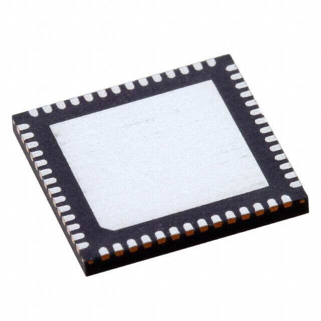
• 56-pin QFN (8x8) package
CPU
SRC
PCI
REF
x2 / x3
x7
x6
x1
DOT96 USB_48
x1
x1
• 96 MHz Differential DOT clock
Block Diagram
Pin Configuration
VDD_REF
Xin
Xout
14.318MHz
Crystal
REF
PLL Reference
VDD_CPU_I/O
CPU_STP#
CPUT[1:0]
CPUC[1:0]
PCI_STP#
CLKREQ#
CPU PLL1
SS
FS[C:A]
ITP_EN
CPU
SRC
CKPWRGD/PD#
PCI
GCLK_SEL
VDD_SRC_I/O
CPUT2_ITP/SRC8T
CPUC2_ITP/SRC8C
VDD_SRC_I/O
SRCT [2,3,4,11,7]
SRCC [2,3,4,11,7]
VDD_PCI
PCI[4:0], PCIF0
VDD_SRC_I/O
PLL3
SS
LCD_100T/SRC1T
LCD_100C/SRC1C
LCD_100
VDD_I/O
PLL2
Fixed
DOT96
DOT96T
DOT96C
VDD_48
USB_48
SDATA
SCLK
I2C
Logic
* internal Pull-up
** internal Pull-down
..................................................... Document #: Page 1 of 25
400 West Cesar Chavez, Austin, TX 78701
1+(512) 416-8500
1+(512) 416-9669
www.silabs.com
LCD
x1
�SL28540
Pin Definitions
Pin No.
Name
1
Xout
2
Xin
3
VDD_REF
4
Type
Description
O, SE 14.318 MHz Crystal output.
I
14.318 MHz Crystal input.
PWR
3.3V Power supply for outputs and maintains SMBUS registers during power
down.
REF0 / FSC / TEST_SEL
I/O
Fixed 14.318 clock output/3.3V-tolerant input for CPU frequency selection/
Selects test mode if pulled to VIHFS_C when CK_PWRGD is asserted HIGH.
Refer to DC Electrical Specifications table for VILFS_C, VIMFS_C, VIHFS_C specifications.
5
SDATA
I/O
SMBus compatible SDATA.
6
SCLK
I
7
PCI0 / CR#_A
8
VDD_PCI
9
PCI1 / CR#_B
I/O, SE 33 MHz Clock/3.3V Clock Request # Input
Mappable via I2C to control either SRC 1 or SRC 4. Default PCI1.
To configure this pin to serve as a Clock Request pin for either SRC pair 1 or pair
4 using the CR#_B_EN bit located in byte 5, bit 5, first disable PCI output (Hi-z) in
byte 2, bit 1.
0 = PCI1 enabled (default)
1= CR#_B enabled.
Byte 5, bit 4 controls whether CR#_B controls SRC1 or SRC4 pair
Byte 5, bit 4:
0 = CR#_B controls SRC1 pair (default)
1= CR#_B controls SRC4 pair
10
PCI2
O, SE 33 MHz Clock output/3.3V-tolerant input for enabling Trusted Mode
11
PCI3
O, SE 33 MHz Clock output
11, 12
PCI 4/GCLK_SEL
I/O, SE 33 MHz Clock output/3.3V-tolerant input for selecting clock source on pin 23,
PD
24.
Sampled at CKPWRGD assertion:
0 = SRC1(default), 1 = LCD_100M
Internal weak pull-down to GND
13
PCIF0 / ITP_EN
I/O, SE 33 MHz free running clock output/3.3V LVTTL input to enable SRC8 or
CPU2_ITP (sampled on the CKPWRGD assertion)
1 = CPU2_ITP, 0 = SRC8
SMBus compatible SCLOCK.
I/O, SE 33 MHz Clock/3.3V Clock Request # Input
Mappable via I2C to control either SRC 0 or SRC 2. Default PCI0.
To configure this pin to serve as a Clock Request pin for either SRC pair 2 or pair
0 using the CR#_A_EN bit located in byte 5 bit 7, first disable PCI output (Hi-z) in
byte 2, bit 1.
0 = PCI0 enabled (default)
1= CR#_A enabled.
Byte 5, bit 6 controls whether CR#_A controls SRC0 or SRC2 pair
Byte 5, bit 6:
0 = CR#_A controls SRC0 pair (default)
1= CR#_A controls SRC2 pair
PWR
3.3V power supply for PCI PLL
14
VSS_PCI
GND
Ground for outputs.
15
VDD_48
PWR
3.3V power supply for outputs and PLL.
16
USB_48 / FSA
17
VSS_48
GND
Ground for outputs.
18
VDD_IO
PWR
3.3V-1.05V power supply for outputs
19
DOT96T
O, DIF Fixed True 96 MHz clock output.
20
DOT96C
O, DIF Fixed complement 96 MHz clock output.
I/O
Fixed 48 MHz clock output/3.3V-tolerant input for CPU frequency selection
Refer to DC Electrical Specifications table for Vil_FS and Vih_FS specifications.
..................................................... Document #: Page 2 of 25
�SL28540
Pin Definitions (continued)
Pin No.
21
Name
VSS_IO
Type
Description
GND
Ground for outputs.
PWR
3.3V Power supply for PLL3.
22
VDD_PLL3
23
SRCT1 / LCDT_100
O, DIF True 100 MHz differential serial reference clock output/True 100 MHz LCD
video clock output
24
SRCC1 / LCDC_100
O, DIF Complementary 100 MHz differential serial reference clock output/Complementary 100 MHz LCD video clock output
25
VSS_PLL3
26
VDD_PLL3_IO
27
SRCT2
O, DIF True 100 MHz differential serial reference clock output.
O, DIF Complementary 100 MHz differential serial reference clock output.
GND
Ground for PLL3.
PWR
3.3V-1.05V power supply for outputs.
28
SRCC2
29
VSS_SRC
30
SRCT3 / CR#_C
I/O,
DIF
True 100 MHz differential serial reference clock output /3.3V Clock Request
#_C/D input
Selected via CR#_C_EN/CR#_D_EN bit located in byte 5 bit 3and 1.
The CR#_C_SEL and CR#_D_SEL bits in byte 5 bit 2 and 0 will select which SRC
to stop when asserted
31
SRCC3 / CR#_D
I/O,
DIF
Complementary 100 MHz differential serial reference clock output/3.3V Clock
Request #_C/D input
Selected via CR#_C_EN/CR#_D_EN bit located in byte 5 bit 3and 1.
The CR#_C_SEL and CR#_D_SEL bits in byte 5 bit 2 and 0 will select which SRC
to stop when asserted
32
VDD_SRC_IO
33
SRCT4
GND
PWR
Ground for outputs.
3.3V-1.05V Power supply for outputs.
O, DIF True 100 MHz differential serial reference clocks.
34
SRCC4
O, DIF Complementary 100 MHz differential serial reference clocks.
35
SRCT11
O, DIF True 100 MHz differential serial reference clocks.
O, DIF Complementary 100 MHz differential serial reference clocks.
36
SRCC11
37
CPU_STOP#
I
3.3V-tolerant input for stopping CPU outputs
During direct clock off to M1 mode transition, a serial load of BSEL data is driven
on CPU_STOP# and sampled on the rising edge of PCI_STOP#. See Figure 12
for more information.
38
PCI_STOP#
I
3.3V-tolerant input for stopping PCI and SRC outputs
During direct clock off to M1 mode transition, a serial load of BSEL data is driven
on CPU_STOP# and sampled on the rising edge of PCI_STOP#. See Figure 12
for more information.
39
VDD_SRC
PWR
3.3V power supply for SRC PLL.
40
VSS_SRC
GND
Ground for outputs.
41
SRCC7/ CR#_E
I/O,
DIF
Complementary 100 MHz differential serial reference clocks/3.3V CR#_E
Input.
Selected via CR#_E_EN/CR#_F_EN bit located in byte 6 bit 7 and 6.
When selected, CR#_E controls SRC6, CR#_F controls SRC8
42
SRCT7/ CR#_F
I/O,
DIF
True 100 MHz differential serial reference clocks/3.3V CR#_F Input.
Selected via CR#_E_EN/CR#_F_EN bit located in byte 6 bit 7 and 6.
When selected, CR#_E controls SRC6, CR#_F controls SRC8
43
VDD_SRC_IO
PWR
44
SRCC8 / CPUC2_ITP
O, DIF Selectable complementary differential CPU or SRC clock output.
ITP_EN = 0 @ CK_PWRGD assertion = SRC8
ITP_EN = 1 @ CK_PWRGD assertion = CPU2
45
SRCT8 / CPUT2_ITP,
O, DIF Selectable True differential CPU or SRC clock output.
ITP_EN = 0 @ CK_PWRGD assertion = SRC8
ITP_EN = 1 @ CK_PWRGD assertion = CPU2
46
NC
NC
3.3V-1.05V Power supply for outputs.
No connect.
..................................................... Document #: Page 3 of 25
�SL28540
Pin Definitions (continued)
Pin No.
Name
Type
PWR
Description
47
VDD_CPU_IO
48
CPUC1
O, DIF Complementary differential CPU clock outputs.
Note that CPU1 is the iAMT clock and is on in that mode.
49
CPUT1
O, DIF True differential CPU clock outputs.
Note that CPU1 is the iAMT clock and is on in that mode.
50
VSS_CPU
51
CPUC0
O, DIF Complement differential CPU clock outputs.
O, DIF True differential CPU clock outputs.
GND
3.3V-1.05V Power supply for outputs.
Ground for outputs.
52
CPUT0
53
VDD_CPU
54
CKPWRGD / PWRDWN#
I
3.3V LVTTL input. This pin is a level sensitive strobe used to latch the FS_A,
FS_B, FS_C, GLCK_SEL and ITP_EN.
After CKPWRGD (active HIGH) assertion, this pin becomes a real-time input for
asserting power down (active LOW).
55
FSB / TEST_MODE
I
3.3V-tolerant input for CPU frequency selection / Selects Ref/N or Tri-state
when in test mode.
0 = Tri-state, 1 = Ref/N
Refer to DC Electrical Specifications table for Vil_FS and Vih_FS specifications.
56
VSS_REF
PWR
GND
3.3V Power supply for CPU PLL.
Ground for outputs.
Table 1. Frequency Select Pin (FSA, FSB and FSC)
FSC
FSB
FSA
CPU
SRC
PCIF/PCI
REF
DOT96
USB
1
0
1
100 MHz
100 MHz
33 MHz
14.318 MHz
96 MHz
48 MHz
0
0
1
133 MHz
100 MHz
33 MHz
14.318 MHz
96 MHz
48 MHz
0
1
1
166 MHz
100 MHz
33 MHz
14.318 MHz
96 MHz
48 MHz
0
1
0
200 MHz
100 MHz
33 MHz
14.318 MHz
96 MHz
48 MHz
Apply the appropriate logic levels to FSA, FSB, and FSC
inputs before CK-PWRGD assertion to achieve host clock
frequency selection. When the clock chip sampled HIGH on
CK-PWRGD and indicates that VTT voltage is stable then
FSA, FSB, and FSC input values are sampled. This process
employs a one-shot functionality and once the CK-PWRGD
sampled a valid HIGH, all other FSA, FSB, FSC, and
CK-PWRGD transitions are ignored except in test mode
Serial Data Interface
To enhance the flexibility and function of the clock synthesizer,
a two-signal serial interface is provided. Through the Serial
Data Interface, various device functions, such as individual
clock output buffers are individually enabled or disabled. The
registers associated with the Serial Data Interface initialize to
their default setting at power-up. The use of this interface is
optional. Clock device register changes are normally made at
system initialization, if any are required. The interface cannot
be used during system operation for power management
functions.
Data Protocol
The clock driver serial protocol accepts byte write, byte read,
block write, and block read operations from the controller. For
block write/read operation, Access the bytes in sequential
order from lowest to highest (most significant bit first) with the
ability to stop after any complete byte is transferred. For byte
write and byte read operations, the system controller can
access individually indexed bytes. The offset of the indexed
byte is encoded in the command code described in Table 2.
The block write and block read protocol is outlined in Table 3
while Table 4 outlines byte write and byte read protocol. The
slave receiver address is 11010010 (D2h)
.
Table 2. Command Code Definition
Bit
7
(6:0)
Description
0 = Block read or block write operation, 1 = Byte read or byte write operation
Byte offset for byte read or byte write operation. For block read or block write operations, these bits should be '0000000'
..................................................... Document #: Page 4 of 25
�SL28540
Table 3. Block Read and Block Write Protocol
Block Write Protocol
Bit
1
8:2
9
10
18:11
19
27:20
28
36:29
37
45:38
Description
Start
Block Read Protocol
Bit
1
Slave address–7 bits
Write
8:2
9
Acknowledge from slave
Command Code–8 bits
10
18:11
Description
Start
Slave address–7 bits
Write
Acknowledge from slave
Command Code–8 bits
Acknowledge from slave
19
Acknowledge from slave
Byte Count–8 bits
20
Repeat start
Acknowledge from slave
Data byte 1–8 bits
Acknowledge from slave
Data byte 2–8 bits
27:21
Read = 1
29
Acknowledge from slave
37:30
46
Acknowledge from slave
....
Data Byte /Slave Acknowledges
....
Data Byte N–8 bits
....
Acknowledge from slave
....
Stop
Slave address–7 bits
28
38
46:39
47
55:48
Byte Count from slave–8 bits
Acknowledge
Data byte 1 from slave–8 bits
Acknowledge
Data byte 2 from slave–8 bits
56
Acknowledge
....
Data bytes from slave / Acknowledge
....
Data Byte N from slave–8 bits
....
NOT Acknowledge
....
Stop
Table 4. Byte Read and Byte Write Protocol
Byte Write Protocol
Bit
1
8:2
9
10
18:11
19
27:20
Description
Start
Slave address–7 bits
Write
Acknowledge from slave
Command Code–8 bits
Byte Read Protocol
Bit
1
8:2
9
10
18:11
Description
Start
Slave address–7 bits
Write
Acknowledge from slave
Command Code–8 bits
Acknowledge from slave
19
Acknowledge from slave
Data byte–8 bits
20
Repeated start
28
Acknowledge from slave
29
Stop
27:21
28
29
37:30
..................................................... Document #: Page 5 of 25
Slave address–7 bits
Read
Acknowledge from slave
Data from slave–8 bits
38
NOT Acknowledge
39
Stop
�SL28540
Control Registers
Byte 0: Control Register 0
Bit
@Pup
Name
Description
7
HW
FS_C
CPU Frequency Select Bit, set by HW
6
HW
FS_B
CPU Frequency Select Bit, set by HW
5
HW
FS_A
4
0
iAMT_EN
Set via SMBus or by combination of PWRDWN, CPU_STP, and PCI_STP
0 = Legacy Mode, 1 = iAMT Enabled
3
0
Reserved
Reserved
2
0
Reserved
Reserved
1
0
Reserved
Reserved
0
1
PD_Restore
CPU Frequency Select Bit, set by HW
Save Config. In powerdown
0 = Config. Cleared, 1 = Config. Saved
Byte 1: Control Register 1
Bit
@Pup
Name
Description
7
0
Reserved
6
0
PLL1_SS_DC
Reserved
Select for down or center SS
0 = Down spread, 1 = Center spread
5
0
PLL3_SS_DC
Select for down or center SS
0 = Down spread, 1 = Center spread
4
0
PLL3_CFB3
3
0
PLL3_CFB2
2
0
PLL3_CFB1
1
1
PLL3_CFB0
0
1
Reserved
SeeTable 8: PLL3 / SE configuration table
Reserved
Byte 2: Control Register 2
Bit
@Pup
Name
7
1
REF_OE
Output enable for REF
0 = Output Disabled, 1 = Output Enabled
Description
6
1
USB_OE
Output enable for USB
0 = Output Disabled, 1 = Output Enabled
5
1
PCIF0_OE
Output enable for PCIF0
0 = Output Disabled, 1 = Output Enabled
4
1
PCI4_OE
Output enable for PCI4
0 = Output Disabled, 1 = Output Enabled
3
1
PCI3_OE
Output enable for PCI3
0 = Output Disabled, 1 = Output Enabled
2
1
PCI2_OE
Output enable for PCI2
0 = Output Disabled, 1 = Output Enabled
1
1
PCI1_OE
Output enable for PCI1
0 = Output Disabled, 1 = Output Enabled
0
1
PCI0_OE
Output enable for PCI0
0 = Output Disabled, 1 = Output Enabled
Byte 3: Control Register 3
Bit
@Pup
Name
..................................................... Document #: Page 6 of 25
Description
�SL28540
Byte 3: Control Register 3
7
1
SRC[T/C]11_OE
Output enable for SRC11
0 = Output Disabled, 1 = Output Enabled
6
1
Reserved
Reserved
5
1
Reserved
Reserved
4
1
3
1
SRC[T/C]7_OE
2
1
Reserved
Reserved
1
1
Reserved
Reserved
0
1
SRC[T/C]4_OE
SRC[T/C]8/CPU2_ITP_OE Output enable for SRC8 or CPU2_ITP
0 = Output Disabled, 1 = Output Enabled
Output enable for SRC7
0 = Output Disabled, 1 = Output Enabled
Output enable for SRC4
0 = Output Disabled, 1 = Output Enabled
Byte 4: Control Register 4
Bit
@Pup
Name
7
1
SRC[T/C]3_OE
Output enable for SRC3
0 = Output Disabled, 1 = Output Enabled
Description
6
1
SRC[T/C]2_OE
Output enable for SRC2
0 = Output Disabled, 1 = Output Enabled
5
1
4
1
DOT96[T/C]_OE
Output enable for DOT96
0 = Output Disabled, 1 = Output Enabled
3
1
CPU[T/C]1_OE
Output enable for CPU1
0 = Output Disabled, 1 = Output Enabled
2
1
CPU[T/C]0_OE
Output enable for CPU0
0 = Output Disabled, 1 = Output Enabled
1
1
PLL1_SS_EN
Enable PLL1’s spread modulation,
0 = Spread Disabled, 1 = Spread Enabled
0
1
PLL3_SS_EN
Enable PLL3’s spread modulation
0 = Spread Disabled, 1 = Spread Enabled
SRC[T/C]1/LCD_100M[T/C] Output enable for SRC1/LCD_100M
_OE
0 = Output Disabled, 1 = Output Enabled
Byte 5: Control Register 5
Bit
@Pup
Name
Description
7
0
CR#_A_EN
Enable CR#_A (clk req)
0 = Disabled, 1 = Enabled,
6
0
CR#_A_SEL
Set CR#_A SRC0 or SRC2
0 = CR#_ASRC0, 1 = CR#_ASRC2
5
0
CR#_B_EN
Enable CR#_B(clk req)
0 = Disabled, 1 = Enabled,
4
0
CR#_B_SEL
Set CR#_B SRC1 or SRC4
0 = CR#_BSRC1, 1 = CR#_BSRC4
3
0
CR#_C_EN
Enable CR#_C (clk req)
0 = Disabled, 1 = Enabled
2
0
CR#_C_SEL
Set CR#_C SRC0 or SRC2
0 = CR#_CSRC0, 1 = CR#_CSRC2
1
0
CR#_D_EN
Enable CR#_D (clk req)
0 = Disabled, 1 = Enabled
0
0
CR#_D_SEL
Set CR#_D SRC1 or SRC4
0 = CR#_DSRC1, 1 = CR#_DSRC4
..................................................... Document #: Page 7 of 25
�SL28540
Byte 6: Control Register 6
Bit
@Pup
Name
7
0
CR#_E_EN
Enable CR#_E (clk req) SRC6
0 = Disabled, 1 = Enabled
Description
6
0
CR#_F_EN
Enable CR#_F (clk req) SRC8
0 = Disabled, 1 = Enabled
5
0
Reserved
Reserved
4
0
Reserved
Reserved
3
0
Reserved
Reserved
Reserved
2
0
Reserved
1
0
LCD_100_STP_CTRL
If set, LCD_100 stop with PCI_STOP#
0 = Free running, 1 = PCI_STOP# stoppable
0
0
SRC_STP_CTRL
If set, SRCs stop with PCI_STOP#
0 = Free running, 1 = PCI_STOP# stoppable
Byte 7: Vendor ID
Bit
@Pup
Name
7
0
Rev Code Bit 3
Revision Code Bit 3
Description
6
0
Rev Code Bit 2
Revision Code Bit 2
5
0
Rev Code Bit 1
Revision Code Bit 1
4
0
Rev Code Bit 0
Revision Code Bit 0
3
1
Vendor ID bit 3
Vendor ID Bit 3
2
0
Vendor ID bit 2
Vendor ID Bit 2
1
0
Vendor ID bit 1
Vendor ID Bit 1
0
0
Vendor ID bit 0
Vendor ID Bit 0
Byte 8: Control Register 8
Bit
@Pup
Name
Description
7
1
Device_ID3
6
0
Device_ID2
5
1
Device_ID1
4
0
Device_ID0
3
0
Reserved
Reserved
2
0
Reserved
Reserved
1
0
Reserved
Reserved
0
0
Reserved
Reserved
0000 = CK505 Yellow Cover Device, 56-pin TSSOP
0001 = CK505 Yellow Cover Device, 64-pin TSSOP
0010 = CK505 Yellow Cover Device, 48-pin QFN (Reserved)
0011 = CK505 Yellow Cover Device, 56-pin QFN (Reserved)
0100 = CK505 Yellow Cover Device, 64-pin QFN
0101 = CK505 Yellow Cover Device, 72-pin QFN (Reserved)
0110 = CK505 Yellow Cover Device, 48-pin SSOP (Reserved)
0111 = CK505 Yellow Cover Device, 56-pin SSOP (Reserved)
1000 = Reserved
1001 = Reserevd
1010 = CK505 Mobile
1011 = Reserved
1100 = Reserved
1101 = Reserved
1110 = Reserved
1111 = Reserved
Byte 9: Control Register 9
Bit
@Pup
Name
..................................................... Document #: Page 8 of 25
Description
�SL28540
Byte 9: Control Register 9
7
0
PCIF_0_with PCI_STOP# Allows control of PCIF_0 with assertion of PCI_STOP#
0 = Free running PCIF, 1 = Stopped with PCI_STOP#
6
HW
TME_STRAP
Trusted mode enable strap status
0 = Normal, 1 = No overclocking
5
1
REF drive strength
REF drive strength bit 1 (DSC 1)
0 = Low, 1 = High
See byte 13 for full-range setting
4
0
TEST_MODE_SEL
Mode select either REF/N or tri-state
0 = All output tri-state, 1 = All output REF/N
3
0
TEST_MODE_ENTRY
Allow entry into test mode
0 = Normal operation, 1 = Enter test mode
2
1
12C_VOUT
1
0
12C_VOUT
0
1
12C_VOUT
I2C_VOUT[2,1,0]
000 = 0.3V
001 = 0.4V
010 = 0.5V
011 = 0.6V
100 = 0.7V
101 = 0.8V (default)
110 = 0.9V
111 = 1.0V
Byte 10: Control Register 10
Bit
@Pup
Name
7
HW
GCLK_SEL latch
Description
6
0
PLL3_EN
PLL3 power down
0 = Power down, 1 = Power up
When GCLK_SEL=0, this bit is 0. When GCLK_SEL=1, this bit is 1.
5
1
PLL2_EN
PLL2 power down
0 = Power down, 1 = Power up
4
1
SRC_DIV_EN
SRC divider disable
0 = Disabled, 1 = Enabled
3
1
PCI_DIV_EN
PCI divider disable
0 = Disabled, 1 = Enabled
2
1
CPU_DIV_EN
CPU divider disable
0 = Disabled, 1 = Enabled
1
1
CPU1 Stop Enable
Enable CPU_STOP# control of CPU1
0 = Free running, 1= Stoppable
0
1
CPU0 Stop Enable
Enable CPU_STOP# control of CPU0
0 = Free running, 1= Stoppable
Readback of GCLK_SEL latch
0 = SRC1, 1 = LCD_100M
Byte 11: Control Register 11
Bit
@Pup
Name
7
0
Reserved
Reserved
Description
6
0
Reserved
Reserved
5
0
Reserved
Reserved
4
0
Reserved
Reserved
3
0
Reserved
Reserved
2
0
Reserved
Reserved
1
0
Reserved
Reserved
..................................................... Document #: Page 9 of 25
�SL28540
Byte 11: Control Register 11 (continued)
0
1
CPU[T/C]2
Allow control of CPU2 with assertion of CPU_STOP#
0 = Free running, 1 = Stopped with CPU_STOP#
Byte 12: Byte Count
Bit
@Pup
Name
7
0
Reserved
Description
6
0
Reserved
Reserved
5
0
BC5
Byte count
4
0
BC4
Byte count
3
1
BC3
Byte count
2
1
BC2
Byte count
1
0
BC1
Byte count
0
1
BC0
Byte count
Reserved
Byte 13: Control Register 13
Bit
@Pup
Name
7
0
PCI/PCIF drive strength
control bit 2
6
1
PCI/PCIF drive strength
control bit 1
DSC_2
DSC_1
DSC_0
5
1
PCI/PCIF drive strength
control bit 0
1
1
1
1
1
0
USB drive strength control
bit 2
1
0
1
1
0
0
Def ault PCI
0
1
1
Def ault REF/USB
0
1
0
0
0
1
0
0
0
4
3
2
0
1
0
USB drive strength control
bit 1
Description
Drive Strength Control table (DSC[2:0])
USB drive strength control
bit 0
1
0
REF drive strength control
bit 2
0
0
REF drive strength control
bit 0
Byte 14: Control Register 14
Bit
@Pup
Name
7
0
Reserevd
Description
6
0
Reserevd
5
0
PLL1 spread percentage
4
0
Reserevd
Reserved
3
0
Reserevd
Reserved
2
0
Reserevd
Reserved
1
0
Reserevd
Reserved
Reserved
Reserved
Select percentage of spread for PLL1
0 = 0.5%, 1=1%
................................................... Document #: Page 10 of 25
Buf f er
Strength
Strongest
Weakest
�SL28540
Byte 14: Control Register 14
Bit
@Pup
Name
0
1
SW_PCI
Description
SW PCI_STP# Function
0 = SW PCI_STP assert, 1 = SW PCI_STP deassert
When this bit is set to 0, all STOPPABLE PCI, PCIF and SRC outputs are
stopped in a synchronous manner with no short pulses.
When this bit is set to 1, all STOPPED PCI, PCIF and SRC outputs are
resumed in a synchronous manner with no short pulses.
Table 5. Crystal Recommendations
Frequency
(Fund)
Cut
Loading Load Cap
Drive
(max.)
Shunt Cap
(max.)
Motional
(max.)
Tolerance
(max.)
Stability
(max.)
Aging
(max.)
14.31818 MHz
AT
Parallel
0.1 mW
5 pF
0.016 pF
35 ppm
30 ppm
5 ppm
20 pF
The SL28540 requires a Parallel Resonance Crystal. Substituting a series resonance crystal causes the SL28540 to
operate at the wrong frequency and violates the ppm specification. For most applications there is a 300-ppm frequency
shift between series and parallel crystals due to incorrect
loading
C lo c k C h ip
C i2
C i1
P in
3 to 6 p
Crystal Loading
Crystal loading plays a critical role in achieving low ppm performance. To realize low ppm performance, use the total capacitance the crystal sees to calculate the appropriate capacitive
loading (CL).
X2
X1
C s1
C s2
T ra c e
2 .8 p F
XTAL
Figure 1 shows a typical crystal configuration using the two
trim capacitors. It is important that the trim capacitors are in
series with the crystal. It is not true that load capacitors are in
parallel with the crystal and are approximately equal to the
load capacitance of the crystal.
Ce1
Ce2
T r im
33pF
Figure 2. Crystal Loading Example
,
Use the following formulas to calculate the trim capacitor
values for Ce1 and Ce2.
Load Capacitance (each side)
Ce = 2 * CL – (Cs + Ci)
Total Capacitance (as seen by the crystal)
CLe
Figure 1. Crystal Capacitive Clarification
=
1
1
( Ce1 + Cs1
+ Ci1 +
1
Ce2 + Cs2 + Ci2
)
CL....................................................Crystal load capacitance
Calculating Load Capacitors
In addition to the standard external trim capacitors, consider
the trace capacitance and pin capacitance to calculate the
crystal loading correctly. Again, the capacitance on each side
is in series with the crystal. The total capacitance on both side
is twice the specified crystal load capacitance (CL). Trim
capacitors are calculated to provide equal capacitive loading
on both sides.
................................................... Document #: Page 11 of 25
CLe......................................... Actual loading seen by crystal
using standard value trim capacitors
Ce..................................................... External trim capacitors
Cs .............................................. Stray capacitance (terraced)
Ci ...........................................................Internal capacitance
(lead frame, bond wires, etc.)
�SL28540
PD_RESTORE
PWRDWN# (Power down) Assertion
If a ‘0’ is set for Byte 0 bit 0 then, upon assertion of PWRDWN#
LOW, the SL28540 initiates a full reset. The result of this is that
the clock chip emulates a cold power on start and goes to the
“Latches Open” state. If the PD_RESTORE bit is set to a ‘1’
then the configuration is stored upon PWRDWN# asserted
LOW. Note that if the iAMT bit, Byte 0 bit 3, is set to a ‘1’ then
the PD_RESTORE bit must be ignored. In other words, in Intel
iAMT mode, PWRDWN# reset is not allowed.
When PD is sampled HIGH by two consecutive rising edges
of CPUC, all single-ended outputs will be held LOW on their
next HIGH-to-LOW transition and differential clocks must held
LOW. When PD mode is desired as the initial power on state,
PD must be asserted HIGH in less than 10 s after asserting
CKPWRGD.
PWRDWN# (Power down) Clarification
The CKPWRGD/PWRDWN# pin is a dual-function pin. During
initial power up, the pin functions as CKPWRGD. Once
CKPWRGD has been sampled HIGH by the clock chip, the pin
assumes PD# functionality. The PD# pin is an asynchronous
active LOW input used to shut off all clocks cleanly before
shutting off power to the device. This signal is synchronized
internally to the device before powering down the clock
synthesizer. PD# is also an asynchronous input for powering
up the system. When PD# is asserted LOW, clocks are driven
to a LOW value and held before turning off the VCOs and the
crystal oscillator.
PWRDWN# Deassertion
The power up latency is less than 1.8 ms. This is the time from
the deassertion of the PD# pin or the ramping of the power
supply until the time that stable clocks are generated from the
clock chip. All differential outputs stopped in a three-state
condition, resulting from power down are driven high in less
than 300 s of PD# deassertion to a voltage greater than
200 mV. After the clock chip’s internal PLL is powered up and
locked, all outputs are enabled within a few clock cycles of
each clock. Figure 4 is an example showing the relationship of
clocks coming up.
PD#
CPUT, 133MHz
CPUC, 133MHz
SRCT 100MHz
SRCC 100MHz
USB, 48MHz
DOT96T
DOT96C
PCI, 33 MHz
REF
Figure 3. Power down Assertion Timing Waveform
Ts ta b le
< 1 .8 m s
PD#
C P U T , 1 3 3 MH z
C P U C , 1 3 3 MH z
S R C T 1 0 0 MH z
S R C C 1 0 0 MH z
U S B , 4 8 MH z
D OT 9 6 T
D OT 9 6 C
P C I, 3 3 MH z
REF
Td r iv e _ PW R D N #
2 00m V
Figure 4. Power down Deassertion Timing Waveform
................................................... Document #: Page 12 of 25
�SL28540
Figure 5. CKPWRGD Timing Diagram
................................................... Document #: Page 13 of 25
�SL28540
CPU_STP# Assertion
CPU_STP# Deassertion
The CPU_STP# signal is an active LOW input used for
synchronous stopping and starting the CPU output clocks
while the rest of the clock generator continues to function.
When the CPU_STP# pin is asserted, all CPU outputs that are
set with the SMBus configuration to be stoppable are stopped
within two to six CPU clock periods after sampled by two rising
edges of the internal CPUC clock. The final states of the
stopped CPU signals are CPUT = HIGH and CPUC = LOW.
The deassertion of the CPU_STP# signal causes all stopped
CPU outputs to resume normal operation in a synchronous
manner. No short or stretched clock pulses are produced when
the clock resumes. The maximum latency from the
deassertion to active outputs is no more than two CPU clock
cycles.
CPU_STP#
CPUT
CPUC
Figure 6. CPU_STP# Assertion Waveform
CPU_STP#
CPUT
CPUC
CPUT Internal
CPUC Internal
Tdrive_CPU_STP#,10 ns>200 mV
Figure 7. CPU_STP# Deassertion Waveform
1.8 ms
CPU_STOP#
PD#
CPUT(Free Running
CPUC(Free Running
CPUT(Stoppable)
CPUC(Stoppable)
DOT96T
DOT96C
Figure 8. CPU_STP# = Driven, CPU_PD = Driven, DOT_PD = Driven
................................................... Document #: Page 14 of 25
�SL28540
PCI_STP# Assertion
.
The PCI_STP# signal is an active LOW input used for
synchronously stopping and starting the PCI outputs while the
rest of the clock generator continues to function. The set-up
time for capturing PCI_STP# going LOW is 10 ns (tSU). (See
Figure 9.) The PCIF clocks are affected by this pin if their
corresponding control bit in the SMBus register is set to allow
them to be free running.
T su
PC I_STP#
PC I_F
PC I
SR C 100M H z
Figure 9. PCI_STP# Assertion Waveform
.
PCI_STP# Deassertion
The deassertion of the PCI_STP# signal causes all PCI and
stoppable PCIF clocks to resume running in a synchronous
manner within two PCI clock periods, after PCI_STP# transitions to a HIGH level.
T su
T drive_ S R C
P C I_S T P #
P C I_F
PCI
SR C 100 M H z
Figure 10. PCI_STP# Deassertion Waveform
.
Table 6. Output Driver Status during PCI-STOP# and CPU-STOP#
PCI_STOP# Asserted
Single-ended Clocks Stoppable
Differential Clocks
CPU_STOP# Asserted
Driven low
Running
Non stoppable
Running
Running
Stoppable
Clock driven high
Clock driven high
Clock# driven low
Clock# driven low
Running
Running
Non stoppable
SMBus OE Disabled
Driven low
Clock driven Low or 20K
pulldown
Table 7. Output Driver Status
All Single-ended Clocks
w/o Strap
All Differential Clocks except CPU1
w/ Strap
Clock
Clock#
CPU1
Clock
Clock#
Latches Open State
Low
Hi-Z
Low or 20K pulldown Low
Low or 20K
pulldown
Low
Powerdown
Low
Hi-Z
Low or 20K pulldown Low
Low or 20K
pulldown
Low
................................................... Document #: Page 15 of 25
�SL28540
.
Table 8. PLL3/SE Configuration Table
GCLK_SEL
B1b4
B1b3
B1b2
B1b1
Pin 23 (MHz)
Pin 24 (MHz)
0
0
0
0
0
0
0
0
0
1
0
0
1
0
0
1
0
1
0
Spread (%)
1
100
100
0.5
SRC1 from SRC_Main
1
0
100
100
0.5
LCD_100 from PLL3
1
1
100
100
1
LCD_100 from PLL3
1
0
0
100
100
1.5
LCD_100 from PLL3
1
0
1
100
100
2
LCD_100 from PLL3
PLL3 Disabled
Figure 11. Clock Generator Power up/Run State Diagram
................................................... Document #: Page 16 of 25
Comment
�SL28540
Absolute Maximum Conditions
Max.
Unit
VDD
Parameter
Core Supply Voltage
Description
Condition
Min.
4.6
V
VDD_A
Analog Supply Voltage
4.6
V
VDD_IO
IO Supply Voltage
3.8
V
VIN
Input Voltage
Relative to VSS
–0.5
4.6
V
TS
Temperature, Storage
Non-functional
–65
150
°C
TA
Temperature, Operating
Ambient
Functional
0
85
°C
TJ
Temperature, Junction
Functional
–
150
°C
ØJC
Dissipation, Junction to Case
Mil-STD-883E Method 1012.1
–
20
°C/W
–
60
°C/W
2000
–
V
ØJA
Dissipation, Junction to Ambient JEDEC (JESD 51)
ESDHBM
ESD Protection (Human Body
Model)
MIL-STD-883, Method 3015
UL-94
Flammability Rating
At 1/8 in.
MSL
Moisture Sensitivity Level
V–0
1
Multiple Supplies: The Voltage on any input or I/O pin cannot exceed the power pin during power-up. Power supply sequencing is NOT required.
DC Electrical Specifications
Parameter
Description
Condition
VDD core
3.3V Operating Voltage
3.3 ± 5%
VDD IO
3.3V Operating Voltage
3.3 ± 5%,
1.05V Operating Voltage
1.05V± 5%
Min.
Max.
Unit
3.135
3.465
V
3.135
3.465
V
0.9975
1.1025
V
VIH
3.3V Input High Voltage (SE)
2.0
VDD + 0.3
V
VIL
3.3V Input Low Voltage (SE)
VSS – 0.3
0.8
V
VIHI2C
Input High Voltage
SDATA, SCLK
2.2
–
V
VILI2C
Input Low Voltage
SDATA, SCLK
–
1.0
V
VIH_FS
FS_[A,B] Input High Voltage
0.7
VDD + 0.3
V
VIL_FS
FS_[A,B] Input Low Voltage
VSS – 0.3
0.35
V
VIHFS_C_TEST
FS_C Input High Voltage
VIMFS_C_NORMAL FS_C Input Middle Voltage
VILFS_C_NORMAL FS_C Input Low Voltage
IIH
Input High Leakage Current
Except internal pull-down resistors, 0 < VIN < VDD
2.0
VDD + 0.3
V
0.7
1.5
V
VSS – 0.3
0.35
V
–
5
A
IIL
Input Low Leakage Current
Except internal pull-up resistors, 0 < VIN < VDD
–5
–
A
VOH
3.3V Output High Voltage (SE)
IOH = –1 mA
2.4
–
V
IOL = 1 mA
VOL
3.3V Output Low Voltage (SE)
–
0.4
V
IOZ
High-impedance Output Current
–10
10
A
CIN
Input Pin Capacitance
1.5
5
pF
COUT
Output Pin Capacitance
6
pF
LIN
Pin Inductance
VXIH
Xin High Voltage
VXIL
IDD3.3V
IDD_IO
Dynamic IO Supply Current
40
mA
IDD_PWRDWN
Power down supply current
1
mA
–
7
nH
0.7VDD
VDD
V
Xin Low Voltage
0
0.3VDD
V
Dynamic Supply Current
–
1001
mA
1. All clock outputs are driving test case lump loads
................................................... Document #: Page 17 of 25
�SL28540
AC Electrical Specifications
Parameter
Description
Condition
Min.
Max.
Unit
47.5
52.5
%
69.841
71.0
ns
Crystal
TDC
XIN Duty Cycle
The device operates reliably with input
duty cycles up to 30/70 but the REF clock
duty cycle will not be within specification
TPERIOD
XIN Period
When XIN is driven from an external
clock source
TR/TF
XIN Rise and Fall Times
Measured between 0.3VDD and 0.7VDD
–
10.0
ns
TCCJ
XIN Cycle to Cycle Jitter
As an average over 1-s duration
–
500
ps
CPU at 0.8V
TDC
CPUT and CPUC Duty Cycle
Measured at 0V differential at 0.1s
45
55
%
TPERIOD
100 MHz CPUT and CPUC Period
Measured at 0V differential at 0.1s
9.99900
10.0010
ns
TPERIOD
133 MHz CPUT and CPUC Period
Measured at 0V differential at 0.1s
7.49925
7.50075
ns
TPERIOD
166 MHz CPUT and CPUC Period
Measured at 0V differential at 0.1s
5.99940
6.00060
ns
TPERIOD
200 MHz CPUT and CPUC Period
Measured at 0V differential at 0.1s
4.99950
5.00050
ns
TPERIODSS
100 MHz CPUT and CPUC Period, SSC Measured at 0V differential at 0.1s
10.02406
10.0261
ns
TPERIODSS
133 MHz CPUT and CPUC Period, SSC Measured at 0V differential at 0.1s
7.51805
7.51955
ns
TPERIODSS
166 MHz CPUT and CPUC Period, SSC Measured at 0V differential at 0.1s
6.01444
6.01564
ns
TPERIODSS
200 MHz CPUT and CPUC Period, SSC Measured at 0V differential at 0.1s
5.01203
5.01303
ns
TPERIODAbs
100 MHz CPUT and CPUC Absolute
period
Measured at 0V differential at 1 clock
9.91400
10.0860
ns
TPERIODAbs
133 MHz CPUT and CPUC Absolute
period
Measured at 0V differential at 1 clock
7.41425
7.58575
ns
TPERIODAbs
166 MHz CPUT and CPUC Absolute
period
Measured at 0V differential @ 1 clock
5.91440
6.08560
ns
TPERIODAbs
200 MHz CPUT and CPUC Absolute
period
Measured at 0V differential @ 1 clock
4.91450
5.08550
ns
TPERIODSSAbs 100 MHz CPUT and CPUC Absolute
period, SSC
Measured at 0V differential @ 1 clock
9.93906
10.1362
ns
TPERIODSSAbs 133 MHz CPUT and CPUC Absolute
period, SSC
Measured at 0V differential @ 1 clock
7.43305
7.62340
ns
TPERIODSSAbs 166 MHz CPUT and CPUC Absolute
period, SSC
Measured at 0V differential @ 1 clock
5.92944
6.11572
ns
TPERIODSSAbs 200 MHz CPUT and CPUC Absolute
period, SSC
Measured at 0V differential @ 1 clock
4.92703
5.11060
ns
–
85
ps
TCCJ
CPUT/C Cycle to Cycle Jitter
Measured at 0V differential
TCCJ2
CPU2_ITP Cycle to Cycle Jitter
Measured at 0V differential
–
125
ps
LACC
Long-term Accuracy
Measured at 0V differential
–
100
ppm
TSKEW
CPU1 to CPU0 Clock Skew
Measured at 0V differential
–
100
ps
TSKEW2
CPU2_ITP to CPU0 Clock Skew
Measured at 0V differential
–
150
ps
TR/TF
CPU Rising and Falling slew rate
Measured differentially from ±150 mV
2.5
8
V/ns
TRFM
Rise/Fall Matching
Measured single-endedly from ±75 mV
–
20
%
VHIGH
Voltage High
1.15
V
VLOW
Voltage Low
–0.3
–
V
VOX
Crossing Point Voltage at 0.7V Swing
300
550
mV
SRC at 0.8V
TDC
SRCT and SRCC Duty Cycle
Measured at 0V differential
TPERIOD
100 MHz SRC Period
Measured at 0V differential @ 0.1s
................................................... Document #: Page 18 of 25
45
55
%
9.99900
10.0010
ns
�SL28540
AC Electrical Specifications (continued)
Parameter
Description
Condition
Min.
Max.
Unit
10.02406
10.0261
ns
Measured at 0V differential @ 1 clock
9.8740
10.1260
ns
Measured at 0V differential @ 1 clock
9.89906
10.1762
ns
TPERIODSS
100 MHz SRC Period with Spread
enabled
Measured at 0V differential @ 0.1s
TPERIODAbs
100 MHz SRC Absolute Period
TPERIODSSAbs 100 MHz SRC Absolute Period with
Spread enbled
TCCJ
SRC Cycle to Cycle Jitter
Measured at 0V differential
–
125
ps
LACC
SRC Long Term Accuracy
Measured at 0V differential
–
100
ppm
TR / TF
SRC Rising and Falling slew rate
Measured differentially from ±150 mV
2.5
8
V/ns
TRFM
Rise/Fall Matching
Measured single-endedly from ±75 mV
–
20
%
VHIGH
Voltage High
1.15
V
VLOW
Voltage Low
–0.3
–
V
VOX
Crossing Point Voltage at 0.7V Swing
300
550
mV
DOT96 at 0.8V
TDC
DOT96T and DOT96C Duty Cycle
Measured at 0V differential
45
55
%
TPERIOD
DOT96T and DOT96C Period
Measured at 0V differential at 0.1s
10.4156
10.4177
ns
TPERIODAbs
DOT96T and DOT96C Absolute Period Measured at 0V differential at 0.1s
10.1656
10.6677
ns
TCCJ
DOT96 Cycle to Cycle Jitter
Measured at 0V differential at 1 clock
–
250
ps
LACC
DOT96 Long Term Accuracy
Measured at 0V differential at 1 clock
–
100
ppm
TR / TF
DOT96 Rising and Falling slew rate
Measured differentially from ±150 mV
2.5
8
V/ns
TRFM
Rise/Fall Matching
Measured single-endedly from ±75 mV
–
20
%
VHIGH
Voltage High
1.15
V
VLOW
Voltage Low
–0.3
–
V
VOX
Crossing Point Voltage at 0.7V Swing
300
550
mV
45
55
%
LCD_100_SSC at 0.8V
TDC
LCD_100 Duty Cycle
Measured at 0V differential
TPERIOD
LCD_100 Period
Measured at 0V differential at 0.1s
9.99900
10.0010
ns
TPERIODSS
LCD_100 Period with -0.5% Spread
Measured at 0V differential at 0.1s
10.02406
10.0261
ns
TPERIODAbs
LCD_100 Absolute Period
TPERIODSSAbs LCD_100 Absolute Period, SSC
Measured at 0V differential at 1 clock
9.874
10.0860
ns
Measured at 0V differential @ 1 clock
9.89906
10.1762
ns
TCCJ
LCD_100 Cycle to Cycle Jitter
Measured at 0V differential
–
250
ps
LACC
LCD_100 Long Term Accuracy
Measured at 0V differential
–
100
ppm
TR / TF
LCD_100 Rising and Falling slew rate
Measured differentially from ±150 mV
2.5
8
V/ns
TRFM
Rise/Fall Matching
Measured single-endedly from ±75 mV
–
20
%
VHIGH
Voltage High
1.15
V
VLOW
Voltage Low
–0.3
–
V
VOX
Crossing Point Voltage at 0.7V Swing
300
550
mV
PCI/PCIF at 3.3V
TDC
PCI Duty Cycle
Measurement at 1.5V
45
55
%
TPERIOD
Spread Disabled PCIF/PCI Period
Measurement at 1.5V
29.99100
30.00900
ns
TPERIODSS
Spread Enabled PCIF/PCI Period
Measurement at 1.5V
29.99100
30.15980
ns
TPERIODAbs
Spread Disabled PCIF/PCI Period
Measurement at 1.5V
29.49100
30.50900
ns
TPERIODSSAbs Spread Enabled PCIF/PCI Period
Measurement at 1.5V
29.49100
30.65980
ns
THIGH
Pread enabled PCIF and PCI high time Measurement at 2.0V
12
ns
TLOW
Spread enabled PCIF and PCI low time Measurement at 0.8V
12
ns
................................................... Document #: Page 19 of 25
�SL28540
AC Electrical Specifications (continued)
Parameter
Description
Condition
Min.
Max.
Unit
1.0
4.0
V/ns
Measurement at 1.5V
–
1000
ps
Measurement at 1.5V
–
500
ps
Measurement at 1.5V
–
300
ppm
T R / TF
PCIF/PCI rising and falling Edge Rate
Measured between 0.8V and 2.0V
TSKEW
Any PCI clock to Any PCI clock Skew
TCCJ
PCIF and PCI Cycle to Cycle Jitter
LACC
PCIF/PCI Long Term Accuracy
48_M at 3.3V
TDC
Duty Cycle
Measurement at 1.5V
45
55
%
TPERIOD
Period
Measurement at 1.5V
20.83125
20.83542
ns
TPERIODAbs
Absolute Period
Measurement at 1.5V
20.48125
21.18542
ns
THIGH
48_M High time
Measurement at 2.0V
8.216563
11.15198
ns
TLOW
48_M Low time
Measurement at 0.8V
7.694
9.836
ns
T R / TF
Rising and Falling Edge Rate
Measured between 0.8V and 2.0V
1.0
2.0
V/ns
TCCJ
Cycle to Cycle Jitter
Measurement at 1.5V
–
350
ps
LACC
48M Long Term Accuracy
Measurement at 1.5V
–
100
ppm
TDC
REF Duty Cycle
Measurement at 1.5V
45
55
%
REF
TPERIOD
REF Period
Measurement at 1.5V
69.82033
69.86224
ns
TPERIODAbs
REF Absolute Period
Measurement at 1.5V
68.83429
70.86224
ns
T R / TF
REF Rising and Falling Edge Rate
Measured between 0.8V and 2.0V
1.0
4.0
V/ns
TSKEW
REF Clock to REF Clock
Measurement at 1.5V
–
500
ps
TCCJ
REF Cycle to Cycle Jitter
Measurement at 1.5V
–
1000
ps
LACC
Long Term Accuracy
Measurement at 1.5V
–
300
ppm
–
1.8
ms
10.0
–
ns
ENABLE/DISABLE and SET-UP
TSTABLE
Clock Stabilization from Power-up
TSS
Stopclock Set-up Time
Test and Measurement Set-up
For PCI Single-ended Signals and Reference
The following diagram shows the test load configurations for
the single-ended PCI, USB, and REF output signals.
L1
22
50
PCI/USB
L1 = 0.5", L2 = 4"
L1
22
Measurement
Point
L2
4 pF
Measurement
Point
50
L2
4 pF
Figure 12. Single-ended PCI and USB Double Load Configuration
................................................... Document #: Page 20 of 25
�SL28540
L1
15
L2
50
REF
Measurement
Point
4 pF
L1
15
L2
50
Measurement
Point
4 pF
L1
15
L2
50
Measurement
Point
4 pF
Figure 13. Single-ended REF Triple Load Configuration
Figure 14. Single-ended Output Signals (for AC Parameters Measurement)
For CPU, SRC, and DOT96 Signals and Reference
This diagram shows the test load configuration for the differential CPU and SRC outputs
Figure 15. 0.7V Differential Load Configuration
................................................... Document #: Page 21 of 25
�SL28540
Clock Period (Differential)
Positive Duty Cycle (Differential)
Negative Duty Cycle (Differential)
0.0V
0.0V
Clck-Clck#
Rise
Edge
Rate
Fall
Edge
Rate
VIH = +150V
VIH = +150V
0.0V
0.0V
VIL = -150V
VIL = -150V
Clock-Clock#
Figure 16. Differential Measurement for Differential Output Signals (for AC Parameters Measurement)
V MAX = 1.15V
V MAX = 1.15V
CLK#
Vcross MAX = 550mV
Vcross MAX = 550mV
Vcross MIN = 300mV
Vcross MIN = 300mV
CLK
V MIN = 0.30V
V MIN = 0.30V
CLK#
Vcross delta = 140mV
Vcross delta = 140mV
CLK#
Vcross median +75mV
Vcross median
Vcross m edian -75m V
CLK
ise
Tr
Vcross median
Tf
al
l
CLK#
CLK
Figure 17. Single-ended Measurement for Differential Output Signals (for AC Parameters Measurement)
................................................... Document #: Page 22 of 25
�SL28540
Ordering Information
Part Number
Package Type
Product Flow
Lead-free
SL28540ALC
56-pin QFN
Commercial, 0 to 85C
SL28540ALCT
56-pin QFN, Tape and Reel
Commercial, 0 to 85C
................................................... Document #: Page 23 of 25
�SL28540
Package Diagrams
56-Lead QFN 8x 8mm LF56A
TOP VIEW
BOTTOM VIEW
SIDE VIEW
0.08[0.003]
C
1.00[0.039] MAX.
7.90[0.311]
8.10[0.319]
A
0.05[0.002] MAX.
0.80[0.031] MAX.
7.70[0.303]
7.80[0.307]
0.18[0.007]
0.28[0.011]
0.20[0.008] REF.
0.80[0.031]
DIA.
PIN1 ID
0.20[0.008] R.
N
N
1
1
2
2
0.45[0.018]
6.45[0.254]
6.55[0.258]
7.90[0.311]
8.10[0.319]
7.70[0.303]
7.80[0.307]
E-PAD
(PAD SIZE VARY
BY DEVICE TYPE)
0.30[0.012]
0.50[0.020]
0°-12°
0.50[0.020]
C
SEATING
PLANE
0.24[0.009]
0.60[0.024]
6.45[0.254]
6.55[0.258]
51-85215-**
................................................... Document #: Page 24 of 25
(4X)
�SL28540
Document History Page
Document Title: SL28540 Low Power Clock Generator for Intel®Mobile Platform
Document Number:
REV.
Issue Date
Orig. of
Change
1.0
03/19/2007
SLI
New data sheet
1.1
08/15/2007
SLI
Updated Features list
Updated DC Electrical Specifications table
Updated AC Electrical Specifications table
Updated ordering information
1.2
09/15/2008
JMA
1. Added iAMT functions
2. Removed TME definition
Description of Change
The information in this document is believed to be accurate in all respects at the time of publication but is subject to change without notice. Silicon Laboratories assumes no responsibility for errors and omissions, and disclaims responsibility for any consequences resulting from the use
of information included herein. Additionally, Silicon Laboratories assumes no responsibility for the functioning of undescribed features or
parameters. Silicon Laboratories reserves the right to make changes without further notice. Silicon Laboratories makes no warranty, representation or guarantee regarding the suitability of its products for any particular purpose, nor does Silicon Laboratories assume any liability arising
out of the application or use of any product or circuit, and specifically disclaims any and all liability, including without limitation consequential or
incidental damages. Silicon Laboratories products are not designed, intended, or authorized for use in applications intended to support or sustain life, or for any other application in which the failure of the Silicon Laboratories product could create a situation where personal injury or
death may occur. Should Buyer purchase or use Silicon Laboratories products for any such unintended or unauthorized application, Buyer
shall indemnify and hold Silicon Laboratories harmless against all claims and damages.
................................................... Document #: Page 25 of 25
�


 工商网监
湘ICP备2023018690号
工商网监
湘ICP备2023018690号
