SL28779
EProClock® Generator for Intel Calpella Chipset
Features
• 96MHz Differential DOT clock
• 27MHz Video clock
• Intel CK505 Clock Revision 1.0 Compliant
• Hybrid Video Support - Simultaneous DOT96,
27MHz_SS and 27MHz_NSS video clocks
• 48MHz USB clock
• Buffered Reference Clock 14.318MHz
• PCI-Express Gen 2 Compliant
• 14.318MHz Crystal Input or Clock input
• Low power push-pull type differential output buffers
• EProClock® Programmable Technology
• Integrated voltage regulator
• I2C support with readback capabilities
• Integrated resistors on differential clocks
• Triangular Spread Spectrum profile for maximum
electromagnetic interference (EMI) reduction
• Scalable low voltage VDD_IO (3.3V to 1.05V)
• 3.3V Power supply
• Wireless friendly 3-bits slew rate control on
single-ended clocks.
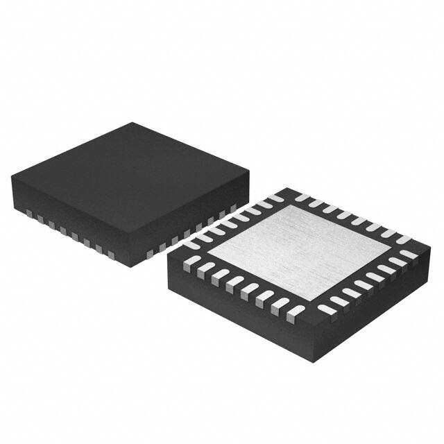
• 32-pin QFN package
• Differential CPU clocks with selectable frequency
• 100MHz Differential SRC clocks
CPU
SRC
x2
x1
SATA DOT96 USB_48 REF 27M
x1
x1
x1
x1
x2
• 100MHz Differential SATA clocks
Pin Configuration
Block Diagram
** Internal 100K-ohm Pull-Down Resistor
DOC#: SP-AP-0066 (Rev. AA)
400 West Cesar Chavez, Austin, TX 78701
1+(512) 416-8500
1+(512) 416-9669
Page 1 of 22
www.silabs.com
�SL28779
32-QFN Pin Definitions
Pin No.
1
Name
VDD_DOT
Type
PWR
Description
3.3V Power supply for outputs and PLL
2
VSS_DOT
3
DOT96
O, DIF Fixed true 96MHz clock output
GND
Ground for outputs
4
DOT96#
O, DIF Fixed complement 96MHz clock output
5
VDD_27
PWR
3.3V Power supply for 27MHz PLL
Non-spread 27MHz video clock output
6
27M_NSS
O,SE
7
27M_SS
O, SE Spread 27MHz video clock output
8
USB_48
O,SE
Non-spread 48MHz video clock output
9
VSS_27
GND
Ground for 27MHz PLL
10
SRC0 / SATA
O, DIF 100MHz True differential serial reference clock
11
SRC0# / SATA#
O, DIF 100MHz Complement differential serial reference clock
12
VSS_SRC
13
SRC1
O, DIF 100MHz True differential serial reference clock
GND
14
SRC1#
O, DIF 100MHz Complement differential serial reference clock
15
VDD_SRC_IO
16
27_OE#
17
VDD_SRC
18
VDD_CPU_IO
19
CPU1#
O, DIF Complement differential CPU clock output
20
CPU1
O, DIF True differential CPU clock output
21
VSS_CPU
22
CPU0#
O, DIF Complement differential CPU clock output
23
CPU0
O, DIF True differential CPU clock output
24
VDD_CPU
25
CKPWRGD/PD#
PWR
I
Ground for PLL
Scalable 3.3V to 1.05V power supply for output buffer
3.3V tolerance input pin to enable and disable both 27_NSS and 27_SS
PWR
3.3V Power supply for PLL
PWR
Scalable 3.3V to 1.05V power supply for output buffer
GND
PWR
I
Ground for PLL
3.3V Power supply for CPU PLL
3.3V LVTTL input. This pin is a level sensitive strobe used to latch the FS.
After CKPWRGD (active HIGH) assertion, this pin becomes a real-time input for
asserting power down (active LOW)
26
VSS_REF
GND
27
XOUT
O, SE 14.318MHz Crystal output, Float XOUT if using only CLKIN (Clock input)
28
XIN/CLKIN
I
29
VDD_REF
PWR
30
REF/FS**
14.318MHz Crystal input or 3.3V, 14.318MHz Clock Input
3.3V Power supply for outputs and also maintains SMBUS registers during
power-down
PD, I/O 3.3V tolerant input for Graphic clock selection/fixed 14.318MHz clock output.
(Internal 100K-ohm pull-down resistor on FS pin)
Refer to DC Electrical Specifications table for Vil_FS and Vih_FS specifications
31
SDATA
I/O
32
SCLK
I
DOC#: SP-AP-0066 (Rev. AA)
Ground for outputs
SMBus compatible SDATA
SMBus compatible SCLOCK
Page 2 of 22
�SL28779
PC EProClock® Programmable Technology
PC EProClock® is the world’s first non-volatile programmable
PC clock. The PC EProClock® technology allows board
designer to promptly achieve optimum compliance and clock
signal integrity; historically, attainable typically through device
and/or board redesigns.
PC EProClock® technology can be configured through SMBus
or hard coded.
- Differential skew control on true or compliment or both
- Differential duty cycle control on true or compliment or both
- Differential amplitude control
- Differential and single-ended slew rate control
Features:
- Program Internal or External series resistor on single-ended
clocks
- > 4000 bits of configurations
- Program different spread profiles
- Can be configured through SMBus or hard coded
- Program different spread modulation rate
- Custom frequency sets
Frequency Select Pin (FS)
FS
CPU
Power On
0
133MHz
Default
1
100MHz
SRC
SATA
DOT96
USB_48
27MHz
REF
100MHz
100MHz
96MHz
48MHz
27MHz
14.318MHz
Frequency Select Pin FS
Apply the appropriate logic levels to FS inputs before
CKPWRGD assertion to achieve host clock frequency
selection. When the clock chip sampled HIGH on CKPWRGD
and indicates that VTT voltage is stable then FS input values
are sampled. This process employs a one-shot functionality
and once the CKPWRGD sampled a valid HIGH, all other FS,
and CKPWRGD transitions are ignored except in test mode.
Serial Data Interface
To enhance the flexibility and function of the clock synthesizer,
a two-signal serial interface is provided. Through the Serial
Data Interface, various device functions, such as individual
clock output buffers are individually enabled or disabled. The
registers associated with the Serial Data Interface initialize to
their default setting at power-up. The use of this interface is
optional. Clock device register changes are normally made at
system initialization, if any are required. The interface cannot
be used during system operation for power management
functions.
Data Protocol
The clock driver serial protocol accepts byte write, byte read,
block write, and block read operations from the controller. For
block write/read operation, access the bytes in sequential
order from lowest to highest (most significant bit first) with the
ability to stop after any complete byte is transferred. For byte
write and byte read operations, the system controller can
access individually indexed bytes. The offset of the indexed
byte is encoded in the command code described in Table 1.
The block write and block read protocol is outlined in Table 2
while Table 3 outlines byte write and byte read protocol. The
slave receiver address is 11010010 (D2h).
.
Table 1. Command Code Definition
Bit
7
Description
0 = Block read or block write operation, 1 = Byte read or byte write operation
(6:0)
Byte offset for byte read or byte write operation. For block read or block write operations, these bits should be '0000000'
Table 2. Block Read and Block Write Protocol
Block Write Protocol
Bit
1
8:2
9
10
18:11
19
27:20
28
Description
Start
Slave address–7 bits
Write
Acknowledge from slave
Command Code–8 bits
Block Read Protocol
Bit
1
8:2
9
10
18:11
Description
Start
Slave address–7 bits
Write
Acknowledge from slave
Command Code–8 bits
Acknowledge from slave
19
Acknowledge from slave
Byte Count–8 bits
20
Repeat start
Acknowledge from slave
DOC#: SP-AP-0066 (Rev. AA)
27:21
Slave address–7 bits
Page 3 of 22
�SL28779
Table 2. Block Read and Block Write Protocol (continued)
Block Write Protocol
Bit
36:29
37
45:38
Description
Data byte 1–8 bits
Acknowledge from slave
Data byte 2–8 bits
Block Read Protocol
Bit
Read = 1
29
Acknowledge from slave
37:30
46
Acknowledge from slave
....
Data Byte /Slave Acknowledges
....
Data Byte N–8 bits
....
Acknowledge from slave
....
Stop
Description
28
38
46:39
47
55:48
Byte Count from slave–8 bits
Acknowledge
Data byte 1 from slave–8 bits
Acknowledge
Data byte 2 from slave–8 bits
56
Acknowledge
....
Data bytes from slave / Acknowledge
....
Data Byte N from slave–8 bits
....
NOT Acknowledge
....
Stop
Table 3. Byte Read and Byte Write Protocol
Byte Write Protocol
Bit
1
8:2
9
10
18:11
19
27:20
Description
Start
Slave address–7 bits
Write
Acknowledge from slave
Command Code–8 bits
Byte Read Protocol
Bit
1
8:2
9
10
18:11
Description
Start
Slave address–7 bits
Write
Acknowledge from slave
Command Code–8 bits
Acknowledge from slave
19
Acknowledge from slave
Data byte–8 bits
20
Repeated start
28
Acknowledge from slave
29
Stop
27:21
28
29
37:30
DOC#: SP-AP-0066 (Rev. AA)
Slave address–7 bits
Read
Acknowledge from slave
Data from slave–8 bits
38
NOT Acknowledge
39
Stop
Page 4 of 22
�SL28779
Control Registers
Byte 0: Control Register 0
Bit
@Pup
Name
Description
7
HW
FS
6
0
RESERVED
RESERVED
5
1
RESERVED
RESERVED
4
0
iAMT_EN
3
0
RESERVED
2
0
SRC_Main_SEL
1
0
SATA_SEL
Select source of SATA clock
0 = SATA = SRC_MAIN, 1= SATA = PLL4
0
1
PD_Restore
Save configuration when PD# is asserted
0 = Config. cleared, 1 = Config. saved
CPU Frequency Select Bit, set by HW
0 = 133MHz, 1= 100MHz
iAMT Enable
0 = Legacy Mode, 1 = iAMT Enabled
RESERVED
Select source for SRC clock
0 = SRC_MAIN = PLL1, PLL3_CFG Table applies
1 = SRC_MAIN = PLL3, PLL3_CFG Table does not apply
Byte 1: Control Register 1
Bit
@Pup
Name
7
1
RESERVED
6
0
PLL1_SS_DC
Select for down or center SS
0 = Down spread, 1 = Center spread
5
0
PLL3_SS_DC
Select for down or center SS
0 = Down spread, 1 = Center spread
4
0
PLL3_CFB3
3
0
PLL3_CFB2
2
1
PLL3_CFB1
1
0
PLL3_CFB0
0
1
RESERVED
Description
RESERVED
CFB Bit [4:1] only applies when SRC_Main_SEL = 0 (Byte 0, bit 2 =0)
See Table 4 on page 9 for Configuration.
RESERVED
Byte 2: Control Register 2
Bit
@Pup
Name
7
1
REF_OE
Output enable for REF
0 = Output Disabled, 1 = Output Enabled
Description
6
1
USB_48_OE
Output enable for USB_48
0 = Output Disabled, 1 = Output Enabled
5
1
RESERVED
RESERVED
4
1
RESERVED
RESERVED
3
1
RESERVED
RESERVED
2
1
RESERVED
RESERVED
1
1
RESERVED
RESERVED
0
1
RESERVED
RESERVED
Byte 3: Control Register 3
Bit
@Pup
Name
7
1
RESERVED
RESERVED
6
1
RESERVED
RESERVED
DOC#: SP-AP-0066 (Rev. AA)
Description
Page 5 of 22
�SL28779
Byte 3: Control Register 3
5
1
RESERVED
RESERVED
4
1
RESERVED
RESERVED
3
1
RESERVED
RESERVED
2
1
RESERVED
RESERVED
1
1
RESERVED
RESERVED
0
1
RESERVED
RESERVED
Byte 4: Control Register 4
Bit
@Pup
Name
7
1
RESERVED
Description
6
1
SATA_OE
Output enable for SATA
0 = Output Disabled, 1 = Output Enabled
5
1
SRC_OE
Output enable for SRC
0 = Output Disabled, 1 = Output Enabled
4
1
DOT96_OE
Output enable for DOT96
0 = Output Disabled, 1 = Output Enabled
3
1
CPU1_OE
Output enable for CPU1
0 = Output Disabled, 1 = Output Enabled
2
1
CPU0_OE
Output enable for CPU0
0 = Output Disabled, 1 = Output Enabled
1
1
PLL1_SS_EN
Enable PLL1s spread modulation,
0 = Spread Disabled, 1 = Spread Enabled
0
1
PLL3_SS_EN
Enable PLL3s spread modulation
0 = Spread Disabled, 1 = Spread Enabled
RESERVED
Byte 5: Control Register 5
Bit
@Pup
Name
7
0
RESERVED
RESERVED
Description
6
0
RESERVED
RESERVED
5
0
RESERVED
RESERVED
4
0
RESERVED
RESERVED
3
0
RESERVED
RESERVED
2
0
RESERVED
RESERVED
1
0
RESERVED
RESERVED
0
0
RESERVED
RESERVED
Byte 6: Control Register 6
Bit
@Pup
Name
7
0
RESERVED
RESERVED
6
0
RESERVED
RESERVED
5
0
REF Bit1
4
0
RESERVED
RESERVED
3
0
27MHz Bit 1
27MHz slew rate control (see Byte 13 for Slew Rate Bit 0 and Bit 2)
0 = High, 1 = Low
2
0
RESERVED
RESERVED
1
0
RESERVED
RESERVED
DOC#: SP-AP-0066 (Rev. AA)
Description
REF slew rate control (see Byte 13 for Slew Rate Bit 0 and Bit 2)
0 = High, 1 = Low
Page 6 of 22
�SL28779
Byte 6: Control Register 6
0
0
RESERVED
RESERVED
Byte 7: Vendor ID
Bit
@Pup
Name
Description
7
0
Rev Code Bit 3
Revision Code Bit 3
6
0
Rev Code Bit 2
Revision Code Bit 2
5
1
Rev Code Bit 1
Revision Code Bit 1
4
0
Rev Code Bit 0
Revision Code Bit 0
3
1
Vendor ID bit 3
Vendor ID Bit 3
2
0
Vendor ID bit 2
Vendor ID Bit 2
1
0
Vendor ID bit 1
Vendor ID Bit 1
0
0
Vendor ID bit 0
Vendor ID Bit 0
Byte 8: Control Register 8
Bit
@Pup
Name
7
1
Device_ID3
RESERVED
Description
6
0
Device_ID2
RESERVED
5
0
Device_ID1
RESERVED
4
0
Device_ID0
RESERVED
3
0
RESERVED
RESERVED
2
0
RESERVED
RESERVED
1
1
27M_non-SS_OE
Output enable for 27M_non-SS
0 = Output Disabled, 1 = Output Enabled
0
1
27M_SS_OE
Output enable for 27M_SS
0 = Output Disabled, 1 = Output Enabled
Byte 9: Control Register 9
Bit
@Pup
Name
7
0
RESERVED
RESERVED
6
0
RESERVED
RESERVED
5
1
RESERVED
RESERVED
4
0
TEST _MODE_SEL
Test mode select either REF/N or tri-state
0 = All outputs tri-state, 1 = All output REF/N
3
0
TEST_MODE_ENTRY
Allows entry into test mode
0 = Normal Operation, 1 = Enter test mode(s)
2
1
I2C_VOUT
1
0
I2C_VOUT
0
1
I2C_VOUT
DOC#: SP-AP-0066 (Rev. AA)
Description
Amplitude configurations differential clocks
I2C_VOUT[2:0]
000 = 0.30V
001 = 0.40V
010 = 0.50V
011 = 0.60V
100 = 0.70V
101 = 0.80V (default)
110 = 0.90V
111 = 1.00V
Page 7 of 22
�SL28779
Byte 10: Control Register 10
Bit
@Pup
Name
Description
7
0
RESERVED
RESERVED
6
0
RESERVED
RESERVED
5
0
RESERVED
RESERVED
4
0
RESERVED
RESERVED
3
0
RESERVED
RESERVED
2
0
RESERVED
RESERVED
1
1
RESERVED
RESERVED
0
1
RESERVED
RESERVED
Byte 11: Control Register 11
Bit
@Pup
Name
Description
7
0
RESERVED
RESERVED
6
0
RESERVED
RESERVED
5
0
RESERVED
RESERVED
4
0
RESERVED
RESERVED
3
0
RESERVED
2
1
CPU1_iAMT_EN
1
1
PCI-e_GEN2
PCI-e_Gen2 Compliant
0 = non Gen2, 1= Gen2 Compliant
0
1
RESERVED
RESERVED
RESERVED
CPU1 iAMT Clock Enabled
0 = Disabled, 1 = Enabled
Byte 12: Byte Count
Bit
@Pup
Name
7
0
BC7
6
0
BC6
5
0
BC5
4
0
BC4
3
1
BC3
2
1
BC2
1
1
BC1
0
1
BC0
Description
Byte count register for block read operation.
The default value for Byte count is 15.
In order to read beyond Byte 15, the user should change the byte count
limit.to or beyond the byte that is desired to be read.
Byte 13: Control Register 13
Bit
@Pup
DOC#: SP-AP-0066 (Rev. AA)
Name
Description
Page 8 of 22
�SL28779
7
1
REF_Bit2
Drive Strength Control - Bit[2:0], Note: See Byte 6 Bit 5 for REF Slew Rate Bit 1 and
6
1
REF_Bit0
Byte 6 Bit 3 for 27MHz Slew Rate Bit 1
5
1
27MHz_NSS_Bit2
4
1
27MHz_NSS_Bit0
3
1
27MHz_SS_Bit2
2
1
27MHz_SS_Bit0
1
0
RESERVED
0
0
Wireless Friendly mode
Normal mode default ‘101’
Wireless Friendly Mode default to ‘111’
RESERVED
Wireless Friendly Mode
0 = Disabled, Default all single-ended clocks slew rate config bits to ‘101’
1 = Enabled, Default all single-ended clocks slew rate config bits to ‘111’
Byte 14: Control Register 14
Bit
@Pup
Name
Description
7
1
USB_48_Bit2
Drive Strength Control - Bit[2:0] , Note: REF Bit 1is located in Byte 6 Bit 5 and 27MHz
6
0
USB_48_Bit1
5
1
USB_48_Bit0
4
0
OTP_4
3
0
OTP_3
2
0
OTP_2
1
0
OTP_1
0
0
OTP_0
Bit 1 is located in Byte 6 Bit 3
Normal mode default ‘101’
Wireless Friendly Mode default to ‘111’
OTP_ID
Identification for programmed device
Table 4. Pin 6 and 7 Configuration Table
B1b4
B1b3
B1b2
B1b1
Pin7
Pin 8
Spread
(%)
0
0
0
0
N/A
N/A
N/A
0
0
0
1
N/A
N/A
N/A
0
0
1
0
27M_NSS
27M_SS
-0.5%
0
0
1
1
27M_NSS
27M_SS
-1%
0
1
0
0
27M_NSS
27M_SS
-1.5%
0
1
0
1
27M_NSS
27M_SS
-2%
0
1
1
0
27M_NSS
27M_SS
-0.75V
0
1
1
1
27M_NSS
27M_SS
-1.25%
DOC#: SP-AP-0066 (Rev. AA)
Page 9 of 22
�SL28779
B1b4
B1b3
B1b2
B1b1
Pin7
Pin 8
Spread
(%)
1
0
0
0
27M_NSS
27M_SS
-1.75%
1
0
0
1
27M_NSS
27M_SS
+/-0.5%
1
0
1
0
27M_NSS
27M_SS
+/-0.75%
1
0
1
1
N/A
N/A
N/A
1
1
0
0
N/A
N/A
N/A
1
1
0
1
N/A
N/A
N/A
1
1
1
0
N/A
N/A
N/A
1
1
1
1
N/A
N/A
N/A
.
.
Table 5. Output Driver Status during 27_OE#
27M_OE# Asserted
27M_OE# Deasserted
Stoppable
Running
Running
Running
Running
Running
Running
Running
Running
Running
27M_SS & 27M_NSS
Other single-ended
clocks
Differential Clocks
SMBus OE Disabled
Driven low
Driven low
Table 6. Output Driver Status
All Single-ended Clocks
All Differential Clocks
w/o Strap
w/ Strap
Clock
Clock#
Low
Hi-z
Low
Low
PD# = 0 (Power down)
Table 7. Crystal Recommendations
Frequency
(Fund)
Cut
Loading Load Cap
Drive
(max.)
Shunt Cap
(max.)
Motional
(max.)
Tolerance
(max.)
Stability
(max.)
Aging
(max.)
14.31818 MHz
AT
Parallel
0.1 mW
5 pF
0.016 pF
35 ppm
30 ppm
5 ppm
20 pF
The SL28779 requires a Parallel Resonance Crystal. Substituting a series resonance crystal causes the SL28779 to
operate at the wrong frequency and violates the ppm specification. For most applications there is a 300-ppm frequency
shift between series and parallel crystals due to incorrect
loading.
Crystal Loading
Crystal loading plays a critical role in achieving low ppm performance. To realize low ppm performance, use the total capacitance the crystal sees to calculate the appropriate capacitive
loading (CL).
Figure 1 shows a typical crystal configuration using the two
trim capacitors. It is important that the trim capacitors are in
series with the crystal. It is not true that load capacitors are in
parallel with the crystal and are approximately equal to the
load capacitance of the crystal.
DOC#: SP-AP-0066 (Rev. AA)
Figure 1. Crystal Capacitive Clarification
Calculating Load Capacitors
In addition to the standard external trim capacitors, consider
the trace capacitance and pin capacitance to calculate the
crystal loading correctly. Again, the capacitance on each side
is in series with the crystal. The total capacitance on both side
is twice the specified crystal load capacitance (CL). Trim
capacitors are calculated to provide equal capacitive loading
on both sides.
Page 10 of 22
�SL28779
PD# (Power down) Clarification
The CKPWRGD/PD# pin is a dual-function pin. During initial
power up, the pin functions as CKPWRGD. Once CKPWRGD
has been sampled HIGH by the clock chip, the pin assumes
PD# functionality. The PD# pin is an asynchronous active
LOW input used to shut off all clocks cleanly before shutting
off power to the device. This signal is synchronized internally
to the device before powering down the clock synthesizer. PD#
is also an asynchronous input for powering up the system.
When PD# is asserted LOW, clocks are driven to a LOW value
and held before turning off the VCOs and the crystal oscillator.
PD# (Power down) Assertion
Figure 2. Crystal Loading Example
,
Use the following formulas to calculate the trim capacitor
values for Ce1 and Ce2.
Load Capacitance (each side)
Ce = 2 * CL – (Cs + Ci)
PD# Deassertion
Total Capacitance (as seen by the crystal)
CLe
=
1
1
( Ce1 + Cs1
+ Ci1 +
1
Ce2 + Cs2 + Ci2
When PD# is sampled LOW by two consecutive rising edges
of CPU clocks, all single-ended outputs will be held LOW on
their next HIGH-to-LOW transition and differential clocks must
held LOW. When PD# mode is desired as the initial power on
state, PD# must be asserted LOW in less than 10 s after
asserting CKPWRGD.
)
CL ................................................... Crystal load capacitance
CLe .........................................Actual loading seen by crystal
using standard value trim capacitors
The power up latency is less than 1.8 ms. This is the time from
the deassertion of the PD# pin or the ramping of the power
supply until the time that stable clocks are generated from the
clock chip. All differential outputs stopped in a three-state
condition, resulting from are driven high in less than 300 s of
PD# deassertion to a voltage greater than 200 mV. After the
clock chip’s internal PLL is powered up and locked, all outputs
are enabled within a few clock cycles of each clock. Figure 4
is an example showing the relationship of clocks coming up.
Ce .....................................................External trim capacitors
Cs ............................................. Stray capacitance (terraced)
Ci .......................................................... Internal capacitance
(lead frame, bond wires, etc.)
Figure 3. Power Down Assertion Timing Waveform
DOC#: SP-AP-0066 (Rev. AA)
Page 11 of 22
�SL28779
Figure 4. Power Down Deassertion Timing Waveform
Figure 5. CKPWRGD Timing Diagram
27M_OE# Assertion
27M_OE# Deassertion
The 27M_OE# signal is an active LOW input used for stopping
and starting both 27MHz spread and 27MHz non-spread
output clocks while the rest of the clock generator continues to
function. When the 27M_OE# pin is asserted, both 27MHz
spread and 27MHz non-spread outputs are stopped after they
are sampled by two falling edges of the internal 27MHz clock.
The final states of the stopped 27MHz spread and 27MHz
non-spread signals are LOW.
The deassertion of the 27M_OE# signal causes both stopped
27MHz spread and 27MHz non-spread outputs to resume
normal operation in a synchronous manner. No short or
stretched clock pulses are produced when the clock resumes.
The maximum latency from the deassertion to active outputs
is no more than two 27MHz clock cycles.
27M H z_O E #
27M H z_SS
27M H z_N S S
Figure 6. 27M_OE# Assertion Waveform
DOC#: SP-AP-0066 (Rev. AA)
Page 12 of 22
�SL28779
27M H z_O E #
27M H z_S S
27M H z_N S S
27M H z_S S
In te rn a l
27M H z_S S
In te rn a l
Figure 7. 27M_OE# Deassertion Waveform
DOC#: SP-AP-0066 (Rev. AA)
Page 13 of 22
�SL28779
Absolute Maximum Conditions
Parameter
Description
Condition
Min.
Max.
Unit
–
4.6
V
4.6
V
VDD_3.3V
Main Supply Voltage
Functional
VDD_IO
IO Supply Voltage
Functional
VIN
Input Voltage
Relative to VSS
–0.5
4.6
VDC
TS
Temperature, Storage
Non-functional
–65
150
°C
TA
Temperature, Operating
Ambient
Functional
0
85
°C
TJ
Temperature, Junction
Functional
–
150
°C
ØJC
Dissipation, Junction to Case
Functional
–
20
°C/
W
ØJA
Dissipation, Junction to Ambient JEDEC (JESD 51)
–
60
°C/
W
ESDHBM
ESD Protection (Human Body
Model)
JEDEC (JESD 51)
2000
–
V
UL-94
Flammability Rating
JEDEC (JESD 22 - A114)
MSL
Moisture Sensitivity Level
UL (Class)
V–0
1
Multiple Supplies: The Voltage on any input or I/O pin cannot exceed the power pin during power-up. Power supply sequencing is NOT required.
DC Electrical Specifications
Parameter
Description
Min.
Max.
Unit
3.135
3.465
V
3.3V Input High Voltage (SE)
2.0
VDD + 0.3
V
3.3V Input Low Voltage (SE)
VSS – 0.3
0.8
V
VDD core
3.3V Operating Voltage
VIH
VIL
Condition
3.3 ± 5%
VIHI2C
Input High Voltage
SDATA, SCLK
2.2
–
V
VILI2C
Input Low Voltage
SDATA, SCLK
–
1.0
V
VIH_FS
FS Input High Voltage
0.7
VDD+0.3
V
VIL_FS
FS Input Low Voltage
VSS – 0.3
0.35
V
IIH
Input High Leakage Current
Except internal pull-down resistors, 0 < VIN < VDD
–
5
A
IIL
Input Low Leakage Current
Except internal pull-up resistors, 0 < VIN < VDD
–5
–
A
VOH
3.3V Output High Voltage (SE) IOH = –1 mA
2.4
–
V
VOL
3.3V Output Low Voltage (SE)
–
0.4
V
IOL = 1 mA
VDD IO
Low Voltage IO Supply Voltage
1
3.465
V
IOZ
High-impedance Output
Current
–10
10
A
CIN
Input Pin Capacitance
1.5
5
pF
COUT
Output Pin Capacitance
6
pF
LIN
Pin Inductance
–
7
nH
VXIH
Xin High Voltage
0.7VDD
VDD
V
VXIL
Xin Low Voltage
0
0.3VDD
V
IDD_PD
Power Down Current
–
1
mA
IDD_3.3V
Dynamic Supply Current
All outputs enabled. SE clocks with 8” traces.
Differential clocks with 7” traces. Loading per
CK505 spec.
–
65
mA
IDD_VDD_IO
Dynamic Supply Current
All outputs enabled. SE clocks with 8” traces.
Differential clocks with 7” traces. Loading per
CK505 spec.
–
25
mA
DOC#: SP-AP-0066 (Rev. AA)
Page 14 of 22
�SL28779
AC Electrical Specifications
Parameter
Description
Condition
Min.
Max.
Unit
47.5
52.5
%
69.841
71.0
ns
–
10.0
ns
Crystal
TDC
XIN Duty Cycle
The device operates reliably with input
duty cycles up to 30/70 but the REF clock
duty cycle will not be within specification
TPERIOD
XIN Period
When XIN is driven from an external
clock source
TR/TF
XIN Rise and Fall Times
Measured between 0.3VDD and 0.7VDD
TCCJ
XIN Cycle to Cycle Jitter
As an average over 1-s duration
–
500
ps
LACC
Long-term Accuracy
Measured at VDD/2 differential
–
250
ppm
TDC
CLKIN Duty Cycle
Measured at VDD/2
47
53
%
Clock Input
TR/TF
CLKIN Rise and Fall Times
Measured between 0.2VDD and 0.8VDD
0.5
4.0
V/ns
TCCJ
CLKIN Cycle to Cycle Jitter
Measured at VDD/2
–
250
ps
TLTJ
CLKIN Long Term Jitter
Measured at VDD/2
–
350
ps
VIL
Input Low Voltage
XIN / CLKIN pin
–
0.8
V
VIH
Input High Voltage
XIN / CLKIN pin
2
VDD+0.3
V
IIL
Input LowCurrent
XIN / CLKIN pin, 0 < VIN


 工商网监
湘ICP备2023018690号
工商网监
湘ICP备2023018690号
