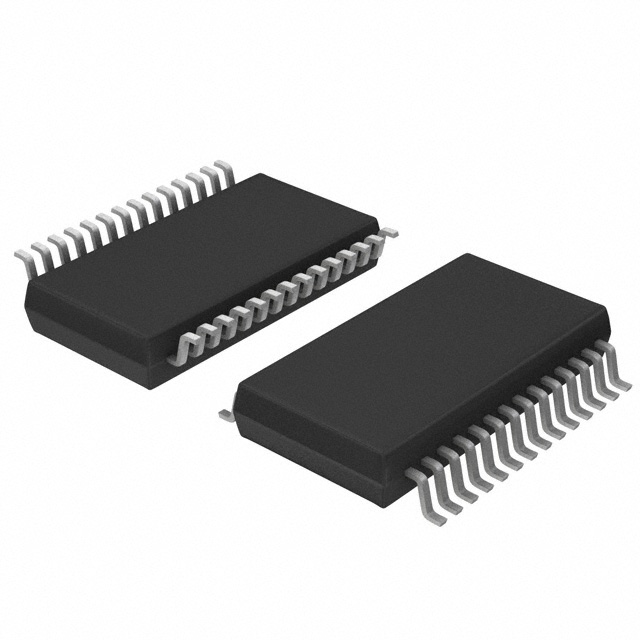
SP208E / SP211E / SP213E
Data Sheet
Low Power, High ESD +5V RS-232 Transceivers
General Description
Features
The SP208E-SP213E are enhanced transceivers intended
for use in RS-232 and V.28 serial communication. These
devices feature very low power consumption and singlesupply operation making them ideal for space-constrained
applications. MaxLinear on-board charge pump circuitry
generates fully compliant RS-232 voltage levels using small
and inexpensive 0.1µF charge pump capacitors. External
+12V and -12V supplies are not required. The SP211E and
SP213E feature a low-power shutdown mode, which reduces
power supply drain to 1µA. SP213E includes two receivers
that remain active during shutdown to monitor for signal
activity.
■
■
■
■
■
■
■
■
■
■
The SP208E-SP213E devices are pin-to-pin compatible with
our previous SP208, SP211 and SP213 as well as industrystandard competitor devices. Driver output and receiver
input pins are protected against ESD to over ±15kV for both
Human Body Model and IEC61000-4-2 Air Discharge test
methods. Data rates of 120kbps are guaranteed, making
them compatible with high speed modems and PC remoteaccess applications. Receivers also incorporate hysteresis
for clean reception of slow moving signals.
Meets all EIA-232 and ITU V.28 specifications
Single +5V supply operation
3mA typical static supply current
4 x 0.1μF external charge pump capacitors
120kbps transmission rates
Standard SOIC and SSOP footprints
1μA shutdown mode (SP211E & SP213E)
Two wake-up receivers (SP213E)
Tri-state / Rx enable (SP211E & SP213E)
Improved ESD specifications:
±15kV Human Body Model
±15kV IEC6100-4-2 Air Discharge
±8kV IEC6100-4-2 Contact Discharge
Table 1: Model Selection Table
Ordering Information - page 20
Device
Drivers
Receivers
Pins
SP208E
4
4
24
SP211E
4
5
28
SP213E
4
5
28
Typical Application
+5V INPUT
9
0.1μF
6.3V
10
0.1μF
6.3V
VCC
V+
12
13
0.1μF
16V
C1+
14
11
0.1μF
6.3V
C1–
C2+
V-
15
SP208E
0.1μF
16V
C2–
400kΩ
2
T1 OUT
18
T2
1
T2 OUT
400kΩ
T3 IN
19
T3
24
T3 OUT
400kΩ
R1 OUT
21
6
T4
20
7
R1
RS-232 OUTPUTS
T2 IN
T4 IN
TTL/CMOS OUTPUTS
RT1
400kΩ
T4 OUT
R1 IN
5kΩ
R2 OUT
4
3
R2
R2 IN
5kΩ
R3 OUT
22
23
R3
R3 IN
RS-232 INPUTS
TTL/CMOS INPUTS
T1 IN
5
5kΩ
R4 OUT
17
16
R4
R4 IN*
5kΩ
8
GND
Figure 1: SP208E Typical Application
• www.maxlinear.com• Rev 2.0.0
�SP208E / SP211E / SP213E Low Power, High ESD +5V RS-232 Transceivers Data Sheet
Revision History
Revision History
Document No.
Release Date
Change Description
-
01/27/06
Legacy Sipex Datasheet.
1.0.0
07/23/09
Convert to Exar format, update ordering information and change rev to 1.0.0
1.0.1
10/15/12
Change ESD ratings to IEC61000-4-2, remove typical 230kbps data rate reference and
update ordering information.
1.0.2
05/15/19
Update to MaxLinear format. Update ordering information. Removed obsolete SP207E. Added
ESD rating section after absolute maximums.
2.0.0
10/21/20
Update SP211E and SP213E output voltage swing, RS-232 input voltage range, ICC,
maximum storage temperature and absolute maximum RIN voltage. Update Transmitter /
Drivers and High Efficient Charge Pumps sections in the Description. Update Transmitter
Output graphs for SP211E and SP213E. Update Ordering Information.
Changes made in accordance to PCN 20014 (SP211E) and PCN 20015 (SP213E).
10/21/20
Rev 2.0.0
ii
�SP208E / SP211E / SP213E Low Power, High ESD +5V RS-232 Transceivers Data Sheet
Table of Contents
Table of Contents
General Description............................................................................................................................................. i
Features................................................................................................................................................................ i
Typical Application .............................................................................................................................................. i
Specifications ..................................................................................................................................................... 1
Absolute Maximum Ratings...........................................................................................................................................1
ESD Ratings ..................................................................................................................................................................1
Electrical Characteristics ...............................................................................................................................................2
Pin Information ................................................................................................................................................... 5
Pin Configurations .........................................................................................................................................................5
Description .......................................................................................................................................................... 6
Theory Of Operation......................................................................................................................................................6
Transmitter / Drivers.............................................................................................................................................6
Receivers .............................................................................................................................................................6
Highly Efficient Charge Pump ..............................................................................................................................6
Shutdown Mode ...................................................................................................................................................8
SP213E Wakeup Function ...................................................................................................................................8
Shutdown Conditions ...........................................................................................................................................8
Receiver Enable ...................................................................................................................................................9
ESD Tolerance ............................................................................................................................................................10
EIA Standards .............................................................................................................................................................12
Typical Application Circuits .........................................................................................................................................12
Mechanical Dimensions ................................................................................................................................... 15
SSOP24 ......................................................................................................................................................................15
Mechanical Dimensions ................................................................................................................................... 16
WSOIC24 ....................................................................................................................................................................16
Mechanical Dimensions ................................................................................................................................... 17
SSOP28 ......................................................................................................................................................................17
Recommended Land Pattern and Stencil....................................................................................................... 18
SSOP28 ......................................................................................................................................................................18
Mechanical Dimensions ................................................................................................................................... 19
WSOIC28 ....................................................................................................................................................................19
Ordering Information........................................................................................................................................ 20
10/21/20
Rev 2.0.0
iii
�SP208E / SP211E / SP213E Low Power, High ESD +5V RS-232 Transceivers Data Sheet
List of Figures
List of Figures
Figure 1: SP208E Typical Application ................................................................................................................... i
Figure 2: SP208E Transmitter Output @ 120kbps RL = 3kΩ, CL = 1000pF......................................................... 3
Figure 3: SP208E Transmitter Output @ 120kbps RL = 3kΩ, CL = 2500pF......................................................... 3
Figure 4: SP208E Transmitter Output @ 240kbps RL = 3kΩ, CL = 1000pF......................................................... 3
Figure 5: SP208E Transmitter Output @ 240kbps RL = 3kΩ, CL = 2500pF......................................................... 3
Figure 6: SP211E and SP213E Transmitter Output @ 120kbps RL = 3kΩ, CL = 1000pF.................................... 4
Figure 7: SP211E and SP213E Transmitter Output @ 120kbps RL = 3kΩ, CL = 2500pF.................................... 4
Figure 8: SP211E and SP213E Transmitter Output @ 240kbpsRL = 3kΩ, CL = 1000pF..................................... 4
Figure 9: SP211E and SP213E Transmitter Output @ 240kbps RL = 3kΩ, CL = 2500pF.................................... 4
Figure 10: SP208E Pin Configuration................................................................................................................... 5
Figure 11: SP211E Pin Configuration................................................................................................................... 5
Figure 12: SP213E Pin Configuration................................................................................................................... 5
Figure 13: Charge Pump - Phase 1 ...................................................................................................................... 7
Figure 14: Charge Pump - Phase 2 ...................................................................................................................... 7
Figure 15: Charge Pump - Phase 3 ...................................................................................................................... 7
Figure 16: Charge Pump - Phase 4 ...................................................................................................................... 7
Figure 17: Typical Waveforms Seen on Capacitor C2 When all Drivers are at Maximum Load .......................... 8
Figure 18: Wake-Up Timing.................................................................................................................................. 9
Figure 19: ESD Test Circuit for Human Body Model .......................................................................................... 10
Figure 20: ESD Test Circuit for IEC61000-4-2 ................................................................................................... 11
Figure 21: ESD Test Waveform for IEC61000-4-2 ............................................................................................. 11
Figure 22: Typical SP213E Application .............................................................................................................. 12
Figure 23: SP208E Typical Application .............................................................................................................. 13
Figure 24: SP211E Typical Application .............................................................................................................. 13
Figure 25: SP213E Typical Application .............................................................................................................. 14
Figure 26: Mechanical Dimension, SSOP24 ...................................................................................................... 15
Figure 27: Mechanical Dimensions, WSOIC24 .................................................................................................. 16
Figure 28: Mechanical Dimensions, SSOP28..................................................................................................... 17
Figure 29: Recommended Land Pattern and Stencil, SSOP28.......................................................................... 18
Figure 30: Mechanical Dimensions, WSOIC28 .................................................................................................. 19
10/21/20
Rev 2.0.0
iv
�SP208E / SP211E / SP213E Low Power, High ESD +5V RS-232 Transceivers Data Sheet
List of Tables
List of Tables
Table 1: Model Selection Table ............................................................................................................................. i
Table 2: Absolute Maximum Ratings .................................................................................................................... 1
Table 3: ESD Ratings ........................................................................................................................................... 1
Table 4: Electrical Characteristics ........................................................................................................................ 2
Table 5: Shutdown and Wake-Up Truth Tables.................................................................................................... 9
Table 6: Transceiver ESD Tolerance Levels ...................................................................................................... 12
Table 7: Ordering Information............................................................................................................................. 20
10/21/20
Rev 2.0.0
v
�SP208E / SP211E / SP213E Low Power, High ESD +5V RS-232 Transceivers Data Sheet
Specifications
Specifications
Absolute Maximum Ratings
Important: These are stress ratings only and functional operation of the device at these or any other above those indicated
in the operation sections of the specification below is not implied. Exposure to absolute maximum ratings conditions for
extended periods of time may affect reliability.
Table 2: Absolute Maximum Ratings
Parameter
Minimum
Maximum
Units
6.0
V
13.2
V
13.2
V
VCC +0.3
V
RIN, SP208E
±20
V
RIN, SP211E, SP213E
±25
V
V+, 0.3V
V-, –0.3V
V
-0.3
VCC + 0.3
V
VCC
VCC - 0.3
V+
VInput Voltages
TIN
-0.3
Output Voltages
TOUT
ROUT
Short Circuit Duration
Tout
Continuous
Power Dissipation per Package
24-pin SSOP (derate 11.2mW / oC above +70oC)
900
mW
24-pin SOIC (derate 12.5mW / oC above +70oC)
1000
mW
+70oC)
900
mW
28-pin SOIC (derate 12.7mW / oC above +70oC)
1000
mW
Limit
Units
HBM (Human Body Model), Driver Outputs and Receiver Inputs
±15
kV
IEC61000-4-2 Air Discharge, Driver Outputs and Receiver Inputs
±15
kV
IEC61000-4-2 Contact Discharge, Driver Outputs and Receiver Inputs
±8
kV
28-pin SSOP (derate 11.2mW /
oC
above
ESD Ratings
Table 3: ESD Ratings
Parameter
10/21/20
Rev 2.0.0
1
�SP208E / SP211E / SP213E Low Power, High ESD +5V RS-232 Transceivers Data Sheet
Electrical Characteristics
Electrical Characteristics
VCC at nominal ratings; 0.1µF charge pump capacitors; TMIN to TMAX, unless otherwise noted. Typical values are at VCC = 5V and
TA = 25°C
Table 4: Electrical Characteristics
Parameter
Test Condition
Minimum
Typical
Maximum
Units
0.8
V
TTL Inputs TIN, EN, SD
Logic threshold VIL
Logic threshold VIH
2.0
Logic pull-up current
TIN = 0V
Maximum transmission rate
CL = 1000pF, RL = 3kΩ
V
15
200
120
µA
kbps
TTL Outputs
Compatibility
TTL / CMOS
VOL
IOUT = 3.2mA, VCC = 5V
VOH
IOUT = -1.0mA
Leakage current
0V ≤ VOUT ≤ VCC; SP211E EN = 0V;
SP213E EN = VCC, TA = +25ºC
0.4
3.5
V
V
0.05
±10
µA
RS-232 Output
SP208E
All transmitter outputs loaded with
3kΩ to ground
±5
±7
V
SP211E, SP213E
All transmitter outputs loaded with
3kΩ to ground
±5
±8.7
V
Output resistance
VCC = 0V, VOUT = ±2V
300
Output short circuit current
Infinite Duration, VOUT = 0V
Output voltage swing
Ω
±25
mA
RS-232 Input
Voltage range
SP208E
SP211E, SP213E
TA = 25°C
Voltage threshold low
VCC = 5V, TA = 25°C
Voltage threshold high
VCC = 5V, TA = 25°C
Hysteresis
VCC = 5V
Resistance
VIN = ±15V, TA = 25°C
–15
15
V
–25
25
V
0.8
1.2
V
1.7
2.8
V
0.2
0.5
1.0
V
3
5
7
kΩ
1.5
µs
Dynamic Characteristics
Driver propagation delay
TTL to RS-232
1.5
Receiver propagation delay
RS-232 to TTL
0.5
µs
Instantaneous slew rate
CL = 50pF, RL = 3 - 7kΩ, TA = 25°C,
from ±3V
30
V/µs
Transition time
CL = 2500pF, RL = 3kΩ, measured
from -3V to +3V or +3V to -3V
1.5
µs
Output enable time
400
ns
Output disable time
250
ns
10/21/20
Rev 2.0.0
2
�SP208E / SP211E / SP213E Low Power, High ESD +5V RS-232 Transceivers Data Sheet
Electrical Characteristics
Table 4: Electrical Characteristics
Parameter
Test Condition
Minimum
Typical
Maximum
Units
4.50
5.00
5.50
V
3
6
mA
3
8
Power Requirements
VCC
ICC
ICC
SP208E
SP211E, SP213E
SP208E
SP211E, SP213E
Shutdown current
No load: VCC = ±10%, TA = 25°C
All transmitters RL = 3kΩ
TA = 25°C
15
mA
23
mA
1
10
µA
0
+70
ºC
-40
+85
ºC
-65
+150
ºC
Environmental and Mechanical
Operating Temperature
Commercial, _C
Extended, _E
Storage temperature
Package
_A
Shrink (SSOP) small outline
_T
Wide (SOIC) small outline
Figure 2: SP208E Transmitter Output @ 120kbps
RL = 3kΩ, CL = 1000pF
Figure 3: SP208E Transmitter Output @ 120kbps
RL = 3kΩ, CL = 2500pF
T
ittTransmitter
O t t @ 240kb
Figure 4: SP208E
Output @ 240kbps
RL = 3kΩ, CL = 1000pF
Figure 5: SP208E Transmitter Output @ 240kbps
RL = 3kΩ, CL = 2500pF
10/21/20
Rev 2.0.0
3
�SP208E / SP211E / SP213E Low Power, High ESD +5V RS-232 Transceivers Data Sheet
Electrical Characteristics
Figure 6: SP211E and SP213E Transmitter Output @
120kbps RL = 3kΩ, CL = 1000pF
Figure 7: SP211E and SP213E Transmitter Output @
120kbps RL = 3kΩ, CL = 2500pF
Figure 8: SP211E and SP213E Transmitter Output @
240kbpsRL = 3kΩ, CL = 1000pF
Figure 9: SP211E and SP213E Transmitter Output @
240kbps RL = 3kΩ, CL = 2500pF
10/21/20
Rev 2.0.0
4
�SP208E / SP211E / SP213E Low Power, High ESD +5V RS-232 Transceivers Data Sheet
Pin Information
Pin Information
Pin Configurations
SP208E
Figure 3: SP208E Pin Configuration
SP211E
Figure 4: SP211E Pin Configuration
SP213E
Figure 5: SP213E Pin Configuration
10/21/20
Rev 2.0.0
5
�SP208E / SP211E / SP213E Low Power, High ESD +5V RS-232 Transceivers Data Sheet
Description
Description
The SP208E, SP211E and SP213E multi–channel
transceivers fit most RS-232 / V.28 communication needs.
All of these devices feature low–power CMOS construction
and MaxLinear on-board charge pump circuitry to generate
RS-232 signal-voltages, making them ideal for applications
where +9V and -9V supplies are not available. The highly
efficient charge pump is optimized to use small and
inexpensive 0.1µF charge pump capacitors, saving board
space and reducing overall circuit cost.
Each device provides a different driver / receiver
combination to match standard application requirements.
SP208E is a 4-driver/4-receiver device, ideal for providing
handshaking signals in V.35 applications or other generalpurpose serial communications. The SP211E and SP213E
are each 3-driver, 5-receiver devices ideal for DTE serial
ports on a PC or other data-terminal equipment.
The SP211E and SP213E feature a low–power shutdown
mode, which reduces power supply drain to 1µA. The
SP213E includes a Wake-Up function which keeps two
receivers active in the shutdown mode, unless disabled by
the EN pin.
The family is available in 28 and 24 pin SO (wide) and
SSOP (shrink) small outline packages. Devices can be
specified for commercial (0˚C to +70˚C) and industrial/
extended (–40˚C to +85˚C) operating temperatures.
Theory Of Operation
MaxLinear RS-232 transceivers contain three basic circuit
blocks:
■
■
■
Transmitter / driver
Receiver
The drivers of the SP211E, and SP213E can be tri-stated
by using the SHUTDOWN function. In this “power-off”
state, the charge pump is turned off and VCC current drops
to 1µA typical. Driver output impedance will remain greater
than 300Ω, satisfying the RS-232 and V.28 specifications.
For SP211E, SHUTDOWN is active when pin 25 is driven
high. For SP213E, SHUTDOWN is active when pin 25 is
driven low.
Receivers
The receivers convert RS-232 level input signals to
inverted TTL level signals. Because signals are often
received from a transmission line where long cables and
system interference can degrade signal quality, the inputs
have enhanced sensitivity to detect weakened signals.
The receivers also feature a typical hysteresis margin of
500mV for clean reception of slowly transitioning signals in
noisy conditions. These enhancements ensure that the
receiver is virtually immune to noisy transmission lines.
Receiver input thresholds are between 1.2 to 1.7 volts
typical. This allows the receiver to detect standard TTL or
CMOS logic-level signals as well as RS-232 signals. If a
receiver input is left unconnected or un-driven, a 5kΩ
pulldown resistor to ground will commit the receiver to a
logic-1 output state.
Highly Efficient Charge Pump
Charge pump
The onboard dual-output charge pump is used to generate
positive and negative signal voltages for the RS-232
drivers. This enables fully compliant RS-232 and V.28
signals from a single power supply device.
SP211E and SP213E also include SHUTDOWN and
ENABLE functions.
Transmitter / Drivers
The drivers are single-ended inverting transmitters, which
accept either TTL or CMOS inputs and output the RS-232
signals with an inverted sense relative to the input logic
levels. Should the input of the driver be left open, an
internal pullup to VCC forces the input high, thus committing
the output to a logic-1 (MARK) state. The slew rate of the
transmitter output is internally limited to a maximum of
10/21/20
30V / µs in order to meet the EIA / RS-232 and ITU V.28
standards. The transition of the output from high to low
also meets the monotonicity requirements of the standard,
even when loaded. The transmitter outputs are protected
against infinite short-circuits to ground without degradation
in reliability.
The charge pumps use four external capacitors to hold and
transfer electrical charge. The MaxLinear design uses a
unique approach compared to older, less–efficient designs.
The pumps use a four–phase voltage shifting technique to
attain symmetrical V+ and V- power supplies.
Rev 2.0.0
6
�SP208E / SP211E / SP213E Low Power, High ESD +5V RS-232 Transceivers Data Sheet
Phase 1 - VSS Charge Store and Double
VCC = +5V
The positive terminals of capacitors C1 and C2 are charged
from VCC with their negative terminals initially connected to
ground. C1+ is then connected to ground and the stored
charge from C1- is superimposed onto C2-. Since C2+ is
still connected to VCC the voltage potential across C2 is
now 2 x VCC.
+
C1
–
–
–5V
+
–
–
–
+
VDD Storage Capacitor
VSS Storage Capacitor
C3
–5V
Figure 6: Charge Pump - Phase 1
+
VSS Storage Capacitor
C3
–5V
+7V
C1
+
–
C2
C4
+
–
–
+
+
–
VDD Storage Capacitor
VSS Storage Capacitor
C3
Figure 9: Charge Pump - Phase 4
VCC = +5V
The MaxLinear charge-pump generates V+ and Vindependently from VCC. Hence in a no–load condition V+
and V- will be symmetrical. Older charge pump
approaches generate V+ and then use part of that stored
charge to generate V-. Because of inherent losses, the
magnitude of V- will be smaller than V+ on these older
designs.
C4
C2
+
–
–
+
+
–
-7V
VDD Storage Capacitor
VSS Storage Capacitor
C3
Figure 7: Charge Pump - Phase 2
Phase 3 - VDD Charge Store and Double
Phase three is identical to the first phase. The positive
terminals of C1 and C2 are charged from VCC with their
negative terminals initially connected to ground. C1+ is then
connected to ground and the stored charge from C1- is
superimposed onto C2-. Since C2+ is still connected to VCC
the voltage potential across capacitor C2 is now 2 x VCC.
10/21/20
–
VCC = +5V
Phase two connects the negative terminal of C2 to the VSS
storage capacitor and the positive terminal of C2 to ground.
This transfers the doubled and inverted (V-) voltage onto
C3. Meanwhile, capacitor C1 is charged from VCC to
prepare it for its next phase.
–
–
VDD Storage Capacitor
The fourth phase connects the negative terminal of C2 to
ground and the positive terminal of C2 to the VDD storage
capacitor. This transfers the doubled (V+) voltage onto C4.
Meanwhile, capacitor C1 is charged from VCC to prepare it
for its next phase.
Phase 2 - VSS Transfer and Invert
+
–
+
Phase 4 - VDD Transfer
C4
+
C2
–5V
C1
C2
+
Figure 8: Charge Pump - Phase 3
+5V
+
C4
+5V
VCC = +5V
C1
Description
The clock rate for the charge pump typically operates at
greater than 15kHz, allowing the pump to run efficiently
with small 0.1µF capacitors. Efficient operation depends
on rapidly charging and discharging C1 and C2, therefore
capacitors should be mounted close to the IC and have low
ESR (equivalent series resistance). Low cost surface
mount ceramic capacitors (such as are widely used for
power-supply decoupling) are ideal for use on the charge
pump.
However the charge pumps are designed to be able to
function properly with a wide range of capacitor styles and
values. If polarized capacitors are used, the positive and
negative terminals should be connected as shown.
Rev 2.0.0
7
�SP208E / SP211E / SP213E Low Power, High ESD +5V RS-232 Transceivers Data Sheet
Voltage potential across any of the capacitors will never
exceed 2 x VCC. Therefore capacitors with working
voltages as low as 10V rating may be used with a nominal
VCC supply. C1 will never see a potential greater than
VCC, so a working voltage of 6.3V is adequate. The
reference terminal of the VDD capacitor may be connected
either to VCC or ground, but if connected to ground a
minimum 16V working voltage is required. Higher working
voltages and / or capacitance values may be advised if
operating at higher VCC or to provide greater stability as the
capacitors age.
+7V
a) C2+
GND
GND
b) C2–
Description
SP213E Wakeup Function
On the SP213E, shutdown will tri-state receivers 1 - 3.
Receivers 4 and 5 remain active to provide a “wake-up”
function and may be used to monitor handshaking and
control inputs for activity. With only two receivers active
during shutdown, the SP213E draws only 5 - 10µA of
supply current.
Many standard UART devices may be configured to
generate an interrupt signal based on changes to the Ring
Indicate (RI) or other inputs. A typical application of this
function would be to detect modem activity with the
computer in a power–down mode. The ring indicator signal
from the modem could be passed through an active
receiver in the SP213E that is itself in the shutdown mode.
The ring indicator signal would propagate through the
SP213E to the power management circuitry of the
computer to power up the microprocessor and the SP213E
drivers. After the supply voltage to the SP213E reaches
+5.0V, the SHUTDOWN pin can be disabled, taking the
SP213E out of the shutdown mode.
All receivers that are active during shutdown maintain
500mV (typ.) of hysteresis. All receivers on the SP213E
may be put into tri-state using the ENABLE pin.
–7V
Figure 10: Typical Waveforms Seen on Capacitor C2
When all Drivers are at Maximum Load
Shutdown Conditions
For complete shutdown to occur and the 10µA power drain
to be realized, the following conditions must be met:
Shutdown Mode
SP211E and SP213E feature a control input which will shut
down the device and reduce the power supply current to
less than 10µA, making the parts ideal for battery-powered
systems. In shutdown mode the transmitters will be tristated, the V+ output of the charge pump will discharge to
VCC and the V- output will discharge to ground. Shutdown
will tri-state all receiver outputs of the SP211E.
SP211E:
■
■
+5V must be applied to the SD pin
■
The transmitter inputs must be either +5.0V or not
connected
■
■
ENABLE must be either Ground, +5.0V or not
connected
VCC must be +5V
Receiver inputs must be >0V and 0V and


 工商网监
湘ICP备2023018690号
工商网监
湘ICP备2023018690号
