SP337E
3.3V TO 5V RS-232/RS-485/RS-422 MULTIPROTOCOL TRANSCEIVER
July 5, 2021
Rev . 2.0.0
GENERAL DESCRIPTION
FEATURES
The SP337E is a dual mode serial transceiver
containing both RS-232 and RS-485/422 line drivers
and receivers. The RS-232 mode provides three
drivers and five receivers to support all eight signals
commonly used in the DB9 serial port connector
(3TX/5RX). In RS-485 mode the device features two
independent high speed RS-485/422 transmit and
receive channels (2TX/2RX). The default RS-485
configuration is full-duplex, but half-duplex operation
can be obtained by tying together the TX and RI pins,
and the TXEN and RXEN signals.
• 3.3V to 5V Single Supply Operation
• Robust ±15kV ESD Protection
Human Body Model
• Max Data Rate of 15Mbps in RS-485 mode
and up to 1Mbps in RS-232 mode (SP337EU)
• 3 Drivers, 5 Receivers RS-232/V.28
• 2 Drivers, 2 Receivers RS-485/RS-422
The SP337E is pin compatible to MaxLinear’s SP334.
Full-Duplex Configuration
1/8th Unit Load, up to 256 receivers on bus
• RS-485 Advanced Failsafe on Open, Short or
The SP337EB features a maximum data rate of
250kbps in RS-232 mode and a maximum data rat e
of 15Mbps in RS-485. However, the SP337EU
features a maximum data rate of 1Mbps in RS-232
mode and a maximum data rate of 15Mbps in RS-485
mode.
Terminated Lines
• Full Differential Driver Tri-State (Hi-Z) Control
• Receiver Output Tri-State Control
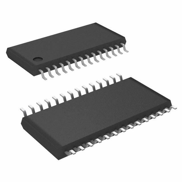
• TSSOP-28 Package
The MaxLinear-patented high efficiency charge
pumps (5,306,954) deliver true RS-232 driver out put
voltages from a single power supply from 3.3V to 5V.
Charge pump outputs are self-monitored to minimize
power consumption. The SP337E requires only four
0.1µF capacitors for complete functionality.
TYPICAL APPLICATIONS
•
•
•
•
•
•
•
All RS-485 receivers or transceivers feature high
impedance inputs which allow up to 256 transceivers
on a single shared bus. When configured in RS -485
mode, each driver may be individually enabled or put
into tri-state, simplifying use on shared bus es or for
bidirectional communication. The RS-485/422 drivers
can be disabled (high-Z output) by the TXEN enable
pin. The RS-232 receiver outputs can be disabled by
the RXEN enable pin.
All receivers have advanced failsafe protection to
prevent oscillation when inputs are un-connected. In
RS-232 mode, each receiver input has a 5kΩ pulldown to ground. in RS-485 mode, receivers will
default to output logic 1 if inputs are floating, shorted,
or open but terminated.
All driver outputs and receiver inputs are protected
against ESD strikes up to ±15,000 volts.
1
Dual Protocol Serial Ports (RS-232 or RS-485)
Industrial Computers
Industrial and Process Control Equipment
Point-Of-Sales Equipment
Networking Equipment
HVAC Controls Equipment
Building Security Equipment
�SP337E
3.3V TO 5V RS-232/RS-485/RS-422 MULTIPROTOCOL TRANSCEIVER
FIGURE 1. TYPICAL RS-232 AND RS-485 APPLICATION CIRCUITS
ORDERING INFORMATION
PART NUMBER
OPERATING TEMPERATURE RANGE
PACKAGE
PACKAGING M ETHOD
LEAD -FREE
SP337EBEY-L
-40°C to +85°C
28-pin TSSOP
Tube
Yes
SP337EBEY-L/TR
-40°C to +85°C
28-pin TSSOP
Tape and Reel
Yes
SP337EUEY-L
-40°C to +85°C
28-pin TSSOP
Tube
Yes
SP337EUEY-L/TR
-40°C to +85°C
28-pin TSSOP
Tape and Reel
Yes
XR21B1420IL28-0A-EVB
The XR21B1420 Evaluation Board includes the SP339E transceiver.
NOTE: For the most up-to-date ordering information and additional information on environmental rating, go to
w ww.maxlinear.com/SP337.
208DSR00
2
Rev. 2.0.0
�SP337E
3.3V TO 5V RS-232/RS-485/RS-422 MULTIPROTOCOL TRANSCEIVER
PIN DESCRIPTIONS
Pin Assignments
PIN #
1
PIN NAME
TI3
DESCRIPTION
TYPE
Input
RS-232
RS-485/RS-422
T3 Driver TTL input
T3 Driver TTL input
This pin has a 400k pull-up to Vcc in both RS-232 and RS-485 modes.
The pull-up is disabled in the SP337EU shutdow n mode.
X*
Only RS-485 mode
2
TXEN
Input
3
TX4
Output
X*
T3(Z) Inverting Output
4
TX3
Output
T3 Driver Output
T3(Y) Non-Inverting Output
5
Vcc
Pow er
6
TX1
Output
T1 Driver Output
T1(Y) Non-Inverting Output
7
TX2
Output
T2 Driver Output
T1(Z) Inverting Output
8
GND
Pow er
Ground
9
C1+
Pump
Positive Terminal of Positive Flying Capacitor
10
V+
Pump
Vdd Storage Capacitor
11
C2+
Pump
Positive Terminal of Negative Flying Capacitor
12
C1-
Pump
Negative Terminal of Positive Flying Capacitor
13
C2-
Pump
Negative Terminal of Negative Flying Capacitor
14
V-
Pump
Vss Storage Capacitor
15
RI1
Input
R1 Receiver Input, 5k pull-dow n
R1(B) Receiver Inverting Input
16
RI2
Input
R2 Receiver Input, 5k pull-dow n
R1(A) Receiver Non-Inverting Input
17
RI3
Input
R3 Receiver Input, 5k pull-dow n
R3(A) Receiver Non-Inverting Input
18
RI4
Input
R4 Receiver Input, 5k pull-dow n
R3(B) Receiver Inverting Input
19
RX1
Output
20
RX2
Output
21
RX3
Output
22
RX4
Output
R4 Receiver Output
X*
23
RX5
Output
R5 Receiver Output
X*
24
RI5
Input
R5 Receiver Input, 5k pull-dow n
X*
25
RS232/RS485
Input
Mode select, either RS-232 (low ) or RS-485/422 (high) mode
26
RXEN
Input
Receiver enable for both RS-232 and RS-485/422 mode (Active low )
208DSR00
This pin has a 400k pull-up to Vcc in both RS-232 and RS-485 modes.
The pull-up is disabled in the SP337EU shutdow n mode.
Pow er Supply Voltage, betw een 3.3V and 5V
R1 Receiver Output
R2 Receiver Output
X*
R3 Receiver Output
3
Rev. 2.0.0
�SP337E
3.3V TO 5V RS-232/RS-485/RS-422 MULTIPROTOCOL TRANSCEIVER
Pin Assignments
PIN #
27
PIN NAME
TI1
TYPE
Input
DESCRIPTION
RS-232
RS-485/RS-422
T1 Driver Input
T1 Driver Input
This pin has a 400k pull-up to Vcc in both RS-232 and RS-485 modes.
The pull-up is disabled in the SP337EU shutdow n mode.
T2 Driver Input
28
TI2
Input
X*
This pin has a 400k pull-up to Vcc in both RS-232 and RS-485 modes.
The pull-up is disabled in the SP337EU shutdow n mode.
*
Pins marked with an X in the above table are ignored or "don’t care" in the listed mode, provided
they do not exceed VCC or go below ground. Some of these pins have a pull-up to VCC which
remains active in both RS-232 and RS-485 mode, but is disabled in the SP337EU shutdown mode.
208DSR00
4
Rev. 2.0.0
�SP337E
3.3V TO 5V RS-232/RS-485/RS-422 MULTIPROTOCOL TRANSCEIVER
ABSOLUTE MAXIMUM RATINGS
These are stress ratings only and functional operation of the device at these ratings or any other above those indicated in the ope r a ti o n s e cti o n s t o t h e
specif ications below is not implied. Exposure to absolute maximum rating conditions for extended periods of time may affect reliability and cause permanen t
damage to the device.
Supply Voltage V CC
+6.0V
Receiver Input V IN (DC Input Voltage)
-16V to +16V
Input Voltage at TTL input Pins
-0.3V to Vcc + 0.5V
Driver Output Voltage (from Ground)
-7.5V to +12.5V
Short Circuit Duration, TXout to GND
Continuous
Storage Temperature Range
-65°C to + 150°C
Lead Temperature (soldering, 10s)
+300°C
Pow er Dissipation 28-pin TSSOP
(derate 12mW/°C above +70°C)
657mW
ESD Ratings
HBM - Human Body Model (TX and RI Pins 3, 4, 6, 7, 15, 16, 17, 18, 24)
±15kV
HBM - Human Body Model (all other pins)
± 2kV
IEC 61000-4-2 Airgap Discharge (TX & RI Pins)
±15kV
IEC 61000-4-2 Contact Discharge (TX & RI Pins)
± 8kV
CAUTION:
ESD (Electrostatic Discharge) sensitive device. Permanent damage may occur on unconnected devices subject to high energy electrostatic fields. Un u s ed
dev ices must be stored in conductive foam or shunts. Personnel should be properly grounded prior to handling this device. The protective foam should be
discharged to the destination socket before devices are removed.
ELECTRICAL CHARACTERISTICS
UNLESS OTHERW ISE NOTED: V CC = +3.3V
±5% OR +5.0V ±5%, C1-C4
= 0.1µ F; TA = TMIN TO TMAX.
TYPICAL VALUES ARE AT V CC = 3.3V, TA = +25 O C.
SYMBOL
PARAMETERS
M IN .
TYP.
M AX.
UNITS
CONDITIONS
DC CHARACTERISTICS
ICC
Supply Current (RS-232)
1.5
6.0
mA
No Load, RS232/RS485 = 0V
ICC
Supply Current (RS-485)
7.0
15
mA
No Load, RS232/RS485 = V CC
ICC
Vcc Shutdow n Current
(SP337EU only)
1.0
10.0
µA
TXEN = 0V, RXEN = V CC
(SP337EU only)
TRANSMITTER and LOGIC INPUT PINS: Pins 1, 2, 25, 26, 27, 28
V IH
Logic Input Voltage HIGH
2.0
V
V CC = 3.3V
V IH
Logic Input Voltage HIGH
2.4
V
V CC = 5.0V
V IL
Logic Input Voltage LOW
0.8
V
IIL
Logic Input Leakage Current
1.0
µA
Input High (V IN = V CC)
IPU
Logic Input Pull-up Current
15.0
µA
Input Low (V IN = 0V)
V HY S
208DSR00
Logic Input Hysteresis
0.5
5
V
Rev. 2.0.0
�SP337E
3.3V TO 5V RS-232/RS-485/RS-422 MULTIPROTOCOL TRANSCEIVER
UNLESS OTHERW ISE NOTED: V CC = +3.3V
±5% OR +5.0V ±5%, C1-C4
= 0.1µ F; TA = TMIN TO
TMAX. TYPICAL VALUES ARE AT V CC = 3.3V, TA = +25 C.
O
SYMBOL
PARAMETERS
M IN .
TYP.
M AX.
UNITS
CONDITIONS
RS-232 and RS-485/422 RECEIVER OUTPUTS: Pins 19, 20, 21, 22, 23
V OH
Receiver Output Voltage HIGH
V OL
Receiver Output Voltage LOW
IOSS
Receiver Output ShortCircuit Current
IOZ
Receiver Output Leakage Current
V
IOUT = 1.0mA
0.4
V
IOUT = -3.2mA
±40
±65
mA
0 < V O < V CC
±0.1
±1.5
µA
Receivers Disabled
+15
V
VCC-0.6
SINGLE-ENDED RECEIV ER INPUTS (RS-232)
Input Voltage Range
-15
Input Threshold Low
0.6
1.2
V
V CC = 3.3V
0.8
1.5
V
V CC = 5.0V
Input Threshold HIGH
Input Hysteresis
1.5
2.0
V
V CC = 3.3V
1.8
2.4
V
V CC = 5.0V
0.5
Input Resistance
3
5
V
7
kΩ
DIFFERENTIAL RECEIV ER INPUTS (RS-485 / RS-422)
RIN
Receiver Input Resistance
V TH
Receiver Differential Threshold
∆V TH
IIN
kΩ
96
-200
Receiver Input Hysteresis
-125
-50
mV
mV
V CM = 0V
125
µA
V IN = 12V
-100
µA
V IN = -7V
30
Input Current
-7V ≤ V CM ≤ + 12V
SINGLE-ENDED DRIVER OUTPUTS (RS-232)
VO
±5.0
Output Voltage Sw ing
±5.4
Short Circuit Current
Pow er Off Impedance
300
V
Output Loaded w ith 3kΩ to Gnd
±7.0
V
No Load Output
±60
mA
V O = 0V
Ω
V CC = 0V; V O = ±2V
10M
DIFFERENTIAL DRIVER OUTPUTS (RS-485 / RS-422)
V OD
∆V OD
V OC
∆V OC
208DSR00
Differential Driver Output (Tx_Out)
Change In Magnitude of
Differential Output Voltage
Driver CommonMode Output Voltage
Change In Magnitude of
Common Mode Output Voltage
6
2
V CC
V
RL = 100Ω (RS-422), Figure 2
1.5
V CC
V
RL = 54Ω (RS-485), Figure 2
1.5
V CC
V
V CM = -7V, Figure 3
1.5
V CC
V
V CM = +12V, Figure 3
-0.2
+0.2
V
RL = 54Ω or 100Ω , Figure 2
3
V
RL = 54Ω or 100Ω , Figure 2
0.2
V
RL = 54Ω or 100Ω , Figure 2
Rev. 2.0.0
�SP337E
3.3V TO 5V RS-232/RS-485/RS-422 MULTIPROTOCOL TRANSCEIVER
UNLESS OTHERW ISE NOTED: V CC = +3.3V
±5% OR +5.0V ±5%, C1-C4
= 0.1µ F; TA = TMIN TO TMAX.
TYPICAL VALUES ARE AT V CC = 3.3V, TA = +25 C.
O
SYMBOL
IOSD
IO
PARAMETERS
M IN .
TYP.
Driver Output Short Circuit Current
Output Leakage Current
M AX.
UNITS
CONDITIONS
±250
mA
V = +12V to -7V, Figure 4
±100
µA
TXEN = 0V or Shutdow n,
V O = +12V to -7V, Vcc = 0V or
5.25V
TIMING CHARACTERISTICS
RS-232 (SP337EB ONLY) DATA RATE = 250kbps, ONE TRANSMITTER SWITCHING
Maximum Data Rate
tPHL, tPLH
tPHL-tPLH
tPHL, tPLH
tPHL-tPLH
tTHL, tTLH
250
Receiver Propagation Delay
kbps
100
Receiver Skew
100
Driver Propagation Delay
800
ns
CL = 150pF, Figures 20 and 21
ns
CL = 150pF, Figures 20 and 21
ns
Driver Skew
400
ns
Receiver Output Enable time
400
ns
Receiver Output Disable time
400
ns
30
V/µs
Transition-Region Slew Rate from
+3.0V to -3.0V or -3.0V to +3.0V
4
RL = 3kΩ, CL = 1000pF
V CC = 3.3V, RL = 3kΩ to 7kΩ,
CL = 150pF to 2500pF,
Figures 18 and 19
RS-232 (SP337EU ONLY) DATA RATE = 1Mbps, ONE TRANSMITTER SWITCHING
Maximum Data Rate
tPHL, tPLH
tPHL-tPLH
tPHL, tPLH
tPHL-tPLH
tTHL, tTLH
1
Receiver Propagation Delay
Mbps
100
100
Receiver Skew
Driver Propagation Delay
250
ns
CL = 150pF, Figures 20 and 21
ns
CL = 150pF, Figures 20 and 21
ns
Driver Skew
150
ns
Receiver Output Enable time
400
ns
Receiver Output Disable time
400
ns
Transition-Region Slew Rate from
+3.0V to -3.0V or -3.0V to +3.0V
RL = 3kΩ, CL = 250pF
V/µs
50
V CC = 3.3V, RL = 3kΩ,
CL = 150pF, Figures 18 and 19
RS-485/RS-422 (SP337EB and SP337EU) DATA RATE = 15Mbps, ONE TRANSMITTER SWITCHING
Maximum Data Rate
15
20
Mbps
RDIFF = 54Ω, CL = 50pF
Differential Output Propagation
Delay Time
60
120
ns
Figures 5 and 6
Driver Rise and Fall Time
15
25
ns
Figures 5 and 6
Driver Propagation Delay Skew
10
ns
Figures 5 and 6
tDZH , tDZL
Driver Output Enable Time
400
ns
Figures 7, 8, 9 and 10
tDHZ , tDLZ
Driver Output Disable Time
400
ns
Figures 7, 8, 9 and 10
tPHL, tPLH
Receiver Propagation Delay
150
ns
Figures 11 and 12
tDPHL, tDPLH
tR, tF
tDPHLtDPLH
208DSR00
80
7
Rev. 2.0.0
�SP337E
3.3V TO 5V RS-232/RS-485/RS-422 MULTIPROTOCOL TRANSCEIVER
UNLESS OTHERW ISE NOTED: V CC = +3.3V
±5% OR +5.0V ±5%, C1-C4
= 0.1µ F; TA = TMIN TO
TMAX. TYPICAL VALUES ARE AT V CC = 3.3V, TA = +25 C.
O
SYMBOL
PARAMETERS
M IN .
TYP.
M AX.
UNITS
CONDITIONS
tZH
Receiver Enable to Output High
100
200
ns
Figures 13 and 14
tZL
Receiver Enable to Output Low
100
200
ns
Figures 13 and 15
tHZ
Receiver Output High to Disable
100
200
ns
Figures 13 and 16
tLZ
Receiver Output Low to Disable
100
200
ns
Figures 13 and 17
RS-485/RS-422 SHUTDOWN FEATURE APPLIES TO SP337EU ONLY
tDZZV
tDshutdw
n
tRZZV
tRshutdw
n
Shutdow n to Driver Output Valid
30
Driver Time to Shutdow n
100
Shutdow n to Receiver Output Valid
ns
30
Receiver Time to Shutdow n
µs
100
µs
ns
FIGURE 2. RS-485 DRIVER DC TEST CIRCUIT
RL/2
DI
VOD
T
RL/2 VOC
VCC
FIGURE 3. RS-485 DRIVER COMMON MODE LOAD TEST
DE = 3.3V
DI = 0 or Vcc
375Ω
A
Tx
VOD
B
208DSR00
60Ω
375Ω
8
VCM
Rev. 2.0.0
�SP337E
3.3V TO 5V RS-232/RS-485/RS-422 MULTIPROTOCOL TRANSCEIVER
FIGURE 4. RS-485 DRIVER OUTPUT SHORT CIRCUIT TEST
FIGURE 5. RS-485 DRIVER PROPAGATION DELAY TEST CIRCUIT
DI
A
Tx
VOD
RL
54Ω
CL
50pF
B
3.3V
FIGURE 6. RS-485 DRIVER TIMING DIAGRAM
208DSR00
9
Rev. 2.0.0
�SP337E
3.3V TO 5V RS-232/RS-485/RS-422 MULTIPROTOCOL TRANSCEIVER
FIGURE 7. RS-485 DRIVER ENABLE
AND DISABLE
TEST CIRCUI
FIGURE 8. RS-485 DRIVER ENABLE
AND DISABLE
TIMING DIAGRAM
FIGURE 9. RS-485 DRIVER ENABLE
AND DISABLE
TEST CIRCUIT 2
208DSR00
10
Rev. 2.0.0
�SP337E
3.3V TO 5V RS-232/RS-485/RS-422 MULTIPROTOCOL TRANSCEIVER
FIGURE 10. RS-485 DRIVER ENABLE
AND DISABLE
TIMING DIAGRAM 2
FIGURE 11. RS-485 RECEIVER PROPAGATION DELAY TEST CIRCUIT
FIGURE 12. RS-485 RECEIVER PROPAGATION DELAY TIMING DIAGRAM
208DSR00
11
Rev. 2.0.0
�SP337E
3.3V TO 5V RS-232/RS-485/RS-422 MULTIPROTOCOL TRANSCEIVER
FIGURE 13. RS-485 RECEIVER ENABLE AND DISABLE TIMES TEST CIRCUIT
OUT
1.5V
S3
-1.5V
A
B
Vcc
1kΩ
R
S2
RE
GENERATOR
S1
CL= 15pF
50Ω
FIGURE 14. RS-485 RECEIVER ENABLE AND DISABLE TIMES TIMING DIAGRAM 1
FIGURE 15. RS-485 RECEIVER ENABLE AND DISABLE TIMES TIMING DIAGRAM 2
208DSR00
12
Rev. 2.0.0
�SP337E
3.3V TO 5V RS-232/RS-485/RS-422 MULTIPROTOCOL TRANSCEIVER
FIGURE 16. RS-485 RECEIVER ENABLE AND DISABLE TIMES TIMING DIAGRAM 3
FIGURE 17. RS-485 RECEIVER ENABLE AND DISABLE TIMES TIMING DIAGRAM 4
FIGURE 18. RS-232 DRIVER OUTPUT SLEW RATE TEST CIRCUIT
Tx
GENERATOR
208DSR00
50Ω
13
OUT
CL
RL
Rev. 2.0.0
�SP337E
3.3V TO 5V RS-232/RS-485/RS-422 MULTIPROTOCOL TRANSCEIVER
FIGURE 19. RS-232 DRIVER OUTPUT SLEW RATE TIMING DIAGRAM
Input
3V
1.5V
0
+3V
OUT
V OL
-3V
tTHL
tTLH
FIGURE 20. RS-232 RECEIVER PROPAGATION DELAY TESTCIRCUIT
Rx
GENERATOR
OUT
CL
50Ω
FIGURE 21. RS-232 RECEIVER PROPAGATION DELAY TIMING DIAGRAM
Input
1.5V
+3V
1.5V
-3V
tPLH
tPHL
VOH
OUT
50%
50%
VOL
208DSR00
14
Rev. 2.0.0
�SP337E
3.3V TO 5V RS-232/RS-485/RS-422 MULTIPROTOCOL TRANSCEIVER
SP337E Mode Configuration Tables
TABLE 1: SP337EB
Operation
RS232/RS485
TXEN
RXEN
Charge Pump
Driver and Receiver
Low
Ignored
Low
RS-232
3T/5R
ON
Receivers Enabled
Low
Ignored
High
RS-232
3T/5R
ON
Receivers Disabled
(High-Z Output)
High
Low
Low
RS-485/422
Full-Duplex
2T/2R
ON
Drivers Disabled
(High-Z Output);
Receivers Enabled
High
High
High
RS-485/422
Full-Duplex
2T/2R
ON
Drivers Enabled;
Receivers Disabled
(High-Z Output)
High
Low
High
RS-485/422
Full-Duplex
2T/2R
ON
Drivers Disabled
(High Z output);
Receivers Disabled
(High Z output)
High
High
Low
RS-485/422
Full-Duplex
2T/2R
ON
Drivers Enabled;
Receivers Enabled
Charge Pump
Driver and Receiver
TABLE 2: SP337EU
Operation
RS232/RS485
TXEN
RXEN
Low
Ignored
Low
RS-232
3T/5R
ON
Receivers Enabled
Low
Ignored
High
RS-232
3T/5R
ON
Receivers Disabled
(High-Z Output)
High
Low
Low
RS-485/422
Full-Duplex
2T/2R
ON
Drivers Disabled
(High-Z Output);
Receivers Enabled
High
High
High
RS-485/422
Full-Duplex
2T/2R
ON
Drivers Enabled;
Receivers Disabled
(High-Z Output)
High
Low
High
RS-485/422
Full-Duplex
2T/2R
OFF
(Shutdown)
Drivers Disabled
(High Z output);
Receivers Disabled
(High Z output)
High
High
Low
RS-485/422
Full-Duplex
2T/2R
ON
Drivers Enabled;
Receivers Enabled
208DSR00
15
Rev. 2.0.0
�SP337E
3.3V TO 5V RS-232/RS-485/RS-422 MULTIPROTOCOL TRANSCEIVER
FIGURE 22. 28 PIN TSSOP PACKAGE OUTLINE DRAWING
TOP VIEW
SIDE VIEW 1
SIDE VIEW 2
©
©
DETAIL A
©
©
TERMI N A L DETAILS
Drawing No.: POD-000000 134
Revision: A
208DSR00
16
Rev. 2.0.0
�SP337E
3.3V TO 5V RS-232/RS-485/RS-422 MULTIPROTOCOL TRANSCEIVER
FIGURE 23. 28 PIN TSSOP RECOMMENDED LAND PATTERN AND STENCIL
TYPICAL RECOM M E N DE D
LAND PATTE RN
TYPICAL RECOM M E N DE D
STENCI L
Drawing No.: POD-000000 134
Revision: A
208DSR00
17
Rev. 2.0.0
�SP337E
3.3V TO 5V RS-232/RS-485/RS-422 MULTIPROTOCOL TRANSCEIVER
REVISION HISTORY
DATE
REVISION
DESCRIPTION
December 2010
1.0.0
Production Release.
December 2010
1.0.1
Update ESD Information.
March 2011
1.0.2
Correct Figure 1 RS-485 driver type error.
March 2018
1.0.3
Clarify test conditions for Driver Output Leakage Current on page 7. Corrected
pow er off impedance unit. Update to MaxLinear logo. Update format and Ordering
Information. Moved ESD ratings / protection to Absolute Maximum Ratings section.
July 5, 2021
2.0.0
Add missing units for RS-232 driver propagation delays and ESD protection ratings
for IEC61000-4-2. Update SP337EB 250kbps conditions, and RS-485 / RS-422
shutdow n to driver / receiver output valid timing according to the changes outlined
in PCN 20006. Update ordering information and remove obsolete WSOIC version
references.
Corporate Headquarters:
5966 La Place Court
Suite 100
Carlsbad, CA 92008
Tel.: +1 (760) 692-0711
Fax: +1 (760) 444-8598
www.maxlinear.com
The content of this document is furnished for informational use only, is subject to change without notice, and should not be construed as a commitment by MaxLinear, Inc. MaxLinear, Inc.
assumes no responsibility or liability for any errors or inaccuracies that may appear in the informational content contained in this guide. Complying with all applicable copyright laws is the
responsibility of the user. Without limiting the rights under copyright, no part of this document may be reproduced into, stored in, or introduced into a retrieval system, or transmitted in any
form or by any means (electronic, mechanical, photocopying, recording, or otherwise), or for any purpose, without the express written permission of MaxLinear, Inc.
MaxLinear, Inc. does not recommend the use of any of its products in life support applications where the failure or malfunction of the product can reasonably be expected to cause failure of
the life support system or to significantly affect its safety or effectiveness. Products are not authorized for use in such applications unless MaxLinear, Inc. receives, in writing, assurances to
its satisfaction that: (a) the risk of injury or damage has been minimized; (b) the user assumes all such risks; (c) potential liability of MaxLinear, Inc. is adequately protected under the
circumstances.
MaxLinear, Inc. may have patents, patent applications, trademarks, copyrights, or other intellectual property rights covering subject matter in this document. Except as expressly provided in
any written license agreement from MaxLinear, Inc., the furnishing of this document does not give you any license to these patents, trademarks, copyrights, or other intellectual property.
MaxLinear, the MaxLinear logo, any MaxLinear trademarks (MxL, Full-Spectrum Capture, FSC, G.now, AirPHY, Puma, and AnyWAN), and the MaxLinear logo on the products sold are all
property of MaxLinear, Inc. or one of MaxLinear’s subsidiaries in the U.S.A. and other countries. All rights reserved. *Other company trademarks and product names appearing herein are
the property of their respective owners.
© 2021 MaxLinear, Inc. All rights reserved.
208DSR00
18
Rev. 2.0.0
�


 工商网监
湘ICP备2023018690号
工商网监
湘ICP备2023018690号

