DATA SHEET
AAT1110: Fast Transient 800 mA Step-Down Converter
Applications
Description
Cellular phones
The AAT1110 SwitchReg™ is a member of Skyworks' Total
Power Management IC (TPMIC™) product family. It is a 1.4 MHz
step-down converter with an input voltage range of 2.7 V to 5.5 V
and output as low as 0.6 V. Its low supply current, small size, and
high switching frequency make the AAT1110 the ideal choice for
portable applications.
Digital cameras
Handheld instruments
Microprocessor/DSP core/IO power
PDAs and handheld computers
The AAT1110 is available in either a fixed version with internal
feedback or a adjustable version with external feedback resistors.
It can deliver up to 800 mA of load current while maintaining a
low 27 A no-load quiescent current. The 1.4 MHz switching
frequency minimizes the size of external components while
keeping switching losses low. The AAT1110 has excellent load
regulation and transient response with a small output inductor
and capacitor.
USB devices
Features
VIN range: 2.7 V to 5.5 V
VOUT fixed or adjustable from 0.6 V to VIN
27 A no-load quiescent current
Output current up to 800 mA
The AAT1110 is designed to maintain high efficiency throughout
the operating range and provides fast turn-on time.
1.4 MHz switching frequency
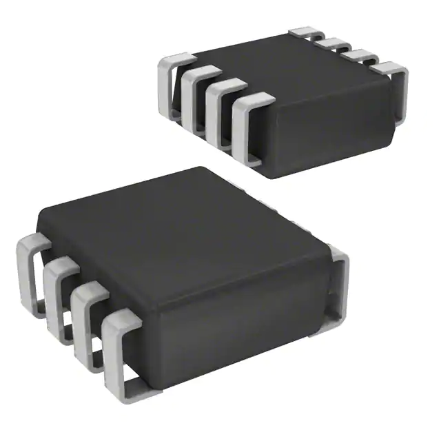
The AAT1110 is available in a space-saving 2.0 mm 2.2 mm
SC70JW-8 package and is rated over the 40 °C to +85 °C
temperature range.
120 s soft start
Fast load transient
Over-temperature protection
A typical application circuit is shown in Figure 1. The pin
configuration is shown in Figure 2. Signal pin assignments and
functional pin descriptions are provided in Table 1.
Current limit protection
100% duty cycle low-dropout operation
Shutdown current: 0.6 V output
0.1
%/V
0.2
250
A
k
s
Soft-start time
tSS
From enable to output regulation
Oscillator frequency
fOSC
TA = 25 °C
120
Over-temperature shutdown threshold
TSD
140
°C
Over-temperature shutdown hysteresis
THYS
15
°C
1.0
1.4
2.0
MHz
EN
Enable threshold low
VEN(L)
Enable threshold high
VEN(H)
Input low current
IEN
0.6
1.4
VIN = VOUT = 5.5 V
1.0
V
V
1.0
A
Note 1: Performance is guaranteed only under the conditions listed in this Table.
Skyworks Solutions, Inc. • Phone [781] 376-3000 • Fax [781] 376-3100 • sales@skyworksinc.com • www.skyworksinc.com
201971D • Skyworks Proprietary Information • Products and Product Information are Subject to Change Without Notice • September 11, 2013
3
�PRELIMINARY DATA SHEET • AAT1110 FAST TRANSIENT 800 MA STEP-DOWN CONVERTER
6Typical Performance Characteristics
1.0
100
VIN = 2.7 V
VIN = 4.2 V
0.5
80
VIN = 3.6 V
Output Error (%)
Efficiency (%)
90
VIN = 4.2 V
70
VIN = 3.6 V
0.0
-0.5
VIN = 2.7 V
60
50
0.1
1
10
100
-1.0
0.1
1000
1
100
1000
Output Current (mA)
Output Current (mA)
Figure 4. DC Regulation
(VOUT = 1.8 V)
Figure 3. Efficiency vs Load
(VOUT = 1.8 V, L = 4.7 H)
2.0
100
VIN = 3.0 V
1.5
VIN = 5.0 V
90
1.0
VIN = 5.0 V
VIN = 4.2 V
80
Output Error (%)
Efficiency (%)
10
VIN = 3.6 V
70
0.5
VIN = 4.2 V
0.0
-0.5
VIN = 3.6 V
-1.0
VIN = 3.0 V
60
-1.5
50
0.1
1
10
100
-2.0
0.1
1000
1
10
100
1000
Output Current (mA)
Output Current (mA)
Figure 6. DC Regulation
(VOUT = 2.5 V)
Figure 5. Efficiency vs Load
(VOUT = 2.5 V, L = 6.8 H)
1.0
100
VIN = 3.6 V
0.5
Output Error (%)
Efficiency (%)
90
VIN = 5.0 V
80
VIN = 4.2 V
70
VIN = 4.2 V
0.0
VIN = 5.0 V
-0.5
60
50
0.1
1
10
Output Current (mA)
Figure 7. Efficiency vs Load
(VOUT = 3.3 V, L = 6.8 H)
100
1000
-1.0
0.1
1
10
100
Output Current (mA)
Figure 8. DC Regulation
(VOUT = 3.3 V)
Skyworks Solutions, Inc. • Phone [781] 376-3000 • Fax [781] 376-3100 • sales@skyworksinc.com • www.skyworksinc.com
4
September 11, 2013 • Skyworks Proprietary Information • Products and Product Information are Subject to Change Without Notice • 201971D
1000
�PRELIMINARY DATA SHEET • AAT1110 FAST TRANSIENT 800 MA STEP-DOWN CONVERTER
Typical Performance Characteristics
VEN
0.40
1.6
0.30
VOUT
1.2
^
1.0
1.0
0.0
0.8
^
-1.0
0.6
IL
-2.0
0.4
Inductor Current
(bottom) (A)
1.4
3.0
2.0
1.8
0.20
Accuracy (%)
4.0
^
Enable and Output Voltage
(top) (V)
5.0
IOUT = 400 mA
0.10
IOUT = 800 mA
0.00
-0.10
-0.20
-3.0
0.2
-4.0
0.0
-0.30
-5.0
-0.2
-0.40
IOUT = 1 mA
IOUT = 10 mA
2.5
3.0
3.5
Time (100 μs/div)
4.0
4.5
5.0
5.5
6.0
60
80
100
Input Voltage (V)
Figure 10. Line Regulation
(VOUT = 1.8 V)
Figure 9. Soft Start
(VIN = 3.6 V, VOUT = 1.8 V, IOUT = 800 mA)
15.0
2.0
9.0
6.0
Variation (%)
Output Error (%)
12.0
1.0
0.0
-1.0
3.0
0.0
-3.0
-6.0
-9.0
-12.0
-2.0
-40
-20
0
20
40
60
80
-15.0
-40
100
-20
0
Figure 12. Switching Frequency vs Temperature
(VIN = 3.6 V, VOUT = 1.8 V)
Figure 11. Output Voltage Error vs Temperature
(VIN = 3.6 V, VOUT = 1.8 V, IOUT = 400 mA)
50
VOUT = 1.8 V
45
VOUT = 2.5 V
Supply Current (m
mA)
Frequency Variation (%)
2.0
0.0
-1.0
-2.0
VOUT = 3.3 V
-3.0
-4.0
2.7
40
Temperature (°°C)
Temperature (°°C)
1.0
20
40
35
25
20
15
3.1
3.5
3.9
4.3
4.7
Input Voltage (V)
Figure 13. Frequency vs Input Voltage
(IOUT = 800 mA)
5.1
5.5
25 °C
85 °C
30
10
2.7
–40 °C
3.1
3.5
3.9
4.3
4.7
5.1
5.5
Input Voltage (V)
Figure 14. No Load Quiescent Current vs Input Voltage
Skyworks Solutions, Inc. • Phone [781] 376-3000 • Fax [781] 376-3100 • sales@skyworksinc.com • www.skyworksinc.com
201971D • Skyworks Proprietary Information • Products and Product Information are Subject to Change Without Notice • September 11, 2013
5
�PRELIMINARY DATA SHEET • AAT1110 FAST TRANSIENT 800 MA STEP-DOWN CONVERTER
Typical Performance Characteristics
2.0
2.5
1.9
0.0
Output Voltage
(top) (V)
ILOAD
0.8
0.7
^
Output Voltage
(top) (V)
^
0.5
1.7
^
^
IL
^
LLOAD
Load and Inductor Current
(500 mA/div) (bottom)
1.5
VOUT(AC)
1.8
IL
0.6
0.5
0.4
-0.5
Time (50 μs/div)
Time (50 μs/div)
Figure 15. Load Transient Response
(1 mA to 600 mA, VIN = 3.6 V, VOUT = 1.8 V, C1 = 10 F)
Figure 16. Load Transient Response
(600 mA to 800 mA, VIN = 3.6 V, VOUT = 1.8 V, C1 = 10 F)
2.0
2.2
IL
^
0.0
1.7
ILOAD
0.8
0.7
^
0.5
Output Voltage
(top) (V)
^
Output Voltage
(top) (V)
LLOAD
^
1.6
^
^
1.8
VOUT(AC)
1.8
IL
0.6
0.5
0.4
-0.5
Time (50 μs/div)
Time (50 μs/div)
Figure 17. Load Transient Response
(1 mA to 600 mA, VIN = 3.6 V, VOUT = 1.8 V,
C1 = 10 F, CFF = 100 pF)
Figure 18. Load Transient Response
(600 mA to 800 mA, VIN = 3.6 V, VOUT = 1.8 V, C1 = 22 F)
2.0
2.2
^
IL
0.0
Output Voltage
(top) (V)
ILOAD
0.8
0.7
^
0.5
1.7
^
^
ILOAD
^
^
1.8
VOUT(AC)
1.8
IL
0.6
0.5
0.4
-0.5
Time (50 μs/div)
Time (50 μs/div)
Figure 19. Load Transient Response
(1 mA to 600 mA, VIN = 3.6 V, VOUT = 1.8 V,
C1 = 22 F, CFF = 100 pF)
Figure 20. Load Transient Response
(600 mA to 800 mA, VIN = 3.6 V, VOUT = 1.8 V,
C1 = 10 F, CFF = 100 pF)
Skyworks Solutions, Inc. • Phone [781] 376-3000 • Fax [781] 376-3100 • sales@skyworksinc.com • www.skyworksinc.com
September 11, 2013 • Skyworks Proprietary Information • Products and Product Information are Subject to Change Without Notice • 201971D
Load and Inductor Current
(100 mA/div) (bottom)
1.9
VOUT(AC)
Load and Inductor Current
(500 mA/div) (bottom)
2.0
Output Voltage
(top) (V)
Load and Inductor Current
(100 mA/div) (bottom)
1.9
VOUT(AC)
Load and Inductor Current
(500 mA/div) (bottom)
2.0
6
Load and Inductor Current
(100 mA/div) (bottom)
VOUT(AC)
^
2.0
�PRELIMINARY DATA SHEET • AAT1110 FAST TRANSIENT 800 MA STEP-DOWN CONVERTER
1.3
10
1.2
1.82
6.6
0
1.1
1.80
6.1
-10
1.0
-20
0.9
-30
0.8
-40
0.7
-50
0.6
-60
0.5
1.78
5.6
1.76
5.1
1.74
4.6
1.72
4.1
1.70
3.6
1.68
3.1
1.66
2.6
Output Voltage (AC Coupled)
(top) (mV)
20
7.1
Time (50 μs/div)
Time (500 ns/div)
Figure 21. Line Response
(VOUT = 1.8 V @ 800 mA)
Figure 22. Output Ripple
(VIN = 3.6 V, VOUT = 1.8 V, IOUT = 800 mA)
0.30
20
0.25
0
0.20
-20
0.15
-40
0.10
-60
0.05
750
700
650
RDS(ON) (mΩ)
40
Inductor Current
(bottom) (A)
Output Voltage (AC Coupled)
(top) (mV)
7.6
1.84
100 °C
550
500
85 °C
450
-80
0.00
-0.05
350
-120
-0.10
300
2.5
Figure 23. Output Ripple
(VIN = 3.6 V, VOUT = 1.8 V, IOUT = 1 mA)
120 °C
600
-100
Time (10 μs/div)
Inductor Current
(bottom) (A)
1.86
Input Voltage
(bottom) (V)
Output Voltage
(top) (V)
Typical Performance Characteristics
400
25 °C
3.0
3.5
4.0
4.5
5.0
5.5
6.0
Input Voltage (V)
Figure 24. P-Channel RDS(ON) vs Input Voltage
(VOUT = 1.8 V; CFF = 100 pF)
Skyworks Solutions, Inc. • Phone [781] 376-3000 • Fax [781] 376-3100 • sales@skyworksinc.com • www.skyworksinc.com
201971D • Skyworks Proprietary Information • Products and Product Information are Subject to Change Without Notice • September 11, 2013
7
�PRELIMINARY DATA SHEET • AAT1110 FAST TRANSIENT 800 MA STEP-DOWN CONVERTER
VIN
OUT
See note
Error
Amp.
.
DH
Voltage
Reference
LX
Logic
DL
EN
INPUT
PGND
AGND
Note: For adjustable version, the internal feedback divider is omitted and the OUT pin is tied directly
to the internal error amplifier.
tc89
Figure 25. AAT1110 Functional Block Diagram
Functional Description
The AAT1110 is a high performance 800 mA, 1.4 MHz
monolithic step-down converter. It has been designed with the
goal of minimizing external component size and optimizing
efficiency over the complete load range. Apart from the small
bypass input capacitor, only a small L-C filter is required at the
output. Typically, a 4.7 H inductor and a 10 F ceramic
capacitor are recommended..
A functional block diagram is shown in Figure 25.
The fixed output version requires only three external power
components (CIN, COUT, and L). The adjustable version can be
programmed with external feedback to any voltage, ranging
from 0.6 V to the input voltage. An additional feed-forward
capacitor (C4) can also be added to the external feedback to
provide improved transient response (see Figure 26).
At dropout, the converter duty cycle increases to 100% and the
output voltage tracks the input voltage minus the RDSON drop of
the P-channel high-side MOSFET.
The input voltage range is 2.7 V to 5.5 V. The converter
efficiency has been optimized for all load conditions, ranging
from no load to 800 mA.
The internal error amplifier and compensation provides
excellent transient response, load, and line regulation. Soft start
eliminates any output voltage overshoot when the enable is
applied.
Control Loop
The AAT1110 is a peak current mode step-down converter. The
current through the P-channel MOSFET (high side) is sensed for
current loop control, as well as short circuit and overload
protection. A fixed slope compensation signal is added to the
sensed current to maintain stability for duty cycles greater than
50%. The peak current mode loop appears as a voltageprogrammed current source in parallel with the output capacitor.
The output of the voltage error amplifier programs the current
mode loop for the necessary peak switch current to force a
constant output voltage for all load and line conditions. Internal
loop compensation terminates the transconductance voltage
error amplifier output. For fixed voltage versions, the error
amplifier reference voltage is internally set to program the
converter output voltage. For the adjustable output, the error
amplifier reference is fixed at 0.6 V.
Skyworks Solutions, Inc. • Phone [781] 376-3000 • Fax [781] 376-3100 • sales@skyworksinc.com • www.skyworksinc.com
8
September 11, 2013 • Skyworks Proprietary Information • Products and Product Information are Subject to Change Without Notice • 201971D
�PRELIMINARY DATA SHEET • AAT1110 FAST TRANSIENT 800 MA STEP-DOWN CONVERTER
Applications Information
1
2
3
Inductor Selection
Enable
VIN
C4
100 pF
U1
AAT1110
1
VOUT
1.8 V
R1
2
118 k
3
L1
4.7 H
C1
10 F
4
EN
PGND
OUT
PGND
VIN
PGND
LX
AGND
8
7
6
5
m
C2
C3
n/a
R2
59 k
0.75 VOUT 0.75 1.5V
A
0.24
L
4.7 H
s
This is the internal slope compensation for the adjustable (0.6 V)
version or low-voltage fixed versions. When externally
programming the 0.6 V version to 2.5 V, the calculated
inductance is 7.5 H.
GND
LX
GND2
U1: AAT1110 SC70JW-8
L1: CDRH3D16-4R7
C1: 10 F, 6.3 V, 0805 X5R
C2: 4.7 F, 10 V, 0805 X5R
The step-down converter uses peak current mode control with
slope compensation to maintain stability for duty cycles greater
than 50%. The output inductor value must be selected so the
inductor current down slope meets the internal slope
compensation requirements. The internal slope compensation
for the adjustable and low-voltage fixed versions of the
AAT1110 is 0.24 A/s. This equates to a slope compensation
that is 75% of the inductor current down slope for a 1.5 V
output and 4.7 H inductor.
0.75 VOUT 0.75 VOUT
s
3 VOUT
A
m
A
0.24
s
s
3 2.5V 7.5 H
A
L
tc90
Figure 26. Enhanced Transient Response Schematic
Soft Start/Enable
In this case, a standard 6.8 H value is selected.
Soft start limits the current surge seen at the input and
eliminates output voltage overshoot. When pulled low, the
enable input forces the AAT1110 into a low power, nonswitching state. The total input current during shutdown is less
than 1 A.
For high-voltage fixed versions ( 2.5 V), m = 0.48 A/s.
Current Limit and Over-Temperature Protection
For overload conditions, the peak input current is limited. To
minimize power dissipation under current limit and short-circuit
conditions, switching is terminated after entering current limit
for a series of pulses. Switching is terminated for seven
consecutive clock cycles after a current limit has been sensed
for a series of four consecutive clock cycles.
Thermal protection completely disables switching when internal
dissipation becomes excessive. The junction over-temperature
threshold is 140 °C with 15 °C of hysteresis. Once an overtemperature or over-current fault conditions is removed, the
output voltage automatically recovers.
Under-Voltage Lockout
Internal bias of all circuits is controlled via the VIN input. Undervoltage lockout (UVLO) guarantees sufficient VIN bias and proper
operation of all internal circuitry prior to activation.
Manufacturer’s specifications list both the inductor DC current
rating, which is a thermal limitation, and the peak current rating,
which is determined by the saturation characteristics. The
inductor should not show any appreciable saturation under
normal load conditions. Some inductors may meet the peak and
average current ratings yet result in excessive losses due to a
high DCR. Always consider the losses associated with the DCR
and its effect on the total converter efficiency when selecting an
inductor.
Input Capacitor
Select a 4.7 F to 22 F X7R or X5R ceramic capacitor for the
input. To estimate the required input capacitor size, determine
the acceptable input ripple level (VPP) and solve for C. The
calculated value varies with input voltage and is a maximum
when VIN is double the output voltage.
C IN
VOUT VOUT
1
VIN
VIN
VPP
ESR f S
I
OUT
VOUT VOUT
1
VIN
VIN
1
4
for
VIN 2 VOUT
Skyworks Solutions, Inc. • Phone [781] 376-3000 • Fax [781] 376-3100 • sales@skyworksinc.com • www.skyworksinc.com
201971D • Skyworks Proprietary Information • Products and Product Information are Subject to Change Without Notice • September 11, 2013
9
�PRELIMINARY DATA SHEET • AAT1110 FAST TRANSIENT 800 MA STEP-DOWN CONVERTER
C IN ( MIN )
1
VPP
ESR 4 f S
I
OUT
Where, fS is the switching frequency.
Always examine the ceramic capacitor DC voltage coefficient
characteristics when selecting the proper value. For example,
the capacitance of a 10 F, 6.3 V, X5R ceramic capacitor with
5.0 V DC applied is actually about 6 F.
The maximum input capacitor RMS current is:
I RMS I OUT
VOUT VOUT
1
V IN
V IN
The input capacitor RMS ripple current varies with the input and
output voltage and always is less than or equal to half of the
total DC load current.
VOUT VOUT
1
VIN
VIN
1
D 1 D 0.5 2
2
for VIN = 2 VOUT
I RMS(MAX)
I OUT
2
The term VOUT 1 VOUT appears in both the input voltage
VIN
VIN
ripple and input capacitor RMS current equations and is a
maximum when VOUT is twice VIN. This is why the input voltage
ripple and the input capacitor RMS current ripple are a
maximum at 50% duty cycle.
The input capacitor provides a low impedance loop for the
edges of pulsed current drawn by the AAT1110. Low ESR/ESL
X7R and X5R ceramic capacitors are ideal for this function. To
minimize stray inductance, the capacitor should be placed as
closely as possible to the IC. This keeps the high frequency
content of the input current localized, minimizing EMI and input
voltage ripple.
The proper placement of the input capacitor (C2) can be seen in
the evaluation board layout in Figure 28.
A laboratory test setup typically consists of two long wires
running from the bench power supply to the evaluation board
input voltage pins. The inductance of these wires, along with
the low-ESR ceramic input capacitor, can create a high-Q
network that may affect converter performance. This problem
often becomes apparent in the form of excessive ringing in the
output voltage during load transients. Errors in the loop phase
and gain measurements can also result.
In applications where the input power source lead inductance
cannot be reduced to a level that does not affect the converter
performance, a high ESR tantalum or aluminum electrolytic
should be placed in parallel with the low ESR, ESL bypass
ceramic. This dampens the high-Q network and stabilizes the
system.
Output Capacitor
The output capacitor limits the output ripple and provides
holdup during large load transitions. A 4.7 F to 10 F X5R or
X7R ceramic capacitor typically provides sufficient bulk
capacitance to stabilize the output during large load transitions
and has the ESR and ESL characteristics necessary for low
output ripple.
The output voltage droop due to a load transient (ILOAD) is
dominated by the capacitance of the ceramic output capacitor.
During a step increase in load current, the ceramic output
capacitor alone supplies the load current until the loop
responds. Within two or three switching cycles, the loop
responds and the inductor current increases to match the load
current demand. The relationship of the output voltage droop
during the three switching cycles to the output capacitance can
be estimated by:
COUT
3 I LOAD
VDROOP f S
Once the average inductor current increases to the DC load
level, the output voltage recovers. The above equation
establishes a limit on the minimum value for the output
capacitor with respect to load transients.
The internal voltage loop compensation also limits the minimum
output capacitor value to 4.7 F. This is due to its effect on the
loop crossover frequency (bandwidth), phase margin, and gain
margin. Increased output capacitance reduces the crossover
frequency with greater phase margin.
The maximum output capacitor RMS ripple current is given by:
I RMS(MAX)
1
2 3
VOUT VIN ( MAX ) VOUT
L f S VIN ( MAX )
Dissipation due to the RMS current in the ceramic output
capacitor ESR is typically minimal, resulting in less than a few
degrees rise in hot-spot temperature.
Because the inductance of a short PCB trace feeding the input
voltage is significantly lower than the power leads from the
bench power supply, most applications do not exhibit this
problem.
Skyworks Solutions, Inc. • Phone [781] 376-3000 • Fax [781] 376-3100 • sales@skyworksinc.com • www.skyworksinc.com
10
September 11, 2013 • Skyworks Proprietary Information • Products and Product Information are Subject to Change Without Notice • 201971D
�PRELIMINARY DATA SHEET • AAT1110 FAST TRANSIENT 800 MA STEP-DOWN CONVERTER
Adjustable Output Resistor Selection
For applications requiring an adjustable output voltage, the
0.6 V version can be externally programmed. Resistors R1 and
R2 of Figure 28 program the output to regulate at a voltage
higher than 0.6 V. To limit the bias current required for the
external feedback resistor string while maintaining good noise
immunity, the minimum suggested value for R2 is 59 k.
Although a larger value can further reduce quiescent current, it
also increases the impedance of the feedback node, making it
more sensitive to external noise and interference. Table 4
summarizes the resistor values for various output voltages with
R2 set to either 59 k for good noise immunity or 221 k for
reduced no-load input current.
V
1.5V
1 59 k 88.5k
R1 OUT 1 R 2
V
0
.
6
V
REF
The adjustable version of the AAT1110, combined with an
external feed-forward capacitor (C4 in Figure 26), delivers
enhanced transient response for extreme pulsed load
applications. Addition of the feed-forward capacitor typically
requires a larger output capacitor C1 for stability.
Table 4. Adjustable Resistor Values for Use with 0.6 V StepDown Converter
R1 (k)
(R2 = 59 k)
R1 (k)
(R2 = 221 k)
0.8
19.6
75
0.9
29.4
113
1.0
39.2
150
1.1
49.9
187
1.2
59.0
221
1.3
68.1
261
1.4
78.7
301
1.5
88.7
332
1.8
118
442
1.85
124
464
2.0
137
523
2.5
187
715
3.3
267
1000
VOUT (V)
Thermal Calculations
There are three types of losses associated with the AAT1110
step-down converter: switching losses, conduction losses, and
quiescent current losses. Conduction losses are associated with
the RDS(ON) characteristics of the power output switching
devices. Switching losses are dominated by the gate charge of
the power output switching devices. At full load, assuming
continuous conduction mode (CCM), a simplified form of the
losses is given by:
PTOTAL
2
I OUT
RDS ( ON ) H VOUT RDS ( ON ) L VIN VOUT
VIN
t SW f S I OUT I Q VIN
IQ is the step-down converter quiescent current. The term tSW is
used to estimate the full load step-down converter switching
losses.
For the condition where the step-down converter is in dropout
at 100% duty cycle, the total device dissipation reduces to:
2
PTOTAL I OUT
RDS ( ON ) H I Q VIN
Since RDS(ON), quiescent current, and switching losses all vary
with input voltage, the total losses should be investigated over
the complete input voltage range.
Given the total losses, the maximum junction temperature can
be derived from the JA for the SC70JW-8 package which is
160 °C/W.
TJ(MAX) PTOTAL JA TA
Layout
The following guidelines should be used to help ensure a proper
layout.
The input capacitor (C2) should connect as closely as possible
to VIN (Pin 3) and PGND (Pins 6-8).
C1 and L1 should be connected as closely as possible. The
connection of L1 to the LX pin should be as short as
possible.
The feedback trace or OUT pin (Pin 2) should be separate
from any power trace and connect as closely as possible to
the load point. Sensing along a high-current load trace
degrades DC load regulation. If external feedback resistors
are used, they should be placed as closely as possible to
the OUT pin (Pin 2) to minimize the length of the high
impedance feedback trace.
The resistance of the trace from the load return to the PGND
(Pins 6-8) should be kept to a minimum. This helps
minimize any error in DC regulation due to differences in
the potential of the internal signal ground and the power
ground.
Evaluation Board Description
The AAT1110 Evaluation Board schematic diagram is provided
in Figure 27. The PCB layer details are shown in Figure 28.
Table 5 lists the evaluation board component values. Tables 6
and 7 give the typical surface mount inductors and surface
mount capacitors.
Skyworks Solutions, Inc. • Phone [781] 376-3000 • Fax [781] 376-3100 • sales@skyworksinc.com • www.skyworksinc.com
201971D • Skyworks Proprietary Information • Products and Product Information are Subject to Change Without Notice • September 11, 2013
11
�PRELIMINARY DATA SHEET • AAT1110 FAST TRANSIENT 800 MA STEP-DOWN CONVERTER
JP1
3
2
1
VIN
U1 AAT1110
1
R1 118 kΩ
VOUT
L1
2
3
C4(option)
4
4.7 μH
C1
10 μF
C3
option
R2
59 kΩ
EN
PGND
OUT
PGND
VIN
PGND
LX
AGND
8
7
6
5
C2
4.7 μF
GND
GND
U1: AAT1110 SC70JW-8
L1: CDRH3D16-4R7
C1: 10 μF, 6.3 V, 0805 X5R
C2: 4.7 μF, 10 V, 0805 X5R
tc91
Figure 27. AAT1110 Adjustable Evaluation Board Schematic
Top Side
Bottom Side
tc92
Figure 28. AAT1110 Evaluation Board Layer Details
Skyworks Solutions, Inc. • Phone [781] 376-3000 • Fax [781] 376-3100 • sales@skyworksinc.com • www.skyworksinc.com
12
September 11, 2013 • Skyworks Proprietary Information • Products and Product Information are Subject to Change Without Notice • 201971D
�PRELIMINARY DATA SHEET • AAT1110 FAST TRANSIENT 800 MA STEP-DOWN CONVERTER
Table 5. Evaluation Board Component Values
Adjustable Version (0.6 V device)
R1 (k)
(R2 = 59 k)
R1 (k)
(R2 = 221 k) (Note 1)
0.8
19.6
75.0
2.2
0.9
29.4
113
2.2
1.0
39.2
150
2.2
1.1
49.9
187
2.2
1.2
59.0
221
2.2
1.3
68.1
261
2.2
1.4
78.7
301
4.7
1.5
88.7
332
4.7
VOUT (V)
L1 (H)
1.8
118
442
4.7
1.85
124
464
4.7
2.0
137
523
6.8
2.5
187
715
6.8
3.3
267
1000
6.8
Fixed Version
VOUT (V)
L1 (H)
(R1, R2 Not Used)
0.6-3.3V
4.7
Note 1: For reduced quiescent current, R2 = 221 k.
Table 6. Typical Surface Mount Inductors
Manufacturer
Part Number/Type
Inductance
(H)
Max. DC Current
(A)
DCR
(m)
Size (mm)
LWH
TOKO
1276AS-H-2R2N
2.2
1.60
98
3.22.51.0
TOKO
1239AS-H-4R7M
4.7
1.30
200
2.52.01.2
TOKO
1277AS-H-6R8N
6.8
1.20
230
3.22.51.2
Murata
LQM2HPN2R2MMR
2.2
1.38
68
2.52.01.1
Murata
LQH32PN4R7NNC
4.7
1.20
155
3.13.11.5
Coilcraft
LPS3015-222MLB
2.2
2.0
110
3.13.11.5
Table 7. Surface Mount Capacitors
Manufacturer
Part Number
Value (F)
Voltage (V)
Temperature Coefficient
Case
Murata
GRM219R61A475KE19
4.7
10
X5R
0805
Murata
GRM21BR60J106KE19
10
6.3
X5R
0805
Murata
GRM21BR60J226ME39
22
6.3
X5R
0603
Skyworks Solutions, Inc. • Phone [781] 376-3000 • Fax [781] 376-3100 • sales@skyworksinc.com • www.skyworksinc.com
201971D • Skyworks Proprietary Information • Products and Product Information are Subject to Change Without Notice • September 11, 2013
13
�PRELIMINARY DATA SHEET • AAT1110 FAST TRANSIENT 800 MA STEP-DOWN CONVERTER
Package Information
Package dimensions and tape & reel dimensions are shown in
Figures 29 and 30, respectively.
2.20 ± 0.20
1.75 ± 0.10
0.50 BSC 0.50 BSC 0.50 BSC
0.225 ± 0.075
Top View
0.048 Ref.
0.45 ± 0.10
4°° ± 4°°
0.05 ± 0.05
0.15 ± 0.05
1.10 Max.
0.85 ± 0.15
2.00 ± 0.20
0.100
7° ± 3°
2.10 ± 0.30
Side View
Front View
All dimensions are in millimeters.
tc13
Figure 29. AAT1110 8-pin SC70JW Package Dimensions
1.30 ± 0.10
4.00 ± 0.10
2.00 ± 0.05
1.75 ± 0.05
1.55 ± 0.05
8.00 ± 0.30
3.50 ± 0.05
2.50 ± 0.10
Pin 1 Location
2.40 ± 0.10
0.20 ± 0.03
4.00 ± 0.10
All dimensions are in millimeters.
tc38
Figure 30. AAT1110 Carrier Tape Dimensions
Skyworks Solutions, Inc. • Phone [781] 376-3000 • Fax [781] 376-3100 • sales@skyworksinc.com • www.skyworksinc.com
14
September 11, 2013 • Skyworks Proprietary Information • Products and Product Information are Subject to Change Without Notice • 201971D
�PRELIMINARY DATA SHEET • AAT1110 FAST TRANSIENT 800 MA STEP-DOWN CONVERTER
Ordering Information
Model Name
AAT1110 Fast Transient 800 mA
Step-Down Converter
Output Voltage (Note 1)
Package
Marking (Note 2)
Manufacturing Part Number (Note 3)
3.3 V
SC70JW-8
TSXYY
AAT1110IJS-3.3-T1
Adj. 0.6 V
SC70JW-8
SRXYY
AAT1110IJS-0.6-T1
Note 1: Contact Sales for other voltage options.
Note 2: XYY = assembly and date code.
Note 3: Sample stock is generally held on part numbers listed in BOLD.
Copyright © 2013 Skyworks Solutions, Inc. All Rights Reserved.
Information in this document is provided in connection with Skyworks Solutions, Inc. (“Skyworks”) products or services. These materials, including the information contained herein, are provided by
Skyworks as a service to its customers and may be used for informational purposes only by the customer. Skyworks assumes no responsibility for errors or omissions in these materials or the
information contained herein. Skyworks may change its documentation, products, services, specifications or product descriptions at any time, without notice. Skyworks makes no commitment to
update the materials or information and shall have no responsibility whatsoever for conflicts, incompatibilities, or other difficulties arising from any future changes.
No license, whether express, implied, by estoppel or otherwise, is granted to any intellectual property rights by this document. Skyworks assumes no liability for any materials, products or
information provided hereunder, including the sale, distribution, reproduction or use of Skyworks products, information or materials, except as may be provided in Skyworks Terms and Conditions of
Sale.
THE MATERIALS, PRODUCTS AND INFORMATION ARE PROVIDED “AS IS” WITHOUT WARRANTY OF ANY KIND, WHETHER EXPRESS, IMPLIED, STATUTORY, OR OTHERWISE, INCLUDING FITNESS FOR A
PARTICULAR PURPOSE OR USE, MERCHANTABILITY, PERFORMANCE, QUALITY OR NON-INFRINGEMENT OF ANY INTELLECTUAL PROPERTY RIGHT; ALL SUCH WARRANTIES ARE HEREBY EXPRESSLY
DISCLAIMED. SKYWORKS DOES NOT WARRANT THE ACCURACY OR COMPLETENESS OF THE INFORMATION, TEXT, GRAPHICS OR OTHER ITEMS CONTAINED WITHIN THESE MATERIALS. SKYWORKS
SHALL NOT BE LIABLE FOR ANY DAMAGES, INCLUDING BUT NOT LIMITED TO ANY SPECIAL, INDIRECT, INCIDENTAL, STATUTORY, OR CONSEQUENTIAL DAMAGES, INCLUDING WITHOUT LIMITATION,
LOST REVENUES OR LOST PROFITS THAT MAY RESULT FROM THE USE OF THE MATERIALS OR INFORMATION, WHETHER OR NOT THE RECIPIENT OF MATERIALS HAS BEEN ADVISED OF THE
POSSIBILITY OF SUCH DAMAGE.
Skyworks products are not intended for use in medical, lifesaving or life-sustaining applications, or other equipment in which the failure of the Skyworks products could lead to personal injury,
death, physical or environmental damage. Skyworks customers using or selling Skyworks products for use in such applications do so at their own risk and agree to fully indemnify Skyworks for any
damages resulting from such improper use or sale.
Customers are responsible for their products and applications using Skyworks products, which may deviate from published specifications as a result of design defects, errors, or operation of
products outside of published parameters or design specifications. Customers should include design and operating safeguards to minimize these and other risks. Skyworks assumes no liability for
applications assistance, customer product design, or damage to any equipment resulting from the use of Skyworks products outside of stated published specifications or parameters.
Skyworks, the Skyworks symbol, and “Breakthrough Simplicity” are trademarks or registered trademarks of Skyworks Solutions, Inc., in the United States and other countries. Third-party brands
and names are for identification purposes only, and are the property of their respective owners. Additional information, including relevant terms and conditions, posted at www.skyworksinc.com, are
incorporated by reference.
Skyworks Solutions, Inc. • Phone [781] 376-3000 • Fax [781] 376-3100 • sales@skyworksinc.com • www.skyworksinc.com
201971D • Skyworks Proprietary Information • Products and Product Information are Subject to Change Without Notice • September 11, 2013
15
�


 工商网监
湘ICP备2023018690号
工商网监
湘ICP备2023018690号
