DATA SHEET
AAT4900
Buffered Power Half Bridge
General Description
Features
The AAT4900 FastSwitch is a member of Skyworks'
Application Specific Power MOSFET (ASPM™) product
family. It is a buffered power half-bridge, consisting of
low on resistance power MOSFETs with integrated control
logic. This device operates with inputs ranging from 2.0V
to 5.5V, making it ideal for 2.5V, 3V, and 5V systems.
The device is protected from shoot-through current with
its own control circuitry. The AAT4900 is capable of very
fast switching times and is ideal for use in high frequency DC/DC converters. The quiescent supply current is a
low 4mA at 1MHz CLK frequency. In shutdown mode, the
supply current decreases to less than 1µA max.
• 2.0V to 5.5V Input Voltage Range
• 105mW (typ) Low Side Switch RDS(ON)
• 130mW (typ) High Side Switch RDS(ON)
• Low Quiescent Current:
▪ 1µA (max) DC
▪ 4mA at 1MHz
• Only 2.5V Needed for Control Signal Input
• Break-Before-Make Shoot-Through Protection
• Temperature Range: -40°C to +85°C
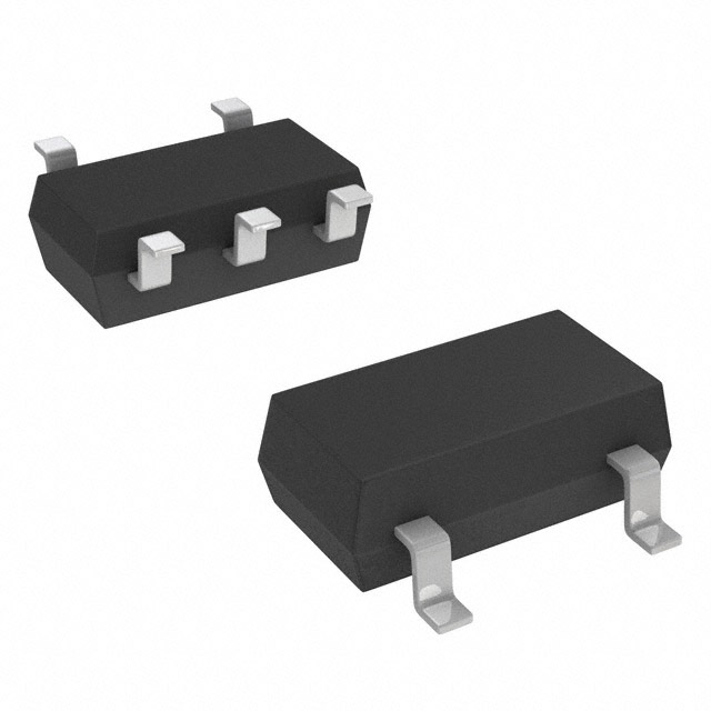
• 5-Pin SOT23 or 8-Pin SC70JW Package
Applications
The AAT4900 is available in a Pb-free 5-pin SOT23 or
8-pin SC70JW package and is specified over the -40°C to
+85°C temperature range.
• DC Motor Drive
• High Frequency DC/DC Converters
• MOSFET Driver
Typical Application
DC/DC Converter Output Stage
2.0V to 5.5V Input
IN
Control Circuit
(PWM Output)
ENABLE
CLK
EN
AAT4900
OUTPUT
LX
SOT23
GND
Skyworks Solutions, Inc. • Phone [781] 376-3000 • Fax [781] 376-3100 • sales@skyworksinc.com • www.skyworksinc.com
202217A • Skyworks Proprietary Information • Products and Product Information are Subject to Change Without Notice. • July 30, 2012
1
�DATA SHEET
AAT4900
Buffered Power Half Bridge
Pin Descriptions
Pin #
SOT23-5
SC70JW-8
Symbol
1
2
2, 3
6, 7, 8
LX
GND
3
4
EN
4
5
5
1
CLK
IN
Function
Inductor connection. LX output is controlled by CLK and EN (see Control Logic Table).
Ground connection.
Active-high enable input. A logic low signal puts the LX output pin in high impedance
mode.
Logic input signal determines the state of LX output.
Supply voltage input. Input voltage range from 2.0V to 5.5V.
Pin Configuration
SOT23-5
(Top View)
GND
2
EN
3
5
4
IN
CLK
IN
LX
LX
EN
1
2
8
7
2
2
1
1
LX
SC70JW-8
(Top View)
3
6
4
5
GND
GND
GND
CLK
Skyworks Solutions, Inc. • Phone [781] 376-3000 • Fax [781] 376-3100 • sales@skyworksinc.com • www.skyworksinc.com
202217A • Skyworks Proprietary Information • Products and Product Information are Subject to Change Without Notice. • July 30, 2012
�DATA SHEET
AAT4900
Buffered Power Half Bridge
Control Logic Table
Inputs
Output
CLK
EN
LX
0
0
1
1
0
1
0
1
High Impedance
VIN
High Impedance
Ground
Absolute Maximum Ratings1
TA = 25°C, unless otherwise noted.
Symbol
Description
VIN
VEN, VCLK
VOUT
IMAX
TJ
VESD
TLEAD
IN to GND
EN, CLK to GND
OUT to GND
Maximum Continuous Switch Current
Operating Junction Temperature Range
ESD Rating2 - HBM
Maximum Soldering Temperature (at Leads)
Value
Units
-0.3 to 6
-0.3 to 6
-0.3 to VIN+0.3
2
-40 to 150
4000
300
V
V
V
A
°C
V
°C
Value
Units
190
526
°C/W
mW
Thermal Information3
Symbol
QJA
PD
Description
Thermal Resistance (SOT23-5, SC70JW-8)
Power Dissipation (SOT23-5, SC70JW-8)
1. Stresses above those listed in Absolute Maximum Ratings may cause permanent damage to the device. Functional operation at conditions other than the operating conditions
specified is not implied. Only one Absolute Maximum Rating should be applied at any one time.
2. Human body model is a 100pF capacitor discharged through a 1.5kW resistor into each pin.
3. Mounted on a demo board.
Skyworks Solutions, Inc. • Phone [781] 376-3000 • Fax [781] 376-3100 • sales@skyworksinc.com • www.skyworksinc.com
202217A • Skyworks Proprietary Information • Products and Product Information are Subject to Change Without Notice. • July 30, 2012
3
�DATA SHEET
AAT4900
Buffered Power Half Bridge
Electrical Characteristics
VIN = 5V, TA = -40°C to +85°C, unless otherwise noted. Typical values are at TA = 25°C.
Symbol
VIN
IQAC
IQDC
IQ(OFF)
ISD(OFF)
Operation Voltage
AC Quiescent Current
DC Quiescent Current
Off-Supply Current
Off-Switch Current
RDS(ON)H
High Side MOSFET On Resistance
RDS(ON)L
Low Side MOSFET On Resistance
VONL
VONH
ISINK
CLK, EN Input Low Voltage
CLK, EN Input High Voltage
CLK, EN Input Leakage
TBBM
Break-Before-Make Time
TON-DLY
THIZ
4
Description
CLK to LX Delay
EN to OUT HiZ Delay
Conditions
Min
Typ
2.0
IN = 5V, EN = IN, CLK = 1MHz, ILX = 0
IN = 5V, EN = IN, CLK = GND, ILX = 0
EN = CLK = GND, IN = LX = 5.5V
EN = GND, IN = 5.5V, VOUT = 0 or LX = IN
IN = 5V, TA = 25°C
IN = 3V, TA = 25°C
IN = 2V, TA = 25°C
IN = 5V, TA = 25°C
IN = 3V, TA = 25°C
IN = 2V, TA = 25°C
IN = 2V to 5.5V
IN = 2V to 5.5V
CLK, EN = 5.5V
CLK Rising
CLK Falling
CLK Rising
CLK Falling
CLK = GND
CLK = IN
4
0.03
130
165
235
105
135
200
Max
Units
5.5
9
1
1
1
165
195
V
mA
µA
µA
µA
mW
145
175
mW
0.4
1.5
0.01
5
5
30
40
40
40
1
Skyworks Solutions, Inc. • Phone [781] 376-3000 • Fax [781] 376-3100 • sales@skyworksinc.com • www.skyworksinc.com
202217A • Skyworks Proprietary Information • Products and Product Information are Subject to Change Without Notice. • July 30, 2012
V
V
µA
ns
ns
ns
�DATA SHEET
AAT4900
Buffered Power Half Bridge
Typical Characteristics
Operating Current vs. Switching Frequency
Operating Current vs. Input Voltage
7
Operating Current (mA)
Operating Current (mA)
(FS = 1MHz)
6
5
4
3
2
1
0
2.5
3.0
3.5
4.0
4.5
5.0
6.0
5.5
10.000
1.000
VIN = 5V
0.100
VIN = 3V
0.010
0.001
0.000
0.0
0.1
1
Operating Current vs. Temperature
RDS(ON) (Ω)
Operating Current (mA)
8
VIN = 5.5V
4
VIN = 4.3V
2.4
2.2
2.0
0.22
0.21
0.20
0.19
0.18
0.17
0.16
0.15
0.14
0.13
0.12
0.11
0.10
0.20
0
20
40
60
80
100
120
VIN = 3.1V
1.8
1.6
1.4
VIN = 2.7V
1.2
1.0
-20
-40
-20
0
20
40
60
80
100
120
Temperature (°C)
Temperature (°C)
High Side RDS(ON) vs. Output Current
Low Side R DS(ON) vs. Output Current
0.16
VIN = 2.7V
0.15
VIN = 2.7V
0.14
RDS(ON) (Ω)
Operating Current (mA)
10
-40
10000
(FS = 1MHz)
12
0
1000
Operating Current vs. Temperature
(FS = 1MHz)
2
100
Frequency (kHz)
Input Voltage (V)
6
10
0.60
0.80
0.12
0.11
0.10
VIN = 5.5V
0.40
0.13
VIN = 5.5V
0.09
1.00
1.20
1.40
1.60
Output Current (A)
1.80
2.00
2.20
0.08
0.2
0.4
0.6
0.8
1
1.2
1.4
1.6
1.8
2
2.2
Output Current (A)
Skyworks Solutions, Inc. • Phone [781] 376-3000 • Fax [781] 376-3100 • sales@skyworksinc.com • www.skyworksinc.com
202217A • Skyworks Proprietary Information • Products and Product Information are Subject to Change Without Notice. • July 30, 2012
5
�DATA SHEET
AAT4900
Buffered Power Half Bridge
Typical Characteristics
High Side RDS(ON)
Low Side RDS(ON)
0.30
0.30
0.20
RDS(ON) (Ω)
RDS(ON) (Ω)
0.25
VIN = 2.7V,
ID = 2.2A
0.25
0.15
0.10
VIN = 2.7V,
ID = 0.2A
VIN = 5.5V,
ID = 0.2A to 2.2A
0.05
0.00
-40
-20
0
20
40
60
80
VIN = 2.7V,
ID = 2.2A
0.20
0.15
0.10
100
0.00
-40
120
VIN = 2.7V,
ID = 0.2A
VIN = 5.5V,
ID = 0.2A to 2.2A
0.05
-20
0
Temperature (°C)
20
40
60
80
100
120
Temperature (°C)
Propagation Delay vs. Input Voltage
CLK/Enable Threshold vs. Input Voltage
(CL = 1000pF)
1.4
Threshold Voltage (V)
Delay Time (ns)
120
tPLH
100
80
60
40
20
tPHL
1.5
2
2.5
3
3.5
4
4.5
5
5.5
1.2
0.8
VONL
0.6
0.4
0.2
1.5
Input Voltage (V)
VONH
1.0
2
2.5
3
3.5
4
4.5
Input Voltage (V)
RDS(ON) vs. Input Voltage
0.28
0.26
R DS(ON) (Ω)
0.24
0.22
High Side
0.20
0.18
0.16
0.14
Low Side
0.12
0.10
1.5
2
2.5
3
3.5
4
Input Voltage (V)
6
4.5
5
5.5
Skyworks Solutions, Inc. • Phone [781] 376-3000 • Fax [781] 376-3100 • sales@skyworksinc.com • www.skyworksinc.com
202217A • Skyworks Proprietary Information • Products and Product Information are Subject to Change Without Notice. • July 30, 2012
5
5.5
�DATA SHEET
AAT4900
Buffered Power Half Bridge
Functional Block Diagram
IN
CLK
Control Logic
and
Shoot-Through
Protection
LX
EN
GND
Typical Applications
Synchronous Buck
DC/DC Converter Application
DC/DC Converter
The losses associated with the AAT4900 high side
switching MOSFET are due to switching losses and conduction losses. The conduction losses are associated
with the RDS(ON) characteristics of the output switching
device. At the full load condition, assuming continuous
conduction mode (CCM), the on losses can be derived
from the following equations.
The most common AAT4900 applications include a DC/
DC converter output power stage and a MOSFET gate
drive buffer.
Figure 1 shows a common configuration when used as a
DC/DC converter power stage with synchronous rectification. The enable pin can be used to force the LX output to
a high impedance state under light load conditions. This
enables the output inductor to operate in discontinuous
conduction mode (DCM), improving efficiency under light
load conditions. The body diode associated with the low
side switching device gives the AAT4900 inductive switching capability, clamping the LX node at a diode drop below
GND during the break-before-make time.
Eq. 1: D =
VO
VIN
D is the duty cycle.
Eq. 2: ∆I =
V
VO
1- O
L · FS VIN
DI is the peak-to-peak inductor ripple current.
Skyworks Solutions, Inc. • Phone [781] 376-3000 • Fax [781] 376-3100 • sales@skyworksinc.com • www.skyworksinc.com
202217A • Skyworks Proprietary Information • Products and Product Information are Subject to Change Without Notice. • July 30, 2012
7
�DATA SHEET
AAT4900
Buffered Power Half Bridge
VIN = 2.0 to 5.5V
IN
EN
DC / DC
Controller
AAT4900
+
LX
CLK
VOUT = 0 to VIN
IOUT = 0 to 1A
GND
GND
-
Figure 1: AAT4900 DC/DC Converter Power Stage.
High Side Switch RMS Current
Eq. 3: IRMS(HS) =
2
2 ∆I
IO +
·D
12
Low Side Switch RMS Current
The low side RMS current is estimated by the following
equation.
2
2 ∆I
IO +
· (1 - D)
Eq. 4: IRMS(LS) =
12
Total Losses
quency and voltage, the bias current must be checked at
the frequency, voltage, and temperature of operation
with no load attached to the LX node. Once the above
losses have been determined, the maximum junction
temperature can be calculated.
Eq. 6: TJ(MAX) = PLOSS · ΘJC = TAMB
Using the above equations, the graph below shows the
current capability for some typical applications with
maximum junction temperatures of 150°C and 120°C.
The increase in RDS(ON) vs. temperature is estimated at
3.75mW for a 10°C increase in junction temperature.
A simplified form of the above results (where the above
descriptions of IRMS has been approximated with Io) is
given by:
1.75
IO2 · (RDS(ON)H · VO + RDS(ON)L · (VIN -VO))
VIN
+ (tsw · FS · IO + IQ) · VIN
Substitution of the IRMS equations with IO results in very
little error when the inductor ripple current is 20% to
40% of the full load current. The equation also includes
switching and quiescent current losses where tSW is
approximated at 18 nsec and IQ is the no load quiescent
current of the AAT4900. Quiescent current losses are
associated with the gate drive of the output stage and
biasing. Since the gate drive current varies with fre-
8
(FS = 1MHz)
Output Current (A)
Eq. 5: PLOSS =
Step-Down Converter Limits
VIN = 4.2V, VO = 2.5V
VIN = 5.0V, VO = 3.3V
TJMAX = 150°C
1.5
1.25
TJMAX = 120°C
1
VIN = 4.2V, VO = 2.5V
VIN = 5.0V, VO = 3.3V
0.75
0.5
25
35
45
55
65
Ambient Temperature (°C)
Skyworks Solutions, Inc. • Phone [781] 376-3000 • Fax [781] 376-3100 • sales@skyworksinc.com • www.skyworksinc.com
202217A • Skyworks Proprietary Information • Products and Product Information are Subject to Change Without Notice. • July 30, 2012
75
85
�DATA SHEET
AAT4900
Buffered Power Half Bridge
Gate Drive
Gate Drive Current Ratings
An estimate of the maximum gate drive capability with
no external series resistor can be derived from Equation
7. Note that the quiescent current varies with the ambient temperature, frequency of operation, and input voltage. The graphs below display the quiescent current and
maximum gate charge drive capability at 85°C ambient
vs. frequency for various input voltages.
1 TJ(MAX) - TAMB
- IQ
Eq. 7: QG(MAX) = F · θ · V
JA
S
IN(MAX)
1
120°C - 85°C
= 1MHz · 190°C/W · 4.2V - 3.2mA
= 40nC
The quiescent current was first measured over temperature for various input voltages with no load attached.
Equation 7 was then used to derive the maximum gate
charge capability for the desired maximum junction
temperature. QG is the gate charge required to raise the
gate of the load MOSFET to the input voltage. This value
is taken from the MOSFET manufacturer’s gate charge
curve.
100
Operating Current (mA)
The low RDS(ON) of the output stage allows for a high peak
gate current and fast switching speeds. A small package
size facilitates close placement to the power device for
optimum switching performance. The logic level inputs
(CLK and EN) are high impedance inputs.
No Load Operating Current at 85°C Ambient
VIN = 4.2V
VIN = 5.0V
10
VIN = 5.5V
VIN = 2.7V
1
0.1
100
1000
10000
Frequency (kHz)
Maximum Gate Charge Load @ 85°C
(Ambient TJ(MAX) = 120°C)
1000
Gate Charge (nC)
When used as a MOSFET gate driver, the break-beforemake shoot-through protection significantly reduces
losses associated with the driver at high frequencies.
(See Figure 2.)
VIN = 2.7V
100
VIN = 4.2V
10
VIN = 5.0V
VIN = 5.5V
1
100
1000
10000
Frequency (kHz)
+5V
Load
Circuit
IN
Enable
EN
AAT4900
Clock
LX
CLK
GND
Ground
Figure 2: AAT4900 Gate Drive Configuration.
Skyworks Solutions, Inc. • Phone [781] 376-3000 • Fax [781] 376-3100 • sales@skyworksinc.com • www.skyworksinc.com
202217A • Skyworks Proprietary Information • Products and Product Information are Subject to Change Without Notice. • July 30, 2012
9
�DATA SHEET
AAT4900
Buffered Power Half Bridge
Motor Drive
Recommended Decoupling
Layout Pattern
The AAT4900 is also ideally suited for use as an efficient
output driver for DC brushless motor control. The inductive load switching capability of the AAT4900 eliminates
the need for external diodes. A typical motor control
circuit is illustrated in Figure 3.
Because of the extremely fast switching speed and the
high switching currents, optimum placement of the input
capacitor is critical. It is recommended that a 0.1µF to
10µF 0805 or 1206 ceramic capacitor be placed as close
as possible to the IC, as shown in Figure 4. This helps to
decouple the switching transients from the stray inductance present in the PC board.
Enable
+5V
IN
EN
IN
AAT4900
Clock
LX
LX
CLK
DC Brushless
Motor
GND
EN
AAT4900
CLK
GND
Ground
Figure 3: Typical Motor Control Block Diagram.
AAT4900
4 CLK
3 EN
2 GND
1 LX
5 V+
CAP
Figure 4: Recommended Decoupling Layout Pattern.
10
Skyworks Solutions, Inc. • Phone [781] 376-3000 • Fax [781] 376-3100 • sales@skyworksinc.com • www.skyworksinc.com
202217A • Skyworks Proprietary Information • Products and Product Information are Subject to Change Without Notice. • July 30, 2012
�DATA SHEET
AAT4900
Buffered Power Half Bridge
CLK
LX
Figure 5: Timing Diagram.
50%
CLK
50%
tPHL
tPLH
tf
90%
LX
10%
Figure 6: Switching Time Waveforms.
VIN
10µF
IN
EN
LX
1000pF
CLK
GND
Figure 7: Propagation Delay Test Circuit.
Skyworks Solutions, Inc. • Phone [781] 376-3000 • Fax [781] 376-3100 • sales@skyworksinc.com • www.skyworksinc.com
202217A • Skyworks Proprietary Information • Products and Product Information are Subject to Change Without Notice. • July 30, 2012
11
�DATA SHEET
AAT4900
Buffered Power Half Bridge
Ordering Information
Package
Marking1
Part Number (Tape and Reel)2
SOT23-5
SC70JW-8
ABXYY
ABXYY
AAT4900IGV-T1
AAT4900IJS-T1
Skyworks Green™ products are compliant with
all applicable legislation and are halogen-free.
For additional information, refer to Skyworks
Definition of Green™, document number
SQ04-0074.
Package Information
SOT23-5
2.85 ± 0.15
1.90 BSC
0.40 ± 0.10
0.075 ± 0.075
0.15 ± 0.07
4° ± 4°
10° ± 5°
1.10 ± 0.20
0.60 REF
1.20 ± 0.25
2.80 ± 0.20
1.575 ± 0.125
0.95
BSC
0.60 REF
0.45 ± 0.15
GAUGE PLANE
0.10 BSC
All dimensions in millimeters.
1. XYY = assembly and date code.
2. Sample stock is generally held on part numbers listed in BOLD.
12
Skyworks Solutions, Inc. • Phone [781] 376-3000 • Fax [781] 376-3100 • sales@skyworksinc.com • www.skyworksinc.com
202217A • Skyworks Proprietary Information • Products and Product Information are Subject to Change Without Notice. • July 30, 2012
�DATA SHEET
AAT4900
Buffered Power Half Bridge
SC70JW-8
2.20 ± 0.20
1.75 ± 0.10
0.50 BSC 0.50 BSC 0.50 BSC
0.225 ± 0.075
2.00 ± 0.20
0.100
0.15 ± 0.05
0.45 ± 0.10
4° ± 4°
0.05 ± 0.05
7° ± 3°
1.10 MAX
0.85 ± 0.15
0.048REF
2.10 ± 0.30
All dimensions in millimeters.
Copyright © 2012 Skyworks Solutions, Inc. All Rights Reserved.
Information in this document is provided in connection with Skyworks Solutions, Inc. (“Skyworks”) products or services. These materials, including the information contained herein, are provided by Skyworks as a
service to its customers and may be used for informational purposes only by the customer. Skyworks assumes no responsibility for errors or omissions in these materials or the information contained herein. Skyworks may change its documentation, products, services, specifications or product descriptions at any time, without notice. Skyworks makes no commitment to update the materials or information and shall have no
responsibility whatsoever for conflicts, incompatibilities, or other difficulties arising from any future changes.
No license, whether express, implied, by estoppel or otherwise, is granted to any intellectual property rights by this document. Skyworks assumes no liability for any materials, products or information provided hereunder, including the sale, distribution, reproduction or use of Skyworks products, information or materials, except as may be provided in Skyworks Terms and Conditions of Sale.
THE MATERIALS, PRODUCTS AND INFORMATION ARE PROVIDED “AS IS” WITHOUT WARRANTY OF ANY KIND, WHETHER EXPRESS, IMPLIED, STATUTORY, OR OTHERWISE, INCLUDING FITNESS FOR A PARTICULAR
PURPOSE OR USE, MERCHANTABILITY, PERFORMANCE, QUALITY OR NON-INFRINGEMENT OF ANY INTELLECTUAL PROPERTY RIGHT; ALL SUCH WARRANTIES ARE HEREBY EXPRESSLY DISCLAIMED. SKYWORKS DOES
NOT WARRANT THE ACCURACY OR COMPLETENESS OF THE INFORMATION, TEXT, GRAPHICS OR OTHER ITEMS CONTAINED WITHIN THESE MATERIALS. SKYWORKS SHALL NOT BE LIABLE FOR ANY DAMAGES, INCLUDING BUT NOT LIMITED TO ANY SPECIAL, INDIRECT, INCIDENTAL, STATUTORY, OR CONSEQUENTIAL DAMAGES, INCLUDING WITHOUT LIMITATION, LOST REVENUES OR LOST PROFITS THAT MAY RESULT FROM
THE USE OF THE MATERIALS OR INFORMATION, WHETHER OR NOT THE RECIPIENT OF MATERIALS HAS BEEN ADVISED OF THE POSSIBILITY OF SUCH DAMAGE.
Skyworks products are not intended for use in medical, lifesaving or life-sustaining applications, or other equipment in which the failure of the Skyworks products could lead to personal injury, death, physical or environmental damage. Skyworks customers using or selling Skyworks products for use in such applications do so at their own risk and agree to fully indemnify Skyworks for any damages resulting from such improper
use or sale.
Customers are responsible for their products and applications using Skyworks products, which may deviate from published specifications as a result of design defects, errors, or operation of products outside of published parameters or design specifications. Customers should include design and operating safeguards to minimize these and other risks. Skyworks assumes no liability for applications assistance, customer product
design, or damage to any equipment resulting from the use of Skyworks products outside of stated published specifications or parameters.
Skyworks, the Skyworks symbol, and “Breakthrough Simplicity” are trademarks or registered trademarks of Skyworks Solutions, Inc., in the United States and other countries. Third-party brands and names are for
identification purposes only, and are the property of their respective owners. Additional information, including relevant terms and conditions, posted at www.skyworksinc.com, are incorporated by reference.
Skyworks Solutions, Inc. • Phone [781] 376-3000 • Fax [781] 376-3100 • sales@skyworksinc.com • www.skyworksinc.com
202217A • Skyworks Proprietary Information • Products and Product Information are Subject to Change Without Notice. • July 30, 2012
13
�


 工商网监
湘ICP备2023018690号
工商网监
湘ICP备2023018690号
