Si3452/3
Q U A D H IGH - VOLTAGE P O R T C O NT R O L L E R F O R P O E A N D P O E + P S E S
Features
Power over Ethernet Endpoint
switches and Midspans for IEEE Std
802.3af and 802.3at
Supports high power PDs, such as:
Pan/Tilt/Zoom security cameras
802.11n WAPs
Multi-band, multi-radio WAPs
Security and RFID systems
Rev. 0.47 10/09
Copyright © 2009 by Silicon Laboratories
Industrial automation systems
Networked audio
IP Phone Systems and iPBXs
Metropolitan area networked WAPs,
cameras, and sensors
WiMAX ASN/BTS and CPE/ODU
systems
See page 30.
Pin Assignments
INT
VOUT1
RST
DET1
AD1
GND12
AD0
DET2
VOUT2
VEE2
40
39
38
37
36
35
34
33
32
31
40-pin QFN
VEE1
1
30
VDD
VEE
2
29
DGND
VREF
3
28
AD0
AIN
4
27
AD1
AOUT
5
26
AD2
AGND
6
25
AD2
RBIAS
7
24
AD3
AGND
8
23
RST
NC
9
22
VEE3
VEE4
10
21
AD3
13
14
15
16
17
18
19
20
DET4
SDA
GND34
SCL
NC
DET3
VDD
VOUT3
Si3452
(Top View)
12
Applications
Ordering Information:
11
Programmable architecture supports
IEEE 802.3af (PoE) and IEEE
802.3at (PoE+) PSEs
Programmable current limits for
PoE (350 mA) and PoE+
(600 mA), and custom limits to
850 mA
Per-port current and voltage
monitoring for sophisticated power
management and control
Power policing mode
Robust multi-point detection
Supports 1-Event and 2-Event
classification algorithms
Comprehensive, robust, faultprotection circuitry
Supply under-voltage lockout
(UVLO)
Output current limit and shortcircuit protection
Foldback current limiting
Dual-threshold thermal overload
protection
Fault source reporting for
intelligent port management
Extended commercial (–10 to 85 °C)
and industrial (–40 to 85 °C)
operating temperatures
Compact, 6×6 mm2, 40-pin QFN
RoHS-compliant package
NC
Each Si3452/3 high-voltage port
controller supports four PSE power
interfaces
Programmable current limits for PoE
(15.4 W), PoE+ (30 W), and
proprietary systems (up to 40 W) per
port
I2C interface requires no external
MCU for easy, low-cost management
of 4 to 48 ports by the host system
Unique high-voltage component
integration simplifies design, lowers
power dissipation, minimizes
external BOM, and reduces PCB
footprint
Internal low-RON power FETs with
current-sense circuitry
Integrated transient voltage surge
suppressors
DC disconnect (Si3453) or
proprietary dV/dt disconnect
(Si3452) sensing methods
VOUT4
See "9. Pin Descriptions" on page 27.
Si3452/3
�Si3452/3
Description
When connected directly to the host system or configured in Auto mode, each Si3452/3 high-voltage port controller
provides all of the critical circuitry and sophisticated power measurement functionality for the high-voltage
interfaces of four complete PSE ports. The Si3452/3 fully integrates robust, low-RON (0.3 typical) power
MOSFET switches, low-power dissipation current sensing circuitry, and transient voltage surge suppression
devices.
The on-chip current sense circuitry and power MOSFETs provide programmable scaling of current limits to match
either PoE (350 mA, 15.4 W), PoE+ (600 mA, 30 W), and extended (800 mA, 40 W) power requirements on a perport basis. Designed for use in Endpoint PSE (e.g., Ethernet switches) or Midspan PSE (e.g., inline power
injectors) applications, each Si3452/3 also performs the IEEE-required powered device (PD) detection,
classification, and disconnect functionality.
The flexible architecture enables powered device disconnect detection using either dc disconnect (Si3453) or
Silicon Laboratories' proprietary dV/dt disconnect (Si3452) sensing algorithm. dV/dt disconnect is an alternative to
dc disconnect that requires no additional BOM components, does not dissipate extra device power, and fully
interoperates with all powered devices. Also provided are multi-point detection algorithms and per-port current and
voltage monitoring.
Intelligent protection circuitry includes power supply under-voltage lockout (UVLO), port output current limiting and
short-circuit protection, thermal overload sensing and port shutdown, and transient voltage surge-suppressors
capable of protecting the Si3452/3 from a variety of harsh surge events seen on the RJ-45 interface.
To maximize system design flexibility and minimize cost, each Si3452/3 connects directly to a system host
controller through an I2C serial interface, eliminating the need for an external MCU. The Si3452/3 can be set to one
of 12 unique addresses, allowing control of up to 48 ports on a single I2C bus.
PER PORT ANALOG
Detection
&
Classification
256 Byte SRAM
MEAS.
MUX
Temp
Sensor
2
DET2
DET1
Rev. 0.47
VOUT4
VOUT3
VOUT2
Thermal
Prot.
Current
Sense
VOUT1
VEE4
VEE
DGND
VDD
VREF
RBIAS
AOUT
DET3
Gate Control,
Current Limit
& Foldback
VREF & Central Bias
AIN
SCL
SDA
INT
I2C
VDD
Voltage
Regulator
& Monitor
AGND
WDT
AMUX
PGA
DET4
DC or
dV/dt
Disconnect
VEE3
POR
AGND
PLL
10b
ADC
Channel
Mode
&
Limit
Control
VEE1
8 kByte EPROM
GND12
GND34
AD0
AD1
AD2
AD3
RST
AD1
AD0
HV SPI
&
Port
Control
LV SPI
VEE2
MCU Core
& PSE FSM
AD2
AD3
RST
Functional Block Diagram
�Si3452/3
TABLE O F C ONTENTS
Section
Page
1. Electrical Specifications . . . . . . . . . . . . . . . . . . . . . . . . . . . . . . . . . . . . . . . . . . . . . . . . . . .4
2. PSE System-Level Diagrams . . . . . . . . . . . . . . . . . . . . . . . . . . . . . . . . . . . . . . . . . . . . . . . 11
3. PSE Application Diagrams . . . . . . . . . . . . . . . . . . . . . . . . . . . . . . . . . . . . . . . . . . . . . . . . 11
4. Functional Description . . . . . . . . . . . . . . . . . . . . . . . . . . . . . . . . . . . . . . . . . . . . . . . . . . . 12
4.1. Detection . . . . . . . . . . . . . . . . . . . . . . . . . . . . . . . . . . . . . . . . . . . . . . . . . . . . . . . . . . 12
4.2. Classification . . . . . . . . . . . . . . . . . . . . . . . . . . . . . . . . . . . . . . . . . . . . . . . . . . . . . . . 13
4.3. Port Turn-On and Power FETs . . . . . . . . . . . . . . . . . . . . . . . . . . . . . . . . . . . . . . . . . 13
4.4. Disconnect Detection . . . . . . . . . . . . . . . . . . . . . . . . . . . . . . . . . . . . . . . . . . . . . . . . 14
4.5. Transient Voltage Surge Suppression . . . . . . . . . . . . . . . . . . . . . . . . . . . . . . . . . . . 14
4.6. Temperature Sense . . . . . . . . . . . . . . . . . . . . . . . . . . . . . . . . . . . . . . . . . . . . . . . . . 14
4.7. Port Measurement and Monitoring . . . . . . . . . . . . . . . . . . . . . . . . . . . . . . . . . . . . . .14
4.8. SMBus/I2C Interface Description . . . . . . . . . . . . . . . . . . . . . . . . . . . . . . . . . . . . . . . 15
5. Register Interface . . . . . . . . . . . . . . . . . . . . . . . . . . . . . . . . . . . . . . . . . . . . . . . . . . . . . . . .17
5.1. Interrupt (Registers 0x00–0x01) . . . . . . . . . . . . . . . . . . . . . . . . . . . . . . . . . . . . . . . . 17
5.2. Port Event (Registers 0x02–0x05) . . . . . . . . . . . . . . . . . . . . . . . . . . . . . . . . . . . . . .17
5.3. Port Status (Registers 0x06–0x09) . . . . . . . . . . . . . . . . . . . . . . . . . . . . . . . . . . . . . . 17
5.4. Port Configuration (Registers 0x0A–0x11) . . . . . . . . . . . . . . . . . . . . . . . . . . . . . . . . 18
5.5. Command and Return Registers (Registers 0x12–0x1C) . . . . . . . . . . . . . . . . . . . . .19
5.6. Device Status Register (0x1D) . . . . . . . . . . . . . . . . . . . . . . . . . . . . . . . . . . . . . . . . . 19
6. Operational Notes . . . . . . . . . . . . . . . . . . . . . . . . . . . . . . . . . . . . . . . . . . . . . . . . . . . . . . . 24
6.1. Port Turn On . . . . . . . . . . . . . . . . . . . . . . . . . . . . . . . . . . . . . . . . . . . . . . . . . . . . . . .24
6.2. Changing the Interrupt Mask . . . . . . . . . . . . . . . . . . . . . . . . . . . . . . . . . . . . . . . . . . . 24
6.3. Port Voltage and Current Measurements . . . . . . . . . . . . . . . . . . . . . . . . . . . . . . . . . 24
7. PCB Layout Guidelines . . . . . . . . . . . . . . . . . . . . . . . . . . . . . . . . . . . . . . . . . . . . . . . . . . .25
8. Firmware Release Notes . . . . . . . . . . . . . . . . . . . . . . . . . . . . . . . . . . . . . . . . . . . . . . . . . . 26
8.1. Initialization Time . . . . . . . . . . . . . . . . . . . . . . . . . . . . . . . . . . . . . . . . . . . . . . . . . . .26
8.2. Current Limiting in 2x Power Mode . . . . . . . . . . . . . . . . . . . . . . . . . . . . . . . . . . . . . . 26
8.3. I2C Address ACK . . . . . . . . . . . . . . . . . . . . . . . . . . . . . . . . . . . . . . . . . . . . . . . . . . . 26
9. Pin Descriptions . . . . . . . . . . . . . . . . . . . . . . . . . . . . . . . . . . . . . . . . . . . . . . . . . . . . . . . . . 27
10. Package Outline: 40-Pin QFN . . . . . . . . . . . . . . . . . . . . . . . . . . . . . . . . . . . . . . . . . . . . .30
11. Recommended PCB Footprint . . . . . . . . . . . . . . . . . . . . . . . . . . . . . . . . . . . . . . . . . . . . 31
12. Ordering Guide . . . . . . . . . . . . . . . . . . . . . . . . . . . . . . . . . . . . . . . . . . . . . . . . . . . . . . . . . 33
12.1. Evaluation Kits and Reference Designs . . . . . . . . . . . . . . . . . . . . . . . . . . . . . . . . . 33
13. Device Marking Diagram . . . . . . . . . . . . . . . . . . . . . . . . . . . . . . . . . . . . . . . . . . . . . . . . . 34
Document Change List . . . . . . . . . . . . . . . . . . . . . . . . . . . . . . . . . . . . . . . . . . . . . . . . . . . . .35
Contact Information . . . . . . . . . . . . . . . . . . . . . . . . . . . . . . . . . . . . . . . . . . . . . . . . . . . . . . . .36
Rev. 0.47
3
�Si3452/3
1. Electrical Specifications
Unless noted otherwise, specifications apply over the operating temperature range with VDD = +3.3 V and
VEE = –48 V relative to GND.
VDD pins should be electrically shorted. AGND pins, DGND, GND12, and GND34 should be electrically shorted
("GND"). VEE, VEE1, VEE2, VEE3, and VEE4 should be electrically shorted ("VEE").
VPort for any port is measured from GND to the respective VOUTn.
Table 1. Absolute Maximum Ratings1
Type
Description
Rating
Unit
Supply voltages
VEE to GND
–62 to +0.3
V
VDD to GND
–0.3 to +3.6
V
VDD1 to VDD2
–0.3 to +0.3
V
Any VEE to any other VEE
–0.3 to +0.3
V
Any GND to any other GND
–0.3 to +0.3
V
Voltage on digital pins
SDA, SCL, ADn, RST, INT
(GND – 0.3) to (VDD + 0.3)
V
Voltage on analog pins
VREF, AIN, AOUT, RBIAS, OSC
(GND – 0.3) to (VDD + 0.3)
V
VOUTn, DETn
(VEE – 0.3) to (GND + 0.3)
V
DETn peak currents during surge events2
±5
A
Maximum continuous power dissipation3
1.2
W
Maximum junction temperature
125
°C
–55 to 150
°C
260
°C
Ambient storage temperature
Lead temperature (soldering, 10 seconds maximum)
Notes:
1. Functional operation should be restricted to those conditions specified in Table 2. Functional operation or specification
compliance is not implied at these conditions. Stresses beyond those listed in absolute maximum ratings may cause
permanent damage to the device.
2. See IEEE Std 802.3-2005, clause 33.4, for a description of surge events.
3. If all ports are on with 600 mA load, the power dissipation is 25 °C, –35 V over the full temperature range.
2. 1x mode current limit is enforced during the 60 ms TSTART time.
3. In auto mode, class policing is automatically enabled. In manual mode, ICUT must be programmed manually.
See "5.4. Port Configuration (Registers 0x0A–0x11)" on page 18 for more information.
4. 600 mA is consistent with the IEEE 802.3at draft standard. ICUT is user-programmable in 3.2 mA increments to over
800 mA for non-standard applications.
5. For 2x mode and extreme overload or short-circuit events, TOVLD will dynamically decrease to prevent excessive FET
heating. This is consistent with the 802.3at draft.
Table 7. DC- and dV/dt Disconnect Specifications
Description
Symbol
Load current to prevent
disconnect
ION
Load current to
guarantee disconnect
IOFF
Disconnect delay
TDCDV_DLY
Test Conditions
Min
Typ
Max
Unit
10
—
—
mA
dc disconnect
—
—
5
mA
dV/dt disconnect
—
—
2
mA
Time from IOFF load current to port
turn off
300
—
400
ms
Rev. 0.47
7
�Si3452/3
Table 8. Port Measurement and Monitoring Specifications
Description
Symbol
Test Conditions
Min
Typ
Max
Unit
Port current measurement
offset
IOFFSET
–5
—
5
mA
Port current measurement
tolerance
%TOL
20 mA ≤ IPORT ≤ ICUT. For final
IPORT reading, add offset to % of
reading tolerance.
–4
—
4
%
Test Conditions
Min
Typ
Max
Unit
SCL, SDA pins Tj < –10 °C
—
—
0.85
V
Table 9. SMBus (I2C) Electrical Specifications
VDD = 3.0 to 3.6 V
Description
Input low voltage
Symbol
VIL
SCL, SDA pins over full temp range
0.8
Input high voltage
VIH
SCL, SDA pins
2.2
—
—
V
Output low voltage
VOL
SCL, SDA pins,
driving ≤ 8.5 mA
—
—
0.6
V
IL
SCL, SDA pins
—
—
40
µA
Input leakage current
Table 10. Address Pin Electrical Specifications*
VDD = 3.0 to 3.6 V
Description
Symbol
Test Conditions
Min
Typ
Max
Unit
Input low voltage
VIL
AD0, AD1, AD2, AD3 pins
—
—
0.8
V
Input high voltage
VIH
AD0, AD1, AD2, AD3 pins
0.7 x VDD
—
—
V
IH, IL
AD0, AD1, AD2, AD3 pins
–10
—
10
µA
Input leakage current
*Note: At power-up, these pins are logic inputs. A 10 k pull up or pull down resistor is used for address selection. After
address recognition, the pins are used for internal communications.
8
Rev. 0.47
�Si3452/3
Table 11. SMBus (I2C) Timing Specifications (see Figure 1)
VDD = 3.0 to 3.6 V
Description
Symbol
Test Conditions
Min
Typ
Max
Unit
Serial bus clock frequency
fSCL
0
—
400
kHz
SCL high time
tSKH
600
—
—
ns
SCL low time
tSKL
1.3
—
—
μs
SCL, SDA rise time
tR_SCL
20
—
300
ns
SCL, SDA fall time
tF_SCL
20
—
150
ns
Bus free time
tBUF
Between START and STOP
conditions.
1.3
—
—
μs
Start hold time
tSTH
Between START and first low SCL.
600
—
—
ns
Start setup time
tSTS
Between SCL high and START
condition.
600
—
—
ns
Stop setup time
tSPS
Between SCL high and STOP
condition.
600
—
—
ns
Data hold time
tDH
200
—
—
ns
Data setup time
tDS
200
—
—
ns
—
—
100
ms
—
—
5
ms
Time from hardware or software reset until start of I2C
traffic
tRESET
Delay from event to INT pin
low or from clear-on-read to
INT pin high
tINT
Reset to start condition
Notes:
1. Not production tested (guaranteed by design).
2. All timing references measured at VIL and VIH.
3. The Si3452/3 will stretch (pull down on) SCK during the ACK time period if required. The maximum SCL stretching is
10 µsec; so, SCL only needs to be bidirectional for I2C bus speeds over 50 kHz.
t R_SCL
fSC L
t F_SC L
t SKH
tSKL
SCL
tBU F
tST H
SDA
t DS
D7
D6
tD H
D5
Start Bit
D4
tSPS
D3
D0
Stop Bit
Rev. 0.47
9
�Si3452/3
Figure 1. I2C Timing Diagram
Table 12. Interrupt (INT) Specifications
Description
Symbol
Test Conditions
Min
Typ
Max
Unit
VOL
INT pin driving ≤ 8.5 mA
—
—
0.6
V
Min
Typ
Max
Unit
Nominal VREF input
—
1.1
—
V
Reference tolerance
—
—
1
%
–10
—
+10
µA
Output low voltage
Table 13. Input Voltage Reference Specifications
Description
VREF loading
10
Symbol
Test Conditions
Input current
Rev. 0.47
�Si3452/3
I2C
SCL
Host
Controller
I2C
INT
Si8405 Digital
Isolator
OTP
RST
RAM
PSE State
Machines
and
Measurement
Subsystem
Mixed Signal
Resources
High Voltage Interface
SDA
4 Ports of PoE+
2. PSE System-Level Diagrams
Si3452/3
Figure 2. 4-Port System with Direct Host Connection
3. PSE Application Diagrams
+3.3 V
Tie high
or low to
select
address
Si8405
Bidirectional
Isolator
AD0
AD1
AD2
AD3
AD0
AD1
AD2
AD3
4x10 k
VDD
AGND DGND
GND12/34
SCL
SDA
INT
DET4
Si3452/3
RST
DET2
VREF
1.1 V
(e.g. TLV431)
DET3
DET1
RBIAS
44.2 k
1%
VEE VEE[4:1] VOUT4 VOUT3 VOUT2 VOUT1
To Magnetics
Host / Switch
PORT1
PORT2
PORT3
PORT4
–54 V
Figure 3. 4-Port Application Diagram Using DC– or dV/dt Disconnect and I2C Host Interface
Rev. 0.47
11
�Si3452/3
4. Functional Description
Integrating four independent, high-voltage PSE port interfaces, the Si3452/3 high-voltage port controller enables
an extremely flexible solution for virtually any PoE or PoE+ PSE application. The Si3452/3 provides all of the highvoltage Power over Ethernet PSE functions.
Each port of the Si3452/3 integrates all high-voltage PSE controller functions needed for a quad-port PoE design,
including the power MOSFET, efficient current-sensing circuitry, transient voltage surge suppressor, and multiple
detect and disconnect circuits. When the dc disconnect or dV/dt disconnect sensing methods are selected, the
external BOM is typically only a single filter capacitor on each high-voltage port.
When a PD device has been properly detected and classified, the port is powered by a –54 V nominal supply with
continuous monitoring of voltage and current for feedback to the host system.
In addition to the required IEEE features, the Si3452/3 includes many additional features:
Per port current / voltage monitoring and measurement
Support for 1-Event and 2-Event classification algorithms
Start up in shutdown or auto mode
Alternative A (typically used for endpoint systems) or Alternative B (typically used for midspan systems)
detection timing
4.1. Detection
The Si3452/3 has per-port signature detection that satisfies the IEEE Std 802.3™-2005 specifications. However, by
utilizing a 3-point voltage-forced detection method, the Si3452/3 yields robust recognition of valid and invalid
powered device (PD) signatures, properly identifying signatures often mischaracterized by other detection
techniques.
3 point
detection
2 event
classification
Port powerup
Figure 4. PSE Sequencing
(3-Point Detection followed by 2-Event Classification and Powerup)
Vport Relative to GND
The detection circuitry performs the function of setting the output voltage on any channel to the proper value for
detection or classification and then measuring the resulting line current.
A typical detection cycle consists of applying 4 V, then 8 V, and back to 4 V, with the current limit set to 3 mA. The
current is measured after an appropriate settling time. For a valid PD, the detection signature must be compliant
with the detection voltage both increasing and decreasing.
12
Rev. 0.47
�Si3452/3
4.2. Classification
Following a successful PD detection, the classification phase will be automatically initiated in all operational
modes. During this phase, a single measurement will be made at 18 V to determine how much power the PD
device will draw under maximum loads per the IEEE 802.3af and 802.3at standards. The current limit during this
test mode is 60 mA nominal.
The Si3452/3 supports 1-Event and 2-Event classification. When operating in PoE (15.4 W) mode results in 2-Event classification probes. The 1-Event
classification is compliant to IEEE standard 802.3-2005. 2-Event classification is compliant to draft IEEE P802.3at.
4.3. Port Turn-On and Power FETs
The FET is turned on with a gate drive that results in a very low-noise turn-on waveform with a slew rate of less
than 1 V/µsec (See Figure 5).
The power FET switch on each port has been sized to have a typical ON resistance of approximately 0.3 . The
shunt resistor for current measurement has also been set to 0.1 . Including interconnection and process variation,
the total resistance to VEE for a port that is on is 0.6 (max). This limits the maximum power dissipation per
channel to < 250 mW when the operating current is 600 mA, the maximum current allowed by the IEEE 802.3at
PoE+ standard.
The FET has a programmable operating current limit. Each channel can be set to support output currents of
400 mA or 800 mA minimum.
In addition to the normal current limit, there is a short circuit current shutdown approximately 25% greater than the
nominal current limit. If there is a transient current surge where the current ramps up faster than the programmed
current limit can respond, the gate drive voltage is clamped immediately to VEE. The clamp is enabled for at least
10 µs, which allows the normal current circuitry to respond.
Another important protection feature is foldback current limiting. When VOUT is near VEE, the current limit is at
maximum. As the VDS of the driver switch increases (and VOUT is closer to ground), the current limit goes to its
lowest level. The amount of the foldback current is scaled proportionally with the programmed current limit.
Figure 5. Turn-On Waveform—Vport Relative to GND
Rev. 0.47
13
�Si3452/3
4.4. Disconnect Detection
4.4.1. dV/dt Disconnect (Si3452)
The dV/dt disconnect function can be used to detect a disconnected device without using dc disconnect or ac
disconnect.
In dV/dt disconnect mode, the FET current limit is switched to 7.5 mA. If the voltage across the FET increases, a
load is assumed to be present, and the FET current limit is automatically switched back to its pre-selected value. If,
after 350 ms, the FET voltage has not increased, there is no load present, and the FET is turned off.
In addition to operating in a manner functionally distinct from DC disconnect, dV/dt disconnect requires no
additional external components and fully interoperates with all powered device DC Maintain Power Signatures. For
more information, see "AN399: dV/dt Disconnect and the IEEE 802.3 PoE Standard".
4.4.2. DC Disconnect (Si3453)
The port current is continuously monitored by the Si3452/3. The Si3452/3 can dynamically change the
measurement scale to achieve accuracy over a wide range of currents.
As defined in the IEEE 802.3 PoE standard, the PSE should disconnect if the port current is less than a nominal
7.5 mA for more than 350 ms.
4.5. Transient Voltage Surge Suppression
The Si3452/3 features robust on-chip surge protectors on each port; this is an industry first. This unique protection
circuitry acts as an active device that can withstand lightning-induced transients as well as large ESD transient
events. When the port voltage exceeds its protection limit and the current reaches a triggering threshold, current is
shunted from the port to the ground pins.
Internal circuitry is provided to protect the line outputs from externally-coupled fault currents. These are transient
currents of up to 5 A peak.
The operation of the protection circuits depends on the operating mode of the channel switch and the direction of
the fault current. The clamping operation is performed on the detect pin.
The switch itself will also be protected by the current limit. If the transient lasts long enough to heat up the die, then
the temperature sense circuit will shut off the switch, and all the fault current will flow through the clamp diode.
4.6. Temperature Sense
A temperature sense signal is used in conjunction with the current limit status signals from the gate drive blocks.
Any channel that is generating excess heat is assumed to be operating in current limit mode, with both high voltage
drop and high current.
If the port is in PoE mode, an overload will generally not result in thermal shutdown before the 60 ms ICUT period. If
the port is in PoE+ mode, an overload may cause the port to shut down prior to the 60 ms ICUT period. In either
case, the event is reported as ICUT. The faster shutdown in PoE+ mode is consistent with and specifically allowed
by the 802.3at draft and provides much more robust overload protection than is possible with external FETs.
In addition, there is a thermal shutdown if the package temperature exceeds 120 °C. If this threshold is reached, all
output drivers are turned off and detection modes are disabled. This secondary threshold limit guards against the
possibility that the overheating is not caused by a driver operating in current limit.
4.7. Port Measurement and Monitoring
VEE monitoring in conjunction with port current monitoring allows measurement of port power. Port power
monitoring, dynamic power allocation via LLDP*, and port power policing allow efficient power supply sizing.
The Si3452/3 is factory-calibrated and temperature-compensated for the following measurements:
Port current measurement. These measurements are auto-ranged and scaled to a 16 bit number at 100 µA per
bit. Port current accuracy is ±4% ± 2 mA.
VEE is measured with a scale of 64 V. The measurement is reported as a 16-bit number scaled at 1 mV per bit.
VEE measurement accuracy is ±4% over the valid VEE range.
*Note: LLDP = Link Layer Discovery Protocol. Refer to IEEE 802.3at (draft) and IEEE 802.1AB for more information.
14
Rev. 0.47
�Si3452/3
4.8. SMBus/I2C Interface Description
The I2C interface is a two-wire, bidirectional serial bus. The I2C is compliant with the System Management Bus
Specification (SMBus), version 1.1 and compatible with the I2C serial bus. Reads and writes to the interface by the
system controller are byte-oriented with the I2C interface autonomously controlling the serial transfer of the data. A
method of extending the clock-low duration is available to accommodate devices with different speed capabilities
on the same bus. The I2C provides control of SDA (serial data), SCL (serial clock) generation and synchronization,
arbitration logic, and START/STOP control and generation.
A typical I2C transaction consists of a START condition followed by an address byte (Bits7–1: 7-bit slave address;
Bit0: R/W direction bit), one or more bytes of data, and a STOP condition. Each byte that is received (by a master
or slave) must be acknowledged (ACK) with a low SDA during a high SCL (see Figure 6). If the receiving device
does not ACK, the transmitting device will read a NACK (not acknowledge), which is a high SDA during a high
SCL.
The direction bit (R/W) occupies the least-significant bit position of the address byte. The direction bit is set to logic
1 to indicate a "READ" operation and cleared to logic 0 to indicate a "WRITE" operation. All transactions are
initiated by a master, with one or more addressed slave devices as the target. The master generates the START
condition and then transmits the slave address and direction bit. If the transaction is a WRITE operation from the
master to the slave, the master transmits the data one byte at a time, waiting for an ACK from the slave at the end
of each byte.
For READ operations, the slave transmits the data waiting for an ACK from the master at the end of each byte. At
the end of the data transfer, the master generates a STOP condition to terminate the transaction and free the bus.
Figure 6 illustrates a typical SMBus/I2C transaction.
Silicon Laboratories recommends the use of bidirectional digital isolators, such as the Si840x, to isolate the I2C
communications interface between the Si3452/3 high-voltage port controllers and the system host controller.
Slave Addr ess
0
1
0
A3
A2 A1
ST ART
Register Address
A0 R/W#
A7
A6 A5
A4 A3 A2
ACK by IC
F ixed IC
Address
Write Data
A1 A0
D7 D6 D5 D4 D3 D2 D1 D0
ACK by IC
ACK by IC
Write Sequence
Pin Set IC
Address
Setup Register Addr ess
0
1
0
A3 A2
A1 A0 R/W#
ACK by IC
Fixed IC
Addr ess
Pin Set IC
Addr ess
Transfer Data to Setup Address
Register Address
Slave Address
START
ST OP by Master
A7 A6
A5 A4
Register Data
Slave Address
A3 A2 A1
A0
0
1
0
A3
A2 A1
ACK by IC
START
A0 R/W#
ACK by IC
F ixed IC
Address
Read Sequence
D7 D6 D5 D4 D3 D2 D1 D0
Not ACK by Master
STOP by Master
Pin Set IC
Addr ess
Figure 6. Typical I2C Bus Transactions
The Si3452 does not support the alert response address (ARA) protocol. Polling is used to determine which
controller is interrupting in an interrupt-driven system.
Rev. 0.47
15
�Si3452/3
4.8.1. Address Pins
Table 14. Address Pin Assignment
Pin #
Pin Name
21
AD3
24
AD3
25
AD2
26
AD2
27
AD1
28
AD0
34
AD0
36
AD1
Pins with the same name must be externally connected and then tied high or low via a weak (10 k) pull up or pull
down to establish the device address at power up. The Si3452/3 powers up in either Auto mode or Shutdown mode
depending on the ordering part number. For more information, see "12. Ordering Guide" on page 33.
4.8.2. Address Format
The address byte of the I2C communication protocol has the following format:
Table 15. I2C Address Byte Protocol
Bit 7
Bit 6
Bit 5
Bit 4
Bit 3
Bit 2
Bit 1
Bit 0
0
1
0
AD3
AD2
AD1
AD0
R/W
AD3, AD2, AD1, and AD0 are the pin-selected address bits (pull up = 1; pull down = 0). For the R/W bit, see
Figure 6. The device will also respond to the global address, 0x30. The Si3452 does not support bus arbitration;
so, a global read command will generally give an invalid result. Global writes can be useful for initialization as well
as for shutting down low-priority ports. Table 16 lists the valid device addresses:
Table 16. Address Selection
16
AD3
AD2
AD1
AD0
Address
Valid
0
0
0
0
0x20
Y
0
0
0
1
0x21
Y
0
0
1
0
—
N
0
0
1
1
—
N
0
1
0
0
0x24
Y
0
1
0
1
0x25
Y
0
1
1
0
—
N
0
1
1
1
—
N
1
0
0
0
0x28
Y
1
0
0
1
0x29
Y
1
0
1
0
0x2A
Y
1
0
1
1
0x2B
Y
1
1
0
0
0x2C
Y
Rev. 0.47
�Si3452/3
Table 16. Address Selection (Continued)
AD3
AD2
AD1
AD0
Address
Valid
1
1
0
1
0x2D
Y
1
1
1
0
0x2E
Y
1
1
1
1
0x2F
Y
5. Register Interface
The registers types are described in the following sections.
5.1. Interrupt (Registers 0x00–0x01)
An interrupt (INT pin low) is generated if any bit of the Interrupt register (register 0x00) is true. The Interrupt register
contains the information about which port is generating the interrupt or if the interrupt is due to a global event.
The port interrupt is generated by the port event register masked by the interrupt mask register.
Port event = (tSTART Event AND tSTART mask) OR (tICUT Event AND tICUT mask) OR (Rgood_CLS_event AND
Rgood_CLS_mask) OR (DET_COMPL_EVENT AND DET_COMPL_MASK) OR (PwrGood_change AND
Pwrgood_change_MASK) OR (Penable_event AND Penable_mask)
The device event bit of the interrupt register is set if there is a change in the VEE or temperature status in register
0x1D. Reading 0x1D clears the event.
5.2. Port Event (Registers 0x02–0x05)
This register contains bits that become true if the event has occurred. The registers are Clear On Read (COR) so
that reading these registers will clear the INT pin if the INT pin is being held low due to a port event.
“tSTART“ is an event bit indicating an overload occurred for all but 5 msec of the initial 60 msec start up time.
“tICUT“ is an event bit indicating that an overload condition has existed for greater than 60 msec after the first
60 msec. tICUT has a 16:1 up/down counter so that, if the overload is present at less than a 6.66% cycle, the port
will not shut down. Overload is defined as I>ICUT or port voltage not within 2 V of VEE. The port is turned off on this
event. A tICUT event is also generated if the port is shutdown due to an overload or due to the protection clamp
turning on. If the port is set to auto mode, it will attempt to re-power after >750 msec if there is a good detection
signature.
“Rgood CLS“ indicates classification has been completed. Classification is only attempted after an Rgood; so, if
this bit is set, it indicates that detection gave an Rgood and classification is complete.
“DET compl“ indicates the completion of a detection cycle. Normally, this bit will be masked. The DET complete bit
is used for legacy detection via modified link pulses. If the link pulse is returned indicating a PD is present, then,
normally, a detection is done, and the port is powered only if the result is not a short. In some cases, it may be
desirable to deny power to a port where an overload has been detected until the port is unplugged. In this case, the
Ropen result will be used to indicate the port has been unplugged and detection and classification can resume.
“Disconnect event“ indicates a disconnect has occurred. DC power was removed due to the dV/dt or DC
disconnect. Overload conditions or loss of VEE turns off ports but does not generate a disconnect event.
“Pgood“ indicates the port has been turned on and did not shut down during the Tstart time.
“Penable“ indicates a port has been turned on.
5.3. Port Status (Registers 0x06–0x09)
These registers specify the port status. They are read-only registers.
“Pwr good“ indicates that the port has been turned on and the port voltage is within 2 V of VEE.
“Pwr Enable“ indicates the port has been turned on.
The three class status bits indicate the last classification result for that port. If a classification has not been done or
if the port is shut down with no new classification result, the class status is reported as unknown.
Rev. 0.47
17
�Si3452/3
The three detect status bits indicate the last detection result for that port. If a detection has not been done or if the
port is shut down with no new detection result, the detection status is reported as unknown.
5.4. Port Configuration (Registers 0x0A–0x11)
These registers indicate the port configuration; they are read/write registers.
The port priority bit is set if the port is not high priority. Low-priority ports are shut down when the shutdown lowpriority ports command is issued.
The “PoE+“ bit specifies the dc current limit at either 425 mA or 850 mA nominal*.
*Note: The PoE+ mode should be set correctly according to the electrical design of the PSE circuit (transformer and conductor
current carrying capacity). The PoE+ port mode can safely be changed prior to port turn-on, but changes after port turnon do not have an immediate effect and are not recommended.
“Disconnect enable“ must be set for power to be removed if there is a disconnect. The disconnect type (based on
dc disconnect or Silicon Labs’ proprietary dV/dt disconnect) is determined by the ordering part number.
“Port mode“ is set according to Table 17.
Table 17. Port Mode Selection
Port Mode Setting
B1, B0
Mode
Description
00b
Shutdown
The power is shut down with no detection pulses. A command to manually power the port is ignored.
01b
Manual
10b
Semiauto
Detection is done and classification is done for Rgood, but the port does
not power.
11b
Auto
Detection classification and port powering are all automatic with no host
intervention required. ICUT and ILIM are automatically set according to
the PoE+ mode and classification result.
The port can be powered by the manual power command.
ICUT is the nominal current level at which the port will automatically power down if ICUT is exceeded for 60 msec. It
can be set with 3.2 mA resolution. The accuracy of current measurement is approximately 5%; so, ICUT is normally
set 7% higher than the supported current level. ICUT is automatically set based on the classification result and
PoE+ mode. The automatically-set ICUT level is appropriate for a 45 V minimum system power supply for classes
0–3 and for a 51 V minimum power supply for PoE+ mode. This feature is classification policing.
If the Si3452/3 is in the semi-auto mode, ICUT will not be updated according to the classification result. This means
that if it is desired to set ICUT at port turn-on, this should be done before the port is turned on.
Once a port is turned on, ICUT can be changed dynamically. It is often undesirable to use a low value of ICUT during
port turn-on because inrush can trigger the ICUT event. For this reason, it is normal to allow the port to turn on with
the automatic ICUT setting and then later change this value after port current has stabilized and also if the PD and
PSE have negotiated for a different ICUT value based on the PoE L2 power negotiation protocol (LLDP).
The Si3452/3 supports 2-Event classification as defined in the IEEE 802.3at draft. 2-event classification is an
alternative to L2 power management where the PSE advertises it is capable of PoE powering by generating two
classification pulses. 2-Event classification is only supported for auto mode. If the Si3452/3 is in auto mode and the
first event classification result is Class 4, the mark, second event, and second mark are performed. Power is
applied only if the second event is also Class 4. If the second event is not Class 4, the classification error is
reported, and the port will not power. If the port is in manual mode, classification is done prior to turning on the port.
18
Rev. 0.47
�Si3452/3
5.5. Command and Return Registers (Registers 0x12–0x1C)
The global command register enables manual port turn-on or turn-off, chip reset, port reset, and measurement of
port current and VEE. Register 0x12 is a Write only register. See Table 24 on page 23 for a list of all available
commands.
If the command results in a numerical return value, that value is stored in the measurement registers, which are
read-only. Each of the five possible measurements results in a 2 byte return value, and that value is stored in a
unique register. VEE is encoded in mV units; so, the full scale is 65.535 V. Iport is encoded in 100 µA units; so, the
full scale is 6.5535 A.
The output data is updated by the proper command register write operation (see Table 23). This means that the
numerical value of the port current or VEE voltage in the measurement register will be the value at the time the
command was issued. If the port turns off due to an overload or disconnect, the port current register contents will
not be set to zero. If a command to read port current is issued and the port is off, the return value will be zero.
5.6. Device Status Register (0x1D)
The device event bits are listed in Table 18.
Table 18. Device Status Bits
Bit
Description
B6 - OverTemp
The Si3452/3 has per-port thermal shutdown sensors as well a global thermal shutdown
at a slightly higher temperature. The global thermal shutdown bit of the device event
register is set if this occurs.
B5 - VEE UVLO
VEE UVLO. The part is put in its reset state if VEE is not in a valid range.
The Device status register is RO. The VEE, UVLO, and overtemp bits reflect the device status. They are set if VEE
or temperature is out of range and reset if the VEE or temperature is in range. Bit 6 of the Interrupt register is set if
there is a change in the overtemp status (bit 6 of 0x1D), and bit 5 of the Interrupt register is set if there is a change
in the VEE UVLO status (bit 5 of 0x1D). Reading register 0x1D clears these bits of the Interrupt register but does
not clear the device status register.
In addition, bit B0 indicates whether or not detection back-off is used. For PSEs that are wired as Alternative B
(power on the spare pair–typically used for midspans), the time between detection pulses is increased to slightly
over two seconds to avoid interference with Alternative A (power on the data pair–typically used for endpoints). Bit
B0 can be toggled using the 0x10 command code.
Rev. 0.47
19
�20
Interrupt Mask 1
0x01
Port 2 Events
Port 3 Events
Port 4 Events
0x03
0x04
0x05
Rev. 0.47
Port 2 Status
Port 3 Status
Port 4 Status
0x07
0x08
0x09
Port 2 ICUT
Port 4 ICUT
0x11
Port 1 ICUT
0x0E
Port 3 ICUT
Port 4 Config
0x0D
0x10
Port 3 Config
0x0F
RW
Port 2 Config
0x0B
0x0C
PwrEnable
Status
PwrEnable
Status
PwrEnable
Status
PwrGood
Status
PwrGood
Status
PwrGood
Status
B7
RW
B6
B6
B5
B5
B4
B4
B4
B7
RW
B5
B7
RW
B6
B4
B7
Port priority
Port priority
Port priority
CLS Stat B1
CLS Stat B1
CLS Stat B1
CLS Stat B1
Rgood CLS
Rgood CLS
Rgood CLS
Rgood CLS
RW
B5
CLS Stat B2
CLS Stat B2
CLS Stat B2
CLS Stat B2
Port 4 event
B3
B3
B3
B3
B3
PoE+
PoE+
PoE+
PoE+
CLS Stat B0
CLS Stat B0
CLS Stat B0
CLS Stat B0
DET compl
DET compl
DET compl
DET compl
Rgood CLS mask DET compl mask
B4
Port priority
B6
PwrEnable
Status
tICUT Event
tICUT Event
tSTART Event
tSTART Event
tICUT Event
tICUT Event
tICUT mask
VEE UVLO
change
B5
tSTART Event
tSTART Event
tSTART mask
Overtemp
change
B6
PwrGood
Status
Device status mask
B7
RW
RW
RW
RO
RO
RO
RO
COR
COR
COR
COR
RW
RO
Type
Port 1 Config
0x0A
Configuration
Port 1 Status
0x06
Status
Port 1 Events
0x02
Port Events
Interrupt Reg 1
0x00
Interrupts
Address Register Name
Table 19. Si3452/3 Register Map
B2
B2
B2
B2
Discon En
Discon En
Discon En
Discon En
DET Stat B2
DET Stat B2
DET Stat B2
DET Stat B2
Disconnect Ev
Disconnect Ev
Disconnect Ev
PwrEn
Change
PwrEn
Change
PwrGood
Change
PwrGood
Change
B1
B1
B1
B1
Port Mode B1
Port Mode B1
Port Mode B1
Port Mode B1
DET Stat B1
DET Stat B1
DET Stat B1
B0
B0
B0
B0
Port Mode B0
Port Mode B0
Port Mode B0
Port Mode B0
DET Stat B0
DET Stat B0
DET Stat B0
DET Stat B0
PwrEn
Change
PwrGood
Change
DET Stat B1
PwrEn
Change
PwrEn mask
Port 1 event
B0
PwrGood
Change
PwrGood mask
Disconnect
mask
Disconnect Ev
Port 2 event
B1
Port 3 event
B2
0x75
0x75
0x75
0x75
00000100b
00000100b
00000100b
00000100b
0x00
0x00
0x00
0x00
0x00
0x00
0x00
0x00
0x85
0x00
POWER_UP
Si3452/3
�Rev. 0.47
RO
RO
RO
RO
RO
RO
RO
VEE LSB
Current P1
MSB
Current P1 LSB
Current P2
MSB
Current P2 LSB
Current P3
MSB
Current P3 LSB
Current P4
MSB
Current P4 LSB
Device Status
0x14
0x15
0x16
0x17
0x18
0x19
0x1A
0x1B
0x1C
0x1D
RO
RO
RO
RO
Hardware
Revision
Firmware Revision
Firmware Revision
Firmware Revision
0x61
0x62
0x63
RO
0x60
Revision
RO
VEE MSB
0x13
RO
RO
Command Register
WO
Type
0x12
Global Device
Address Register Name
B7
OverTemp
B6
Table 19. Si3452/3 Register Map (Continued)
VEE UVLO
CMD Code B5
B5
CMD Code B4
B4
CMD Code B3
B3
CMD Code B2
B2
CMD Param
B1
B1
Alternative B
Timing
CMD Param
B0
B0
0x00
0x00
0x00
0x00
0x00
0x00
0x00
0x00
0x00
0x00
0x00
0x00
POWER_UP
Si3452/3
21
�Si3452/3
Table 20. Si3452/3 Detect Encoding
Value
Condition
000b
Unknown
001b
Short
010b
Reserved
011b
Rlow
100b
Good
101b
Rhigh
110b
Ropen
111b
Reserved
Table 21. Si3452/3 Class Encoding
Value
Condition
000b
Unknown
001b
Class 1
010b
Class 2
011b
Class 3
100b
Class 4
101b
Probes Not Equal
110b
Class 0
111b
Class Overload
Table 22. Si3452/3 Port Mode Encoding
22
Value
Condition
00b
Shutdown
01b
Manual
10b
Semiauto
11b
Auto
Rev. 0.47
�Si3452/3
Table 23. Si3452/3 Port Configuration
Class
Auto Mode Setting of
ICUT Register
ICUT Nominal
Ilim Nominal*
0 or 1 don’t care
1
0x1E
97 mA
425 mA
0 or 1 don’t care
2
0x35
170 mA
425 mA
0 or 1 don’t care
0/3
0x75
375 mA
425 mA
0
4
0x75
375 mA
425 mA
1
4
0xC9
640 mA
850 mA
PoE+ bit
*Note: During initial port turn-on (TSTART time of 60 msec), the current limit is set to 425 mA, even in PoE+ mode.
Table 24. Si3452/3 Command Codes
CMD Register
[B5..B2]
[B1..B0] Command
Parameter
2 Byte Return Value
Power on port
0x04 | port no
0001b
2 bit port number1
—
Power off port
0x08 | port no
0010b
2 bit port number
—
Reset port
0x0C | port no
0011b
2 bit port number
—
Toggle detection
back-off timing2
0x10
0100b
NA
—
Reset chip
0x14
0101b
NA
—
Get VEE
0x18
0110b
NA
VEE in mV units
0x1C | port no
0111b
2 bit port number
Port current in 100 µA
units
0x20
1000b
NA
—
Command
Read port current
Shut down
low-priority ports
Notes:
1. Port 1 has 2 bit port number 0x00; port 2 is 0x01, etc.
2. This command toggles bit 0 of Register 0x1D. When bit zero is set, the detection back-off of 2 seconds is implemented
(alternative B or “midspan” mode).
Rev. 0.47
23
�Si3452/3
6. Operational Notes
6.1. Port Turn On
If the port is turned on by putting it in auto mode, the Si3452/3 will take care of all specified timing, and it will take
care of the two-event classification if the first event result is Class 4 and PoE+ mode is enabled. However, if
automatic mode operation is not desired after port turn-on, the port should be set to semi-auto or manual mode
once it has powered. In automatic mode, ICUT is set according to the classification result.
The port turn-on command is used to turn on a port in semi-auto or manual mode. If the port is turned on in semiauto mode, turn-on is delayed until the next detection and classification. If the detection or classification result is
not valid, the port will not power. If the classification is Class 4 and PoE+ mode is enabled, a 2-event classification
is given. ICUT setting is not automatic for port turn-on in semi-auto or manual mode.
If the port is turned on by putting it in manual mode, the normal sequence is to start with the port in semi-auto mode
and interrupt on a classification complete, which indicates that there is a valid PD signature and that a classification
result is available. Based on the classification result, the host can make a decision to apply power or not. The IEEE
standard requires that a port be powered within 400 msec of a valid detect complete. It is also desirable to power
the port prior to the start of the next detection pulse, which can occur in as little as 300 msec. Therefore, it is
recommended that ports be powered in under 250 msec from the class complete interrupt when using the manual
mode turn-on command.
Using manual mode turn-on, detection is not done prior to port turn on, but classification is always performed just
prior to port turn on. Ports are turned on in manual mode regardless of the classification result. 2-event
classification is performed if the first event result is Class 4 and the port is enabled for PoE+ mode. The manual
mode classification step does not generate a classification complete flag because it is assumed that the
classification was already done in semi-auto mode and the host has already made the decision to grant power.
During the initial 60 msec (Tstart) time of port turn-on, 1x current limit and ICUT = 375 mA (nominal) is enforced.
After Tstart, if the port is not overloaded, Pgood is set to true, and ICUT and 1x or 2x current limit will follow the I2C
register settings. In auto mode, the I2C registers are set according to the classification result, but, if desired, they
can be overwritten after Pgood becomes true. After Tstart, 2x current limit is always allowed if PoE+ mode is
enabled.
6.2. Changing the Interrupt Mask
The INT register and INT pin are always synchronized. However, there can be up to a 5 msec delay between an
event that causes or clears an interrupt and the update of the register and pin.
Thus, if the INT mask register is changed to clear an interrupt or to block an interrupt source, there can be up to a
5 msec delay between the change of the INT mask register and the resultant change in the INT register and INT
pin.
Generally, use of the mask register to clear interrupts is not recommended; it is better to clear an interrupt by
reading the appropriate COR register.
6.3. Port Voltage and Current Measurements
Port current voltage and current are reported as of the time the measurement command is written to register 0x12.
Spikes of current or other momentary current changes are not filtered. It may be desireable to add a ~1 second
averaging filter to reported current when using port current information for power management decisions.
24
Rev. 0.47
�Si3452/3
7. PCB Layout Guidelines
Following are some PCB layout considerations. See also "12.1. Evaluation Kits and Reference Designs" on page
33 for reference design information. Please visit the Silicon Labs technical support web page at
https://www.silabs.com/support/pages/contacttechnicalsupport.aspx and register to request support for your
design, particularly if you are not closely following the recommended reference design.
Due to the high current of up to 800 mA per port, the following board layout guidelines apply. In addition, contact
Silicon Laboratories for access to complete PSE reference design databases including recommended layouts.
The VEE1, VEE2, VEE3, and VEE4 pins can carry up to 800 mA and are connected to a VEE bus. The VEE bus for
a 24 port PCB layout can thus carry as much as 20 A current. With 2 oz. copper on an outer layer, a bus of 0.4
inches is needed. For an inner layer, this increases to a 1 inch wide bus. Use of large or multiple vias is required for
properly supporting the 800 mA per channel operating current. The VEE pin does not carry high current and can be
connected directly to the bus as well. The best practice is to devote an entire inner layer for VEE power routing.
Similarly, GND1/2 and GND3/4 pins can carry up to 1.6 A per pin, and the GND return bus should be at least as
wide as the VEE bus described above. The best practice is to devote an entire inner layer for ground power routing.
The ground power plane does not generally have a high frequency content (other than external faults); so, it is
generally acceptable to use the ground power plane as a ground signal plane and tie AGND and GND12, GND34
to this plane as well.
The VOUTn pins carry up to 800 mA dc and up to 5 A in faults; so, a 20 mil trace with wide or multiple vias is also
recommended. The VDETn pins also carry fault current; so, this pin connection to VOUTn needs to use 20 mil
traces and wide or multiple vias where needed.
The VDD currents are not large; so, it is acceptable to route the VDD nodes on one of the outer layers.
If care is taken to avoid disruption of the high current paths, VDD can be globally routed on one of the power planes
and then locally routed on an inner or outer layer.
To avoid coupling between surge events and logic signals, it is recommended that VOUTn traces be routed on the
side opposite the I2C interface pins.
The thermal pad of the Si3452/3 is connected to VEE. At full IEEE 802.3at current of 600 mA on each port, the
dissipation of the Si3452/3 is up to 1.2 W; so, multiple vias are required to conduct the heat from the thermal pad to
the VEE plane. As many as 36 small vias provide the best thermal conduction.
Rev. 0.47
25
�Si3452/3
8. Firmware Release Notes
Devices marked with firmware revision 01 (see "13. Device Marking Diagram" on page 34) have the firmware
revision registers set as 0x61 = 0x00; 0x62 = 0x02, and 0x63 = 0x4F (0.2.79).
The following are known issues, all of which may be addressed with a future firmware revision:
8.1. Initialization Time
Issue: The initialization time after a reset or power up is 65 msec.
Impact: None - informational.
Workaround: Wait 100 msec after a reset before beginning I2C transactions.
8.2. Current Limiting in 2x Power Mode
Issue: In 2x current limiting mode, current is limited at the 1x value during the Tstart time as required by the 802.3at
draft standard. For the last 0.4 msec of the 60 msec Tstart time, the current limit is increased to the 2x value.
Impact: This would only be seen if the PD applies a continuous overload during the inrush time. The slight extra
spike of current is less than 1 msec; so, it falls within the allowed current limit transient response.
Workaround: None
8.3. I2C Address ACK
Issue: Very rarely, the Si3452 may not ACK the I2C address byte.
Impact: This is allowed in the I2C specification.
Workaround: Retransmit the address byte if there is an ACK failure.
26
Rev. 0.47
�Si3452/3
INT
VOUT1
RST
DET1
AD1
GND12
AD0
DET2
VOUT2
VEE2
40
39
38
37
36
35
34
33
32
31
9. Pin Descriptions
VEE1
1
30
VDD
VEE
2
29
DGND
VREF
3
28
AD0
AIN
4
27
AD1
AOUT
5
26
AD2
AGND
6
25
AD2
RBIAS
7
24
AD3
AGND
8
23
RST
NC
9
22
VEE3
VEE4
10
21
AD3
11
12
13
14
15
16
17
18
19
20
NC
VOUT4
DET4
SDA
GND34
SCL
NC
DET3
VDD
VOUT3
Si3452
(Top View)
Table 25. Si3452/3 Pin Descriptions
Pin #
Name
Type
Description
1
VEE1
Supply
Driver 1 VEE supply. Short to VEE, VEE2/3/4.
2
VEE
Supply
Global PoE (–48 V nom.) or PoE+ (–54 V nom.) supply. Short to VEE1/2/3/4.
3
VREF
Analog input
1.1 V nom. voltage reference from reference generator (for example, TLV431 or
power management unit).
4
AIN
Analog input
Measurement data converter input. Short to AOUT.
5
AOUT
Analog output
Measurement multiplexer subsystem output. Short to AIN.
6
AGND
Ground
Analog ground reference. Short to AGND pin 8, GND12/34, DGND.
7
RBIAS
Analog input
External 44.2 kΩ (±1%) resistor to ground sets internal bias currents.
8
AGND
Ground
Analog ground reference. Short to AGND pin 6, GND12/34, DGND.
9
NC
No connect
10
VEE4
Supply
11
NC
No connect
Do not connect (float).
12
VOUT4
Analog I/O
Port 4 power FET switch output. When on, provides a low impedance path to
VEE4.
Do not connect (float).
Driver 4 VEE supply. Short to VEE, VEE1/2/3.
Rev. 0.47
27
�Si3452/3
Table 25. Si3452/3 Pin Descriptions (Continued)
28
Pin #
Name
Type
Description
13
DET4
Analog I/O
Connection for port 4 detection, classification, and transient surge protection. This
pin is tied to VOUT4.
14
SDA
Digital I/O
I2C data pin
15
GND34
Ground
16
SCL
Digital I/O
17
NC
No connect
Do not connect (float).
18
DET3
Analog I/O
Connection for port 3 detection and classification. See DET4 for detailed description.
19
VDD
Supply
20
VOUT3
Analog I/O
Port 3 power FET switch output. When on, provides a low impedance path to
VEE3.
21
AD3
Digital I/O
Chip address bit 3 pin, read after reset. Address set with defined resistor dividers.
Pin also used for internal communications. Short to AD3 pin 24.
22
VEE3
Supply
23
RST
Digital input
24
AD3
Digital I/O
Chip address bit 3 pin, read after reset. Address set with a 10 kpull-up or pulldown resistor. Also used for internal communications. Short to AD3 pin 21.
25
AD2
Digital I/O
Chip address bit 2 pin, read after reset. Address set with a 10 kpull-up or pulldown resistor. Also used for internal communications. Short to AD2 pin 26.
26
AD2
Digital I/O
Chip address bit 2 pin, read after reset. Address set with a 10 kpull-up or pulldown resistor. Also used for internal communications. Short to AD2 pin 25.
27
AD1
Digital I/O
Chip address bit 1 pin, read after reset. Address set with a 10 kpull-up or pulldown resistor. Also used for internal communications. Short to AD1 pin 36.
28
AD0
Digital I/O
Chip address bit 0 pin, read after reset. Address set with a 10 kpull-up or pulldown resistor. Also used for internal communications. Short to AD0 pin 34.
29
DGND
Ground
Digital ground reference. Short to AGND, GND12/34
30
VDD
Supply
+3.3 V isolated supply. Short to VDD pin 19.
31
VEE2
Supply
Driver 2 VEE supply. Short to VEE, VEE1/3/4.
32
VOUT2
Analog I/O
Port 2 power FET switch output. When on, provides a low impedance path to
VEE2.
33
DET2
Analog I/O
Connection for port 2 detection and classification. See DET4 for detailed description.
34
AD0
Digital I/O
Chip address bit 0 pin. See description for- and short to AD0 pin 28.
35
GND12
Ground
36
AD1
Digital I/O
Ground supply for protection clamps. Short to AGND, GND12, DGND.
I2C clock pin
+3.3V (±10%) isolated supply. Short to VDD pin 30.
Driver 3 VEE supply. Short to VEE, VEE1/2/4.
Active low digital reset. Short to RST pin 38.
Ground supply for protection clamps. Short to AGND, GND34, DGND.
Chip address bit 1 pin. See description for- and short to AD1 pin 27.
Rev. 0.47
�Si3452/3
Table 25. Si3452/3 Pin Descriptions (Continued)
Pin #
Name
Type
Description
37
DET1
Analog I/O
Connection for port 1 detection and classification. See DET4 for detailed description.
38
RST
Digital input
Active low digital reset. Short to RST pin 23.
39
VOUT1
Analog I/O
Port 1 power FET switch output. When on, provides a low impedance path to
VEE1.
40
INT
Digital output
Active low interrupt output pin.
Rev. 0.47
29
�Si3452/3
10. Package Outline: 40-Pin QFN
The Si3452/3 is packaged in an industry-standard, RoHS compliant 6 x 6 mm2, 40-pin QFN package.
Figure 7. 40-Pin QFN Mechanical Diagram
Table 26. Package Diagram Dimensions
Dimension
Min
Nom
Max
A
0.80
0.85
0.90
A1
0.00
0.02
0.05
b
0.18
0.25
0.30
D
D2
6.00 BSC.
3.95
4.10
e
0.50 BSC.
E
6.00 BSC.
4.25
E2
3.95
4.10
4.25
L
0.30
0.40
0.50
aaa
0.10
bbb
0.10
ccc
0.08
ddd
0.10
eee
0.05
Notes:
1. All dimensions shown are in millimeters (mm) unless otherwise noted.
2. Dimensioning and Tolerancing per ANSI Y14.5M-1994.
3. This drawing conforms to JEDEC outline MO-220, Variation VJJD-2
4. Recommended card reflow profile is per the JEDEC/IPC J-STD-020C specification
for Small Body Components.
30
Rev. 0.47
�Si3452/3
11. Recommended PCB Footprint
Figure 8. PCB Land Pattern
Table 27. PCB Land Pattern Dimensions
Dimension
Min
Max
e
0.50 BSC
E
5.42 REF
D
5.42 REF
E2
4.00
4.20
D2
4.00
4.20
GE
4.53
—
GD
4.53
—
X
—
0.28
Y
ZE
0.89 REF
—
Rev. 0.47
6.31
31
�Si3452/3
Table 27. PCB Land Pattern Dimensions (Continued)
Dimension
Min
Max
ZD
—
6.31
Notes:
General
1. All dimensions shown are in millimeters (mm) unless otherwise noted.
2. Dimensioning and Tolerancing is per the ANSI Y14.5M-1994 specification.
3. This Land Pattern Design is based on IPC-SM-782 guidelines.
4. All dimensions shown are at Maximum Material Condition (MMC). Least Material
Condition (LMC) is calculated based on a Fabrication Allowance of 0.05 mm.
Solder Mask Design
5. All metal pads are to be non-solder mask defined (NSMD). Clearance between the
solder mask and the metal pad is to be 60 µm minimum, all the way around the pad.
Stencil Design
6. A stainless steel, laser-cut and electro-polished stencil with trapezoidal walls should
be used to assure good solder paste release.
7. The stencil thickness should be 0.125 mm (5 mils).
8. The ratio of stencil aperture to land pad size should be 1:1 for the perimeter pads.
9. A 4x4 array of 0.80 mm square openings on 1.05 mm pitch should be used for the
center ground pad.
Card Assembly
10. A No-Clean, Type-3 solder paste is recommended.
11. The recommended card reflow profile is per the JEDEC/IPC J-STD-020C
specification for Small Body Components.
32
Rev. 0.47
�Si3452/3
12. Ordering Guide
Ordering Part
Number1
Detect
Timing
Si3452-B01-GM
Alt A
Si3452A-B01-GM
Alt A
Si3452B-B01-GM
Alt B
Disconnect
Method
Powerup Mode2,3,4
2
PoE
Firmware
Revision
Package5
Temp. Range
Shutdown
PoE (15.4 W)
dV/dt disconnect
Auto
Si3452C-B01-GM
Alt A
Si3452D-B01-GM
Alt B
Si3453-B01-GM
Alt A
Si3453A-B01-GM
Alt A
Si3453B-B01-GM
Alt B
PoE+ (30 W)
PoE
Shutdown
0.2.78
–10 to 85 °C
ambient
PoE (15.4 W)
DC disconnect
Auto
Si3453C-B01-GM
Alt A
Si3453D-B01-GM
Alt B
Si3452-B01-IM
Alt A
PoE
Shutdown
dV/dt disconnect
Si3452A-B01-IM
Alt A
PoE (15.4 W)
Auto
dV/dt disconnect
PoE+ (30 W)
–40 to 85 °C
ambient
0.2.78
Notes:
1. Add “R” to the end of the ordering part number to denote tape-and-reel option. E.g., Si3452-B01-GMR.
2. For alternative A, power is applied to wire pairs 1,2 and 3,6. For alternative B, power is applied to wire pairs 4,5 and 7,8
(the spare pairs in the case of 10/100 Ethernet). Conventionally, alternative B is used for midspan power injectors. For
alternative B, detection is done with over 2 seconds between detection pulses so as to avoid interfering with end-point
equipment trying to provide power using alternative A.
3. Devices powering up into shutdown mode are intended for use with a system host that provides run-time configuration
or power-management.
4. The maximum PoE or PoE+ power applies to all ports on Auto mode devices.
5. All devices are packaged in RoHS-compliant, 40-pin, 6x6 mm QFN.
12.1. Evaluation Kits and Reference Designs
Part Number
Populated
Device
Description
Related Ethernet Chipset
Type
Si3452MS8-KIT
Si3452-B01-GM
PoE+ 8-port Midspan PSE evaluation kit. Includes PC-control interface, PD loads, and cables.
None
Evaluation Kit
Si3452V1-RD*
Si3452-B01-GM
PoE/PoE+ 24-port daughtercard
Vitesse E-StaX (VSC7407)
Reference Design
Si3452V2-RD*
Si3452-B01-GM
PoE+ 8-port Gb-Ethernet switch
Vitesse SparX-G8e
(VSC7398)
Reference Design
Si3452M1-RD*
Si3452-B01-GM
PoE/PoE+ 24-port daughtercard
Marvell Prestera-DX, xCAT
Reference Design
*Note: Due to unique high-voltage and high-power design considerations, Silicon Laboratories recommends that the
reference designs be followed very closely for both bill of materials and layout. Please visit the Silicon Labs technical
support web page at https://www.silabs.com/support/pages/contacttechnicalsupport.aspx and register to request
support for your design, particularly if you are not closely following the recommended reference design.
Rev. 0.47
33
�Si3452/3
13. Device Marking Diagram
Figure 9. Device Marking Diagram
Table 28. Device Marking Table
34
Line #
Text Value
Description
1
Si3452
Base part number. This is not the “Ordering Part Number” since it does not contain a
specific revision. Refer to "12. Ordering Guide" on page 33.
for complete ordering information.
2
XYY
X = Device revision.
YY = Firmware revision.
2
GM
Device type. GM = extended commercial temp range; IM = industrial temp range.
All devices are RoHS-compliant.
3
TTTTTT
4
O
Pin 1 identifier.
YY
Assembly year
WW
Assembly week.
Trace code – assigned by the assembly subcontractor.
Rev. 0.47
�Si3452/3
DOCUMENT CHANGE LIST
Revision 0.4 to Revision 0.41
VEE UVLO only. Due to the protection clamp, OVLO
is not supported.
Updated thermal information.
Removed support for pin-selectable auto mode
powerup.
Changed device status to device event flags in
Interrupt register.
Si3452 is dv/dt disconnect, and Si3457 is DC
disconnect.
Added "6. Operational Notes" on page 24.
Updated "12. Ordering Guide" on page 33.
Added "12.1. Evaluation Kits and Reference
Designs" on page 33.
Revision 0.41 to Revision 0.42
Updated Vdd typical current.
Updated logical levels.
Clarified port turn on commands
Made reset timing “TBD”. The timing for samples is
approximately 50 msec. There is an objective to
improve this, but the final reset time has not yet been
established.
Revision 0.45 to Revision 0.46
Updated Table 3, “UVLO, and Reset Specifications,”
on page 5.
Updated Table 6, “VOUT Drive and Power-on
Specifications,” on page 7.
Revision 0.42 to Revision 0.43
Changed
Added “-IM” industrial temp range devices.
Adjusted temp specs to accommodate -GM and -IM
grades.
Removed I2C ARA and bus arbitration support.
Added low-priority port function.
Clarified port turn-on function.
Added minimum or maximum specs for parameters
that had been “TBD” or typical only.
2.2 V min limit for VIL.
Updated Table 11, “SMBus (I2C) Timing
Specifications (see Figure 1),” on page 9.
Changed
data hold time to 200 nsec.
Updated text in "7. PCB Layout Guidelines" on page
25.
Updated text in "12.1. Evaluation Kits and Reference
Designs" on page 33.
Revision 0.46 to Revision 0.47
Revision 0.44 to Revision 0.45
current limit to 2x for PoE+ mode.
Updated Table 10, “Address Pin Electrical
Specifications*,” on page 8.
Removed
Revision 0.43 to Revision 0.44
Added Table 15, “I2C Address Byte Protocol,” on
page 16.
Updated "5.1. Interrupt (Registers 0x00–0x01)" on
page 17.
Updated "5.3. Port Status (Registers 0x06–0x09)" on
page 17.
Updated "5.4. Port Configuration (Registers 0x0A–
0x11)" on page 18.
Updated "5.5. Command and Return Registers
(Registers 0x12–0x1C)" on page 19.
Updated Table 18, “Device Status Bits,” on page 19.
Updated Table 19, “Si3452/3 Register Map,” on
page 20.
Updated Table 23, “Si3452/3 Port Configuration,” on
page 23.
Added "6.2. Changing the Interrupt Mask" on page
24.
Removed “8.4. Port Current Inaccuracies in dV/dt
Mode”.
Updated "12. Ordering Guide" on page 33.
Updated Table 6, “VOUT Drive and Power-on
Specifications,” on page 7.
Updated Table 9, “SMBus (I2C) Electrical
Specifications,” on page 8.
Updated Figure 3 on page 11.
Updated "4. Functional Description" on page 12
Updated "4.4. Disconnect Detection" on page 14.
Updated "4.5. Transient Voltage Surge Suppression"
on page 14.
Updated "4.8. SMBus/I2C Interface Description" on
page 15.
Rev. 0.47
Changed SDA and SCL input low to 0.85 V.
Minor editorial corrections.
35
�Si3452/3
CONTACT INFORMATION
Silicon Laboratories Inc.
400 West Cesar Chavez
Austin, TX 78701
Tel: 1+(512) 416-8500
Fax: 1+(512) 416-9669
Toll Free: 1+(877) 444-3032
Please visit the Silicon Labs Technical Support web page
and register to submit a technical support request.
The information in this document is believed to be accurate in all respects at the time of publication but is subject to change without notice.
Silicon Laboratories assumes no responsibility for errors and omissions, and disclaims responsibility for any consequences resulting from
the use of information included herein. Additionally, Silicon Laboratories assumes no responsibility for the functioning of undescribed features
or parameters. Silicon Laboratories reserves the right to make changes without further notice. Silicon Laboratories makes no warranty, representation or guarantee regarding the suitability of its products for any particular purpose, nor does Silicon Laboratories assume any liability
arising out of the application or use of any product or circuit, and specifically disclaims any and all liability, including without limitation consequential or incidental damages. Silicon Laboratories products are not designed, intended, or authorized for use in applications intended to
support or sustain life, or for any other application in which the failure of the Silicon Laboratories product could create a situation where personal injury or death may occur. Should Buyer purchase or use Silicon Laboratories products for any such unintended or unauthorized application, Buyer shall indemnify and hold Silicon Laboratories harmless against all claims and damages.
Silicon Laboratories and Silicon Labs are trademarks of Silicon Laboratories Inc.
Other products or brandnames mentioned herein are trademarks or registered trademarks of their respective holders.
36
Rev. 0.47
�
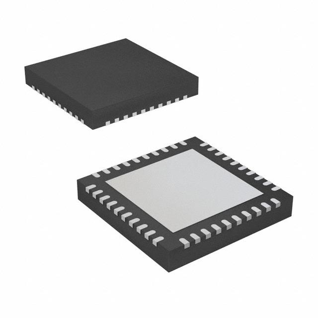


 工商网监
湘ICP备2023018690号
工商网监
湘ICP备2023018690号
