PRELIMINARY DATA SHEET
SKY87609: 28 V Step-Down DC-DC Controller with Optional
Synchronous MOSFET Driver
Applications
Description
• Set-top boxes
The SKY87609 is a step-down DC-DC controller that operates
over a wide 4.5 V to 28 V input voltage range and regulates output
voltage as low as 0.9 V while supplying up to 6 A to the output.
The 450 kHz switching frequency allows an efficient step-down
regulator design.
• LCD TV LED backlighting
• Industrial applications
Features
• 4.5 V to 28 V input voltage
• Controller with internal 10 Ω refresh MOSFET
• Up to 6 A load current
• Optional low-side MOSFET driver
• Adjustable output voltage (0.9 V to 0.8 × VIN)
• Fixed 450 kHz switching frequency
• 4 ms soft-start period
• External compensation
• Less than 1 µA shutdown current
• Up to 97% efficiency
The SKY87609 uses an adjustable output voltage that can be set
from 0.9 V to 80% of the input voltage by an external resistive
voltage divider. Internal soft-start prevents excessive inrush
current without requiring an external capacitor.
The SKY87609 includes input under-voltage and over-current
protection to prevent damage in the event of a fault. Thermal
overload protection prevents damage to the SKY87609 or circuit
board when operating beyond its thermal capability.
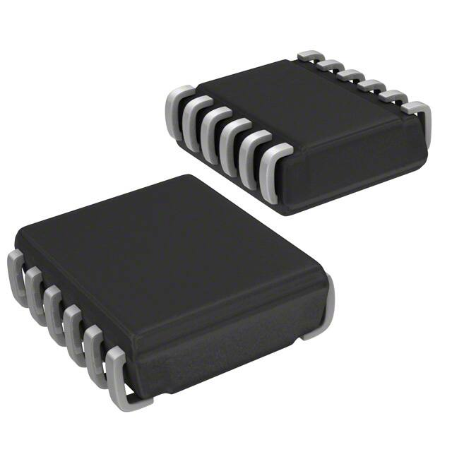
The SKY87609 is available in a small 12-pin
2.85 mm × 3.00 mm TSOPJW package.
A typical application circuit is shown in Figure 1. The pin
configuration is shown in Figure 2. Signal pin assignments and
functional pin descriptions are provided in Table 1.
• Current limit protection
• Compact TSOPJW (12-pin, 2.85 mm × 3.00 mm) package
(MSL1, 260 °C per JEDEC-J-STD-020)
Skyworks Solutions, Inc. • Phone [781] 376-3000 • Fax [781] 376-3100 • sales@skyworksinc.com • www.skyworksinc.com
201871B • Skyworks Proprietary Information • Products and Product Information are Subject to Change Without Notice • June 21, 2013
1
�PRELIMINARY DATA SHEET • SKY87609 28 V STEP-DOWN DC-DC CONTROLLER WITH OPTIONAL SYNCHRONOUS MOSFET DRIVER
Figure 1. SKY87609 Typical Application Circuit
Figure 2. SKY87609 12-Pin TSOPJW
(Top View)
Table 1. SKY87609 Signal Descriptions
Pin #
Name
Description
1
AGND
Analog ground. AGND is internally connected to the analog ground of the control circuitry.
2
PGND
Power ground. PGND is internally connected to the low-side driver and source of the 30 Ω refresh MOSFET.
DL
Low-side N-channel MOSFET driver output. For efficient designs, connect to the gate of the low-side N-channel MOSFET. DL switches
between VCC and PGND. For simple non-synchronous designs, leave DL unconnected.
LX
Inductor switching node. LX is internally connected to the high-side driver and current-sense circuitry. Connect to the source of the
high-side N-channel MOSFET, the power inductor, and the rectifier (diode or low-side MOSFET) as shown in Figure 1.
NC
Do not connect.
IN
Input supply. Connect IN to the input power source. Bypass IN to GND with a 10 µF or greater ceramic capacitor. IN externally connects
to the source of the high-side N-channel MOSFET and internally connects to the linear regulators powering the controller and drivers.
7
DH
High-side N-channel MOSFET driver output.
8
BST
Boot-strapped high-side driver supply. Connect a 0.1 µF ceramic capacitor between BST and LX as shown in Figure 1.
9
VCC
Driver bypass. VCC is the output of the linear regulator used to power the MOSFET drivers. For synchronous designs, connect a 0.1 µF
to 1 µF ceramic capacitor between VCC and PGND. For non-synchronous designs, the capacitor may be left open.
10
EN
Enable input. A logic high enables the controller. A logic low forces the SKY87609 into shutdown mode, placing the output into a highimpedance state and reducing the quiescent current to less than 1 µA.
11
COMP
Compensation pin of the error amplifier.
12
FB
Feedback input. FB senses the output voltage for regulation control. Connect a resistive divider network from the output to FB to GND
to set the output voltage accordingly. The FB regulation threshold is 0.9 V.
3
4
5
6
Skyworks Solutions, Inc. • Phone [781] 376-3000 • Fax [781] 376-3100 • sales@skyworksinc.com • www.skyworksinc.com
2
June 21, 2013 • Skyworks Proprietary Information • Products and Product Information are Subject to Change Without Notice • 201871B
�PRELIMINARY DATA SHEET • SKY87609 28 V STEP-DOWN DC-DC CONTROLLER WITH OPTIONAL SYNCHRONOUS MOSFET DRIVER
Electrical and Mechanical Specifications
The absolute maximum ratings of the SKY87609 are provided in
Table 2. Thermal information is provided in Table 3, and electrical
specifications are provided in Table 4.
Typical performance characteristics of the SKY87609 are
illustrated in Figures 3 through 35.
Table 2. SKY87609 Absolute Maximum Ratings (Note 1)
Parameter
Symbol
Minimum
Typical
Maximum
Units
–0.3
+30
V
IN to PGND
VIN
LX to PGND
VLX
–0.3
VIN + 0.3
V
BST to PGND
VBST
Vcc – 0.3
VIN + 6.0
V
Vcc to AGND
VCC
–0.3
7.5, or VIN + 0.3
V
DH to LX
VDH
–0.3
VBST + 0.3
V
EN to AGND
VEN
–0.3
+30
V
FB to AGND
VFB
–0.3
+6.0
V
COMP to AGND
VCOMP
–0.3
+6.0
V
DL to PGND
VDL
–0.3
VCC – 0.3
V
AGND to PGND
VGND
–0.3
+0.3
V
Note 1: Exposure to maximum rating conditions for extended periods may reduce device reliability. There is no damage to device with only one parameter set at the limit and all other
parameters set at or below their nominal value. Exceeding any of the limits listed may result in permanent damage to the device.
CAUTION: Although this device is designed to be as robust as possible, Electrostatic Discharge (ESD) can damage this device. This device
must be protected at all times from ESD. Static charges may easily produce potentials of several kilovolts on the human body
or equipment, which can discharge without detection. Industry-standard ESD precautions should be used at all times.
Table 3. SKY87609 Thermal Information (Note 1)
Parameter
Symbol
Minimum
Typical
Maximum
Units
+85
°C
+150
°C
Operating ambient temperature
TA
–40
Operating junction temperature
TJ
–40
Maximum soldering temperature (at leads, 10 seconds)
TLEAD
300
°C
Maximum junction-to-ambient thermal resistance
θJA
140
°C/W
Maximum power dissipation (Note 2)
PD
0.7
W
2
Note 1: Mounted on 1 in FR4 board.
Note 2: Derate 7 mW/°C above 25 °C.
Skyworks Solutions, Inc. • Phone [781] 376-3000 • Fax [781] 376-3100 • sales@skyworksinc.com • www.skyworksinc.com
201871B • Skyworks Proprietary Information • Products and Product Information are Subject to Change Without Notice • June 21, 2013
3
�PRELIMINARY DATA SHEET • SKY87609 28 V STEP-DOWN DC-DC CONTROLLER WITH OPTIONAL SYNCHRONOUS MOSFET DRIVER
Table 4. SKY87609 Electrical Specifications (Note 1)
(VIN = 12 V, VEN = 5 V, AGND = PGND, TA = -40 °C to 85 °C [Typical Values are at TA = 25 °C], Unless Otherwise Noted)
Parameter
Symbol
Test Condition
Input voltage
VIN
No load supply current
IQ
No load current; not switching
Shutdown current
ISHDN
EN = GND, VIN = 28 V
Output voltage (Note 2)
VOUT
Min
Typical
Max
28
V
1.6
3.2
mA
1
5
µA
0.8 × VIN
V
4.5
VFB
Nominal feedback voltage
0.9
V
FB accuracy
VFB
VIN = 24 V
0.88
FB leakage current
IFB
FB = 1.5 V or GND
–0.2
Load regulation
∆VOUT / IOUT
VIN = 12 V, Vout = 5 V
Line regulation
∆VOUT / VIN
VIN = 4.5 V to 28 V
Oscillator frequency
fOSC
0.92
V
+0.2
µA
Minimum on time
tON(MIN)
Maximum duty cycle
DMAX
No Load
80
83
%
Current limit voltage threshold
VCL(TH)
IN to LX
400
500
mV
Refresh MOSFET On resistance
RDS(ON)LO
VIN = 5 V
Input under-voltage lockout
VUVLO
VIN rising, hysteresis = 200 mV
Over-temperature shutdown threshold
TSHDN
Rising edge, hysteresis = 15 °C
EN input logic threshold
VEN
EN input current
IEN
Soft-start period
tSS
0.5
%
0.1
380
0.4 V, 12 V
0.90
%
450
520
kHz
370
540
ns
Ω
10
3.5
4.2
150
V
°C
0.4
1.7
V
–2.0
+25
µA
4
Note 1: Performance is guaranteed only under the conditions listed in this Table.
Note 2: The minimum output voltage must be greater than tON(MIN) × fOSC × VIN(MIN) due to duty cycle limitations.
Skyworks Solutions, Inc. • Phone [781] 376-3000 • Fax [781] 376-3100 • sales@skyworksinc.com • www.skyworksinc.com
4
Units
June 21, 2013 • Skyworks Proprietary Information • Products and Product Information are Subject to Change Without Notice • 201871B
ms
�PRELIMINARY DATA SHEET • SKY87609 28 V STEP-DOWN DC-DC CONTROLLER WITH OPTIONAL SYNCHRONOUS MOSFET DRIVER
Typical Performance Characteristics
Figure 3. Efficiency vs Output Current
(VOUT = 3.3 V)
Figure 4. Efficiency vs Output Current
(VOUT = 5.0 V)
Figure 5. Efficiency vs Output Current
(VOUT = 12 V)
Figure 6. Efficiency vs Output Current
(VOUT = 15 V)
Figure 7. Efficiency vs Output Current
(VOUT = 18 V)
Figure 8. Load Regulation vs Output Current
(VOUT = 3.3 V)
Skyworks Solutions, Inc. • Phone [781] 376-3000 • Fax [781] 376-3100 • sales@skyworksinc.com • www.skyworksinc.com
201871B • Skyworks Proprietary Information • Products and Product Information are Subject to Change Without Notice • June 21, 2013
5
�PRELIMINARY DATA SHEET • SKY87609 28 V STEP-DOWN DC-DC CONTROLLER WITH OPTIONAL SYNCHRONOUS MOSFET DRIVER
Typical Performance Characteristics
Figure 9. Load Regulation vs Output Current
(VOUT = 12 V)
Figure 10. Load Regulation vs Output Current
(VOUT = 15 V)
Figure 11. Load Regulation vs Output Current
(VOUT = 18 V)
Figure 12. Line Regulation vs Input Voltage
(VOUT = 3.3 V)
Figure 13. Line Regulation vs Input Voltage
(VOUT = 12 V)
Figure 14. Line Regulation vs Input Voltage
(VOUT = 15 V)
Skyworks Solutions, Inc. • Phone [781] 376-3000 • Fax [781] 376-3100 • sales@skyworksinc.com • www.skyworksinc.com
6
June 21, 2013 • Skyworks Proprietary Information • Products and Product Information are Subject to Change Without Notice • 201871B
�PRELIMINARY DATA SHEET • SKY87609 28 V STEP-DOWN DC-DC CONTROLLER WITH OPTIONAL SYNCHRONOUS MOSFET DRIVER
Typical Performance Characteristics
Figure 15. Line Regulation vs Input Voltage
(VOUT = 18 V)
Figure 16. Oscillator Frequency vs Temperature
(IOUT = 100 mA)
Figure 17. Soft Start
(VOUT = 5 V, VIN = 12 V, IOUT = 0 A)
Figure 18. Soft Start
(VOUT = 5 V, VIN = 12 V, IOUT = 5 A)
Figure 19. Soft Start
(VOUT = 5 V, VIN = 24 V, IOUT = 0 A)
Figure 20. Soft Start
(VOUT = 5 V, VIN = 24 V, IOUT = 6 A)
Skyworks Solutions, Inc. • Phone [781] 376-3000 • Fax [781] 376-3100 • sales@skyworksinc.com • www.skyworksinc.com
201871B • Skyworks Proprietary Information • Products and Product Information are Subject to Change Without Notice • June 21, 2013
7
�PRELIMINARY DATA SHEET • SKY87609 28 V STEP-DOWN DC-DC CONTROLLER WITH OPTIONAL SYNCHRONOUS MOSFET DRIVER
Typical Performance Characteristics
Figure 21. Output Voltage Ripple
(VOUT = 5 V, VIN = 12 V, IOUT = 100 mA)
Figure 22. Output Voltage Ripple
(VOUT = 5 V, VIN = 12 V, IOUT = 6 A)
Figure 23. Output Voltage Ripple
(VOUT = 5 V, VIN = 24 V, IOUT = 100 mA)
Figure 24. Output Voltage Ripple
(VOUT = 5 V, VIN = 24 V, IOUT = 6 A)
Figure 25. Output Voltage Ripple
(VOUT = 12 V, VIN = 24 V, IOUT = 100 mA)
Figure 26. Output Voltage Ripple
(VOUT = 12 V, VIN = 24 V, IOUT = 6 A)
Skyworks Solutions, Inc. • Phone [781] 376-3000 • Fax [781] 376-3100 • sales@skyworksinc.com • www.skyworksinc.com
8
June 21, 2013 • Skyworks Proprietary Information • Products and Product Information are Subject to Change Without Notice • 201871B
�PRELIMINARY DATA SHEET • SKY87609 28 V STEP-DOWN DC-DC CONTROLLER WITH OPTIONAL SYNCHRONOUS MOSFET DRIVER
Typical Performance Characteristics
Figure 27. Output Voltage Ripple
(VOUT = 15 V, VIN = 24 V, IOUT = 100 mA)
Figure 28. Output Voltage Ripple
(VOUT = 15 V, VIN = 24 V, IOUT = 6 A)
Figure 29. Output Voltage Ripple
(VOUT = 18 V, VIN = 24 V, IOUT = 100 mA)
Figure 30. Output Voltage Ripple
(VOUT = 18 V, VIN = 24 V, IOUT = 6 A)
Figure 31. Load Transient
(VOUT = 5 V, VIN = 12 V, IOUT = 0.1 to 6 A)
Figure 32. Load Transient
(VOUT = 5 V, VIN = 24 V, IOUT = 0.1 to 6 A)
Skyworks Solutions, Inc. • Phone [781] 376-3000 • Fax [781] 376-3100 • sales@skyworksinc.com • www.skyworksinc.com
201871B • Skyworks Proprietary Information • Products and Product Information are Subject to Change Without Notice • June 21, 2013
9
�PRELIMINARY DATA SHEET • SKY87609 28 V STEP-DOWN DC-DC CONTROLLER WITH OPTIONAL SYNCHRONOUS MOSFET DRIVER
Typical Performance Characteristics
Figure 33. Load Transient
(VOUT = 12 V, VIN = 24 V, IOUT = 0.1 to 6 A)
Figure 34. Load Transient
(VOUT = 15 V, VIN = 24 V, IOUT = 0.1 to 6 A)
Figure 35. Load Transient
(VOUT = 18 V, VIN = 24 V, IOUT = 0.1 to 6 A)
Skyworks Solutions, Inc. • Phone [781] 376-3000 • Fax [781] 376-3100 • sales@skyworksinc.com • www.skyworksinc.com
10
June 21, 2013 • Skyworks Proprietary Information • Products and Product Information are Subject to Change Without Notice • 201871B
�PRELIMINARY DATA SHEET • SKY87609 28 V STEP-DOWN DC-DC CONTROLLER WITH OPTIONAL SYNCHRONOUS MOSFET DRIVER
Figure 36. SKY87609 Functional Block Diagram
Functional Description
Voltage Soft-Start
A functional block diagram is provided in Figure 36.
The soft-start circuit ramps the reference voltage from ground up
to the 0.9 V nominal feedback regulation voltage (see the
functional block diagram in Figure 36). The internal soft-start
capacitor sets the soft-start period as 4 ms (typical).
Control Scheme
The SKY87609 is a constant frequency, current-mode step-down
controller. The controller has a low-side MOSFET driver and an
internal 10 Ω boost capacitor refresh MOSFET that allows both
synchronous and non-synchronous designs. A floating gate driver
powers the high-side N-channel MOSFET from an external bootstrap capacitor through the BST pin. The capacitor is charged
when LX is pulled low through an external rectifier, and the BST
capacitor maintains sufficient voltage to enhance the high-side Nchannel MOSFET during the on time.
The SKY87609 supports an adjustable output voltage using an
external resistive voltage divider, allowing the output to be set to
any voltage between 0.9 V and 80% of the input voltage. The
SKY87609 switches at 450 kHz.
Current Limit Protection
The SKY87609 includes protection for overload and short-circuit
conditions by limiting the peak inductor current. During the on
time, the controller monitors the current through the high-side
MOSFET (IN to LX voltage). If the voltage drop across the MOSFET
exceeds 500 mV (typical), the regulator immediately turns off the
high-side MOSFET.
The soft-start is discharged/reset if any of the following events
occurs: the controller is disabled (EN is pulled low), the input
voltage drops below the Under-Voltage Lockout (UVLO) threshold,
or the thermal shutdown is activated.
Thermal Shutdown
The SKY87609 includes thermal protection that disables the
controller when the die temperature reaches 150 °C. The thermal
shutdown resets the soft-start circuit and automatically restarts
when the temperature drops below 135 °C.
Application Information
To ensure that the maximum possible performance is obtained
from the SKY87609, refer to the following application
recommendations for component selection.
Skyworks Solutions, Inc. • Phone [781] 376-3000 • Fax [781] 376-3100 • sales@skyworksinc.com • www.skyworksinc.com
201871B • Skyworks Proprietary Information • Products and Product Information are Subject to Change Without Notice • June 21, 2013
11
�PRELIMINARY DATA SHEET • SKY87609 28 V STEP-DOWN DC-DC CONTROLLER WITH OPTIONAL SYNCHRONOUS MOSFET DRIVER
Design Methodology
Setting the Output Voltage
This section details the component selection process for the
SKY87609 in continuous conduction mode to assist with the
design process. Many of the equations make heavy use of the
small ripple approximation. This process includes the following
steps:
The SKY87609 output voltage is adjustable from 0.9 V up to 80%
of VIN by connecting FB to the center tap of a resistor-divider
between the output and GND (see Figure 37). The resistive
feedback voltage divider sets the output voltage according to the
following relationship:
1. Operational parameters definition
V
RFB1 = OUT − 1 × RFB 2
0.9V
2. Output voltage setting
3. Inductor selection
which is rounded to the nearest 1% resistor value. RFB2 is
typically selected to be between 10 kΩ and 200 kΩ. The lower
resistance value improves the noise immunity, but results in
higher feedback current (reducing the efficiency).
4. Output capacitor selection
5. Input capacitor selection
6. Peak current limit setting
7. N-channel MOSFET(s) selection
8. Rectifying Schottky diode selection
9. Stability and compensation components selection
10. Bootstrap capacitor selection
11. Thermal consideration
Define Operational Parameters
Before starting the design, define the operating parameters of the
application. These parameters include:
VIN(MIN): minimum input voltage, in Volts
VIN(MAX): maximum input voltage, in Volts
VOUT: output voltage, in Volts
IOUT(MAX): maximum output current, in Amps
ICL: desired typical cycle-by-cycle current limit, in Amps
Figure 37. FB Resistor Divider
Table 5 shows the divider resistor value for different output
voltages.
Using the equation below:
VOUT = D × VIN
where D is the duty cycle, the minimum and maximum
duty cycles can be closely approximated by the following
equations:
D( MIN )
V
= OUT
VIN ( MAX )
D( MAX )
V
= OUT
VIN ( MIN )
Both the minimum and maximum duty cycles actually are higher
due to power losses in the conversion. The exact duty cycle
depends on conduction and switching losses. The SKY87609 has
a typical maximum duty cycle of 90%. If the maximum duty cycle
is exceeded due to a low VIN(MIN) voltage, VOUT is out of
regulation, and can be determined by the following equation:
Table 5. Resistor Selection for Different Output Voltages
Output Voltage (V)
RFB1 (kΩ)
(RFB2 = 20 kΩ)
1.5
13.3
3.3
53.6
5.0
91.0
8.0
158.0
10.0
200.0
12.0
249.0
15.0
316.0
18.0
383.0
20.0
422.0
VOUT = DMAX × VIN ( MIN )
where DMAX = the maximum duty cycle of the SKY87609
(83% typical).
Skyworks Solutions, Inc. • Phone [781] 376-3000 • Fax [781] 376-3100 • sales@skyworksinc.com • www.skyworksinc.com
12
June 21, 2013 • Skyworks Proprietary Information • Products and Product Information are Subject to Change Without Notice • 201871B
�PRELIMINARY DATA SHEET • SKY87609 28 V STEP-DOWN DC-DC CONTROLLER WITH OPTIONAL SYNCHRONOUS MOSFET DRIVER
Inductor Selection
characteristics. The inductor should not show any appreciable
saturation under normal load conditions.
The step-down converter uses peak current mode control with
slope compensation to maintain stability for duty cycles greater
than 50%. The output inductor value must be selected to make
the inductor current down slope meet the internal slope
compensation requirements. The internal slope compensation is
designed to be 75% of the inductor current down slope of 5 V
output with a 6.8 µH inductor.
mC =
The saturation current is a very important parameter for inductor
selection. It must be more than the sum of DC current and
maximum peak current through the inductor, and the adequate
margin is important for safe application. The maximum peak
current is given by the equation below.
0.75 × VOUT 0.75 × 5V
=
L
0.68 µH
I PEAK_INDUCTOR_MAX
where L is the inductance, and f is the operation frequency.
A
mC = 0.55 ×
µs
Some inductors that meet the peak and average current ratings
requirements still result in excessive losses due to a high Direct
Current Resistance (DCR). Always consider the losses associated
with the DCR and their effect on the total regulator efficiency
when selecting an inductor.
For other output voltages, the inductance can be calculated based
on the internal slope compensation requirement and equal to:
L=
V
VOUT × 1 − OUT
V
IN ( MAX )
=
L× f
0.75 × VOUT
= (1.36 × VOUT )(µH )
mC
Table 6 shows the recommended inductors for different output
voltages.
Manufacturer specifications list both the inductor DC current
rating, which is dependent on the thermal limitation, and the peak
current rating, which is determined by the saturation
Table 6. Inductor Selection for Different Output Voltages (1 of 2)
Vout
(V)
Inductance
(µH)
2.5
1.5
3.3
5
10
12
2.2
4.7
6.8
15
18
Saturation Current
(A)
DCR
(mΩ)
CDRH8D38NP-2R5N
5.5
17.5
8.3×8.3×4
744777002
6.5
20
7.3×7.3×4.5
Wurth Elektronik
DR73-2R2-R
5.52
16.5
7.9×7.9×3.8
Coil Tronics
CDRH105RNP-4R7N
6.4
12.3
10.5×10.3×5.1
CDRH10D68NP-4R7N
6.6
9.8
10.5×10.5×7.1
Part Number
Dimensions
L×W×H (mm)
7447715004
6.3
16
12×12×4.5
CDRH105RNP-6R8N
5.4
18
10.5×10.3×5.1
CDRH124NP-6R8M
4.9
23
12.3×12.3×4.5
7447715006
4.7
25
12×12×4.5
CDRH127NP-15M
4.5
27
12.3×12.3×8
CDRH127/LDHF-150M
5.65
26.4
12.3×12.3×8
744771115
4.55
30
12×12×6
DR125-150-R
5.69
29.8
13×13×6.3
CDRH127/LDHF-180M
5.1
28
12.3×12.3×8
744771118
4.3
34
12×12×6
DR125-180-R
5.32
37.7
13×13×6.3
Manufacturer
Sumida
Sumida
Wurth Elektronik
Sumida
Wurth Elektronik
Sumida
Wurth Elektronik
Coil Tronics
Sumida
Wurth Elektronik
Coil Tronics
Skyworks Solutions, Inc. • Phone [781] 376-3000 • Fax [781] 376-3100 • sales@skyworksinc.com • www.skyworksinc.com
201871B • Skyworks Proprietary Information • Products and Product Information are Subject to Change Without Notice • June 21, 2013
13
�PRELIMINARY DATA SHEET • SKY87609 28 V STEP-DOWN DC-DC CONTROLLER WITH OPTIONAL SYNCHRONOUS MOSFET DRIVER
Table 6. Inductor Selection for Different Output Voltages (2 of 2)
Vout
(V)
15
18
20
Inductance
(µH)
22
27
27
Saturation Current
(A)
D.C.R
(mΩ)
Dimension(mm)
L×W×H
CDRH127/LDHF-220M
4.7
36.4
12.3×12.3×8
744770122
5.0
43
12×12×8
DR125-220-R
4.71
39.6
13×13×6.3
CDRH127/LDHF-270M
4.2
41.6
12.3×12.3×8
744770127
3.8
46
12×12×8
7447709270
5.8
40
12×12×10
CDRH127/LDHF-270M
4.2
41.6
12.3×12.3×8
744770127
3.8
46
12×12×8
7447709270
5.8
40
12×12×10
Part Number
Output Capacitor Selection
The output capacitor impacts stability, limits the output ripple
voltage, and maintains the output voltage during large load
transitions. The SKY87609 is designed to work with any type of
output capacitor since the controller features externally adjustable
compensation (see the "Stability Considerations" and
"Compensation Component Selection" sections of this Data
Sheet).
The key capacitor parameters for selecting the output capacitors
are capacitance, Equivalent Series Resistance (ESR), (Effective
Series Inductance (ESL) and voltage ratings. The output ripple
occurs due to variations in the charge stored in the output
capacitor, the voltage drop due to the capacitor’s ESR, and the
voltage drop due to the capacitor’s ESL. Estimate the output
voltage ripple due to the output capacitance, ESR, and ESL as
follows:
VOUT ( RIPPLE ) = VRIPPLE ( C ) + VRIPPLE ( ESR ) + VRIPPLE ( ESL )
where the output ripple due to output capacitance, ESR, and ESL
is:
VRIPPLE ( C ) =
∆I L
8 × COUT × f SW
VRIPPLE ( ESR ) = ∆I L × ESR
VRIPPLE ( ESL ) = VLX ×
ESL
ESL
= VIN ×
L
L
The peak-to-peak inductor current ΔIL is:
(V
∆I L =
IN ( MAX )
− VOUT ) ×
Manufacturer
Sumida
Wurth Elektronik
Coil Tronics
Sumida
Wurth Elektronik
Sumida
Wurth Elektronik
electrolytic capacitors, VRIPPLE(ESR) dominates. Use ceramic
capacitors for low ESR and low ESL at the switching frequency of
the converter. The ripple voltage due to ESL is negligible when
using ceramic capacitors.
After a load step occurs, the output capacitor must support
the difference between the load requirement and inductor current.
Once the average inductor current increases to the DC load level,
the output voltage recovers. Therefore, based on limitations in the
ability to discharge the inductor, a minimum output voltage
deviation may be determined by the following:
VSOAR (C ) =
2
∆I OUT
×L
2 × COUT × VOUT
VSOAR ( ESR ) = ∆I OUT × ESR
where VSOAR is the output voltage overshoot and undershoot
deviation. Bandwidth and gain limitations (dependent on output
capacitor and compensation component selection) may result in
larger output voltage deviations.
The ceramic output capacitor provides low ESR and low ESL,
resulting in low output ripple dominated by capacitive ripple
voltage (ΔVOUT(c)). However, due to the lower capacitance value,
the load transient response is significantly worse. Therefore,
ceramic output capacitors are generally recommended only for
designs with soft load transients (slow di/dt and/or small load
steps).
Tantalum and electrolytic capacitors can provide a highcapacitance, low-cost solution. The bulk capacitance provides
minimal output voltage drop/soar after load transients occur.
VOUT
VIN ( MAX )
L × f SW
The capacitive ripple and ESR ripple are phase shifted from each
other, but depending on the type of output capacitor chemistry,
one of them typically dominates. When using ceramic capacitors,
which generally have low ESR, VRIPPLE(c) dominates. When using
Skyworks Solutions, Inc. • Phone [781] 376-3000 • Fax [781] 376-3100 • sales@skyworksinc.com • www.skyworksinc.com
14
June 21, 2013 • Skyworks Proprietary Information • Products and Product Information are Subject to Change Without Notice • 201871B
�PRELIMINARY DATA SHEET • SKY87609 28 V STEP-DOWN DC-DC CONTROLLER WITH OPTIONAL SYNCHRONOUS MOSFET DRIVER
Input Capacitor Selection
Typically, the input impedance is so low (or other input capacitors
are distributed throughout the system) that a single 10 μF, X7R, or
X5R ceramic capacitor located near the SKY87609 is sufficient.
However, additional input capacitance may be necessary
depending on the impedance of the input supply. To estimate the
required input capacitance requirement, determine the acceptable
input ripple level (VPP) and solve CIN:
C IN
VOUT VOUT
× 1 −
VIN
VIN
D × (1 − D )
=
=
VPP
V
− ESR × f SW PP − ESR × f SW
I
I
OUT
OUT
Always examine the ceramic capacitor DC voltage coefficient
characteristics when evaluating ceramic bypass capacitors.
In addition to the capacitance requirement, the RMS current
rating of the input capacitor must be able to support the pulsed
current drawn by the step-down regulator. The input RMS current
requirement may be determined by:
I RMS = I OUT ×
VOUT VOUT
× 1 −
VIN
VIN
= I OUT × D × (1 − D )
The term D × (1 – D) appears in both the input ripple voltage and
input capacitor RMS current equations, so the maximum occurs
when VOUT = 0.5 × VIN (50% duty cycle). This results in a set of
“worst case” capacitance and RMS current design requirements:
C IN ( MIN ) =
1
V
4 × PP − ESR × f SW
I
OUT
I RMS ( MAX ) =
I OUT
2
The input capacitor provides a low impedance loop for the pulsed
current drawn by the SKY87609. Low ESR/ESL X7R and X5R
ceramic capacitors are ideal for this function. To minimize the
stray inductance, the capacitor should be placed as closely as
possible to the high-side MOSFET. This keeps the high-frequency
content of the input current localized, minimizing EMI and input
voltage ripple. The proper placement of the input capacitor can be
seen in the Evaluation Board layout.
In applications where the lead inductance of the input power
source cannot be reduced to a level that does not affect the
regulator performance, a high-ESR tantalum or aluminum
electrolytic should be placed in parallel with the low ESR/ESL
ceramic capacitor. This reduces the input impedance and
dampens the high-Q network, stabilizing the input supply.
That voltage is compared with the 500 mV (reference) voltage of
the CS comparator. When the voltage drop across the MOSFET
exceeds 500 mV (typical), the regulator immediately turns off the
high-side MOSFET for the duration of the switching cycle.
Calculating the current limit:
I PCL =
VCLTH
RDS ( ON )
where VCLTH = 500 mV.
Be sure that the rated peak current of the MOSFET is greater than
the set current limit.
N-Channel MOSFET(s) Selection
High-Side Switching MOSFET
The following key parameters must be met by the selected
MOSFET:
• Drain-source voltage, VDS, must be able to withstand the input
voltage plus overshoots that may be on the switching node. For
a VIN of 12 V, a VDS rating of 25 to 30 V is recommended.
• Drain current, ID, at 25°C must be greater than the calculated
switching current:
ID =
2
VOUT
∆I 2
× I LOAD
+
( MAX )
VIN ( MIN )
12
• Gate-source voltage, VGS, must be greater than Vin.
Once the above boundary parameters are defined, the next step in
selecting the high-side switching MOSFET is to select the key
performance parameters. Efficiency is the performance
characteristic that drives the other selections criteria. Based on
the target efficiency, the power losses in the converter can be
calculated as:
I D = (1 − ηTARGET ) × (VOUT × I LOAD )
For example, if the target efficiency is 90% for a 5 V output and
5 A load, then the power loss in the converter is:
(1 − 0.90) × (5 V × 5 A) = 2.5 W
Typically, 20% of the power loss in the converter is used as the
power dissipated in the switching MOSFET.
The following equations can be used to calculate the power
losses, PHSFET, in the high-side switching MOSFET.
PHSFET = PHSFET(CON) + PHSFET(SW) + PHSFET(GATE)
PHSFET(CON) =
VOUT 2
∆I 2
× I LOAD +
VIN
12
Setting the Peak Current Limit
The SKY87609 uses the RDS(ON) of the high-side MOSFET to
convert the on-time inductor current to a proportional voltage.
Skyworks Solutions, Inc. • Phone [781] 376-3000 • Fax [781] 376-3100 • sales@skyworksinc.com • www.skyworksinc.com
201871B • Skyworks Proprietary Information • Products and Product Information are Subject to Change Without Notice • June 21, 2013
15
�PRELIMINARY DATA SHEET • SKY87609 28 V STEP-DOWN DC-DC CONTROLLER WITH OPTIONAL SYNCHRONOUS MOSFET DRIVER
PHSFET(SW) = V IN × f SW
2
∆I 2
× (Q GS 1 + Q GD )
I LOAD +
QOSS ( HSFET ) + QOSS ( LSFET )
12
×
+
IG
2
PHSFET(GATE) = QG(TOT) × VG × f SW
where:
PHSFET(CON) = conduction losses
PHSFET(SW) = switching losses
PHSFET(GATE) = gate drive losses
QGD = drain-source charge or Miller charge
QGS1 = gate-source post threshold charge
IG = gate drive current
QOSS(HSFET) = high-side switching MOSFET output charge
QOSS(LSFET) = low-side synchronous MOSFET output charge
QG(TOT) = total gate charge from 0 V to gate voltage
VG = gate voltage
It is not always possible to get a MOSFET that meets both of these
criteria, so a compromise may have to be made. Also, by
selecting different MOSFETs close to this criteria and calculating
power losses, the final selection can be made.
Low-Side synchronous MOSFET
Similar criteria can be used for the rectifier MOSFET, with one
significant difference. The body diode is conducting, so the
rectifier MOSFET switches with near zero voltage across its drain
and source, and the switching losses are near zero. However,
there are some losses in the body diode. These are minimized by
reducing the delay time between the transition from the switching
MOSFET turn-off to rectifier MOSFET turn-on and vice versa.
The following equations can be used to calculate the power loss,
PLSFET, in the low-side synchronous MOSFET:
PLSFET = PLSFET(CON) + PLSFET(DIODE) + PHSFET(GATE)
PLSFET(CON) = RDS ( ON ) ×
VOUT 2
∆I 2
× I LOAD +
VIN
12
PLSFET(DIODE) = VF × I LOAD × (t1 + t 2 ) × f SW
Rectifying Schottky Diode Selection
Power dissipation is the limiting factor when choosing a diode.
The worst-case average power can be calculated as follows:
V
PDIODE = 1 − OUT × I OUT ( MAX ) × VDIODE
V
IN (MAX)
where VDIODE is the voltage drop across the diode at the given
output current IOUT(MAX). (Typical values are 0.7 V for a silicon
diode and 0.3 V for a Schottky diode.) Ensure that the selected
diode is able to dissipate that much power. For reliable operation
over the input voltage range, also ensure that the reverse
repetitive maximum voltage is greater than the maximum input
voltage (VRRM ≥ VIN(MAX)). The diode's forward current
specification must meet or exceed the maximum output current
(i.e., IFAX ≥ IOUT(MAX)).
Stability Considerations
The SKY87609 uses a current-mode architecture that relies on
the output capacitor and a series resistor-capacitor network on
the COMP pin for stability. COMP is the output of the
transconductance error amplifier, so the RC network creates a
pole-zero pair used to control the gain and bandwidth of the
control loop.
The DC loop gain (ADC) is set by the voltage gain of the internal
transconductance amplifier (AEA = gm(EA) × ROUT = 500 V/V), the
compensation gain (ACC = 400 mV/V), and the current-sense gain
(ACS = 1 V/V):
ADC =
where VFB is the 0.9 V feedback voltage, VOUT is the output
voltage determined by the feedback resistors, RDS(ON) is the onresistance of the high-side N-channel MOSFET, and RLOAD is the
output load resistance (RLOAD = VOUT /IOUT). Since the output
impedance is a function of the load current and output voltage,
the equation may be rewritten independent of the VOUT term:
ADC =
PLSFET(GATE) = QG(TOT) × VG × f SW
where,
PLSFET(DIODE) = body diode losses
t1 = body diode conduction prior to the turn on of channel
t2 = body diode conduction after the turn off of channel
VF = body diode forward voltage
ACC
VFB
×
× AEA × RLOAD
VOUT ACS × RDS ( ON )
ACC
VFB
×
× AEA
I OUT ACS × RDS ( ON )
Additionally, the high-side on-resistance RDS(ON) is inversely
proportional to the maximum output current (IOUT) due to the peak
current limit. This effectively limits the typical value of ADC to a
value of 360 V/V (51 dB).
The control loop has two dominant poles: one created by the
output capacitor (COUT) and load resistance, and the other formed
by the total compensation capacitance (CCC1 + CCC2) and the
error amplifier transconductance (gm(EA) = 500 μA/V):
f P1 =
I OUT
1
=
2π × RLOAD × COUT 2π × VOUT × COUT
Skyworks Solutions, Inc. • Phone [781] 376-3000 • Fax [781] 376-3100 • sales@skyworksinc.com • www.skyworksinc.com
16
June 21, 2013 • Skyworks Proprietary Information • Products and Product Information are Subject to Change Without Notice • 201871B
�PRELIMINARY DATA SHEET • SKY87609 28 V STEP-DOWN DC-DC CONTROLLER WITH OPTIONAL SYNCHRONOUS MOSFET DRIVER
f P2 =
gm( EA )
2π × AEA × (CCC 1 + CCC 2 )
However, the system also has two zeros in the control loop: one
created by the series compensation resistor (RCOMP) and capacitor
(CCC1), and the other formed by the output capacitor and its
parasitic series resistance (ESR):
f Z1 =
f Z2
1
2π × RCOMP × CCC 1
1
=
2π × ESR × COUT
The ESR zero is highly dependent on the type of output capacitors
being used (ceramic vs tantalum), and may not occur before
crossover. If the ESR zero occurs low enough, the compensation
zero formed by RCOMP may be placed at crossover to avoid
stability problems.
However, if both zeros are required below crossover, a third pole
is needed to maintain stability. This third pole can be added by
including another compensation capacitor (CCC2 in Figure 38) in
parallel with the main series RC network:
f P3 =
1
CCC 1 × CCC 2
2π × RCOMP ×
CCC 1 + CCC 2
If CCC2


 工商网监
湘ICP备2023018690号
工商网监
湘ICP备2023018690号
