2 N1893
GENERAL PURPOSE HIGH-VOLTAGE TYPE
DESCRIPTION The 2N1893 is a silicon planar epitaxial NPN transistor in Jedec TO-39 metal case, designed for use in high-performance amplifier, oscillator and switching circuits. It provides greater voltage swings in oscillator and amplifier circuits and more protection in inductive switching circuits due to its 120 V collector-to-base voltage rating. Products approved to CECC 50002-104 available on request.
TO-39
INTERNAL SCHEMATIC DIAGRAM
ABSOLUTE MAXIMUM RATINGS
Symbol V CBO V CER V CEO V EBO IC Pt o t Parameter Collector-base Voltage (I E = 0) Collector-emitter Voltage (R BE ≤ 10 Ω ) Collector-emitter Voltage (I B = 0) Emitter-base Voltage (I C = 0) Collector Current Total Power Dissipation at T amb ≤ 25 °C at T c as e ≤ 25 °C at T c as e ≤ 100 °C Storage and Junction Temperature Value 120 100 80 7 0.5 0.8 3 1.7 – 65 to 200 Unit V V V V A W W W °C 1/5
T s t g, T j October 1988
�2N1893
THERMAL DATA
R t h j- cas e R t h j-amb Thermal Resistance Junction-case Thermal Resistance Junction-ambient Max Max 58 219 °C/W °C/W
ELECTRICAL CHARACTERISTICS (T amb = 25 °C unless otherwise specified)
Symbol I CBO I E BO V ( BR)
CBO
Parameter Collector Cutoff Current (I E = 0) Emitter Cutoff Current (I C = 0) Collector-base Breakdown Voltage (I E = 0) Collector-emitter Breakdown Voltage (R BE ≤ 10 Ω ) Collector-emitter Breakdown Voltage (I B = 0) Emitter-base Breakdown Voltage (I C = 0) Collector-emitter Saturation Voltage Base-emitter Saturation Voltage DC Current Gain
Test Conditions V CB = 90 V V CB = 90 V VE B = 5 V I C = 100 µA I C = 10 mA I C = 10 mA I E = 100 µA I C = 50 mA I C = 150 mA I C = 50 mA I C = 150 mA I C = 0.1 mA I C = 10 mA I C = 150 mA I C = 10 mA T amb = – 55 °C I C = 1 mA f = 1 kHz I C = 5 mA f = 1 kHz I C = 50 mA f = 20 MHz IC = 0 f = 1 MHz IE = 0 f = 1 MHz I B = 5 mA I B = 15 mA I B = 5 mA I B = 15 mA V CE V CE V CE V CE = = = = 10 10 10 10 V V V V T am b = 150 °C
Min.
Typ.
Max. 10 15 10
Unit nA µA nA V V V V
120 100 80 7 1.2 5 0.82 0.96 20 35 40 20 V CE = 5 V 30 V CE = 10 V 45 V CE = 10 V V EB = 0.5 V V CB = 10 V 50 85 70 55 13 85 15 70 150 50 80 80 40 0.9 1.3
V (BR)CE R * V (B R)CEO V ( BR) V CE V BE
EBO
(s at )*
V V V V
(s at )
*
h F E*
120
hfe
Small Signal Current Gain
fT C EBO C CBO
Transition Frequency Emitter-base Capacitance Collector-base Capacitance
MHz pF pF
* Pulsed : pulse duration = 300 µs, duty cycle = 1 %.
2/5
�2N1893
DC Current Gain. High-frequency Current Gain.
3/5
�2N1893
TO39 MECHANICAL DATA
mm DIM. MIN. A B D E F G H I L 5.08 1.2 0.9 45o (typ.) 12.7 0.49 6.6 8.5 9.4 0.200 0.047 0.035 TYP. MAX. MIN. 0.500 0.019 0.260 0.334 0.370 TYP. MAX. inch
D G I H E F
A
L B
P008B
4/5
�2N1893
Information furnished is believed to be accurate and reliable. However, SGS-THOMSON Microelectronics assumes no responsability for the consequences of use of such information nor for any infringement of patents or other rights of third parties which may results from its use. No license is granted by implication or otherwise under any patent or patent rights of SGS-THOMSON Microelectronics. Specifications mentioned in this publication are subject to change without notice. This publication supersedes and replaces all information previously supplied. SGS-THOMSON Microelectronics products are not authorized for use as critical components in life support devices or systems without express written approval of SGS-THOMSON Microelectonics. © 1994 SGS-THOMSON Microelectronics - All Rights Reserved SGS-THOMSON Microelectronics GROUP OF COMPANIES Australia - Brazil - France - Germany - Hong Kong - Italy - Japan - Korea - Malaysia - Malta - Morocco - The Netherlands Singapore - Spain - Sweden - Switzerland - Taiwan - Thailand - United Kingdom - U.S.A
5/5
�
很抱歉,暂时无法提供与“2N1893”相匹配的价格&库存,您可以联系我们找货
免费人工找货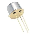


 工商网监
湘ICP备2023018690号
工商网监
湘ICP备2023018690号
