74AC373
OCTAL D-TYPE LATCH WITH 3 STATE OUTPUTS (NON INVERTED)
s s
s
s
s
s
s
s
s
HIGH SPEED: tPD = 5ns (TYP.) at VCC = 5V LOW POWER DISSIPATION: ICC = 4µA(MAX.) at TA=25°C HIGH NOISE IMMUNITY: VNIH = V NIL = 28 % VCC (MIN.) 50Ω TRANSMISSION LINE DRIVING CAPABILITY SYMMETRICAL OUTPUT IMPEDANCE: |IOH| = IOL = 24mA (MIN) BALANCED PROPAGATION DELAYS: tPLH ≅ tPHL OPERATING VOLTAGE RANGE: VCC (OPR) = 2V to 6V PIN AND FUNCTION COMPATIBLE WITH 74 SERIES 373 IMPROVED LATCH-UP IMMUNITY
DIP
SOP
TSSOP
ORDER CODES
PACKAGE DIP SOP TSSOP TUBE 74AC373B 74AC373M T&R 74AC373MTR 74AC373TTR
DESCRIPTION The 74AC373 is a high-speed CMOS OCTAL D-TYPE LATCH with 3 STATE OUTPUT NON INVERTING fabricated with sub-micron silicon gate and double-layer metal wiring C2MOS technology. These 8 bit D-Type latch are controlled by a latch enable input (LE) and an output enable input (OE). While the LE inputs is held at a high level, the Q outputs will follow the data input. When the LE is taken low, the Q outputs will be latched at the PIN CONNECTION AND IEC LOGIC SYMBOLS
logic level of D input data. While the (OE) input is low, the 8 outputs will be in a normal logic state (high or low logic level); while OE is in high level the outputs will be in a high impedance state. This device is designed to interface directly High Speed CMOS systems with TTL and NMOS components. All inputs and outputs are equipped with protection circuits against static discharge, giving them 2KV ESD immunity and transient excess voltage.
April 2001
1/11
�74AC373
INPUT AND OUTPUT EQUIVALENT CIRCUIT PIN DESCRIPTION
PIN No 1 2, 5, 6, 9, 12, 15, 16,19 3, 4, 7, 8, 13, 14, 17, 18 11 10 20 SYMBOL OE Q0 to Q7 D0 to D7 LE GND VCC NAME AND FUNCTION 3 State Output Enable Input (Active LOW) Data Inputs 3-State Outputs Latch Enable Input Ground (0V) Positive Supply Voltage
TRUTH TABLE
INPUTS OE H L L L LE X L H H D X X L H OUTPUT Q Z NO CHANGE L H
X : Don’t Care Z : High Impedance NOTE: Outputs are latched at the time when the input is taken LOW logic level
LOGIC DIAGRAM
This logic diagram has not be used to estimate propagation delays
2/11
�74AC373
ABSOLUTE MAXIMUM RATINGS
Symbol VCC VI VO IIK IOK IO Tstg TL Supply Voltage DC Input Voltage DC Output Voltage DC Input Diode Current DC Output Diode Current DC Output Current Storage Temperature Lead Temperature (10 sec) Parameter Value -0.5 to +7 -0.5 to VCC + 0.5 -0.5 to VCC + 0.5 ± 20 ± 20 ± 50 ± 400 -65 to +150 300 Unit V V V mA mA mA mA °C °C
ICC or IGND DC VCC or Ground Current
Absolute Maximum Ratings are those values beyond which damage to the device may occur. Functional operation under these conditions is not implied.
RECOMMENDED OPERATING CONDITIONS
Symbol VCC VI VO Top dt/dv Supply Voltage Input Voltage Output Voltage Operating Temperature Input Rise and Fall Time VCC = 3.0, 4.5 or 5.5V (note 1) Parameter Value 2 to 6 0 to VCC 0 to VCC -55 to 125 8 Unit V V V °C ns/V
1) VIN from 30% to 70% of V CC
3/11
�74AC373
DC SPECIFICATIONS
Test Condition Symbol Parameter VCC (V) 3.0 4.5 5.5 3.0 4.5 5.5 3.0 4.5 5.5 3.0 4.5 5.5 VOL Low Level Output Voltage 3.0 4.5 5.5 3.0 4.5 5.5 II Ioz Input Leakage Current High Impedance Output Leakege Current Quiescent Supply Current Dynamic Output Current (note 1, 2) 5.5 5.5 5.5 5.5 VO = 0.1 V or VCC-0.1V VO = 0.1 V or VCC-0.1V IO=-50 µA IO=-50 µA IO=-50 µA IO=-12 mA IO=-24 mA IO=-24 mA IO=50 µA IO=50 µA IO=50 µA IO=12 mA IO=24 mA IO=24 mA VI = VCC or GND VI = VIH or VIL VO = VCC or GND VI = VCC or GND VOLD = 1.65 V max VOHD = 3.85 V min 2.9 4.4 5.4 2.56 3.86 4.86 0.002 0.001 0.001 0.1 0.1 0.1 0.36 0.36 0.36 ± 0.1 ± 0.5 4 TA = 25°C Min. 2.1 3.15 3.85 Typ. 1.5 2.25 2.75 1.5 2.25 2.75 2.99 4.49 5.49 Max. Value -40 to 85°C Min. 2.1 3.15 3.85 0.9 1.35 1.65 2.9 4.4 5.4 2.46 3.76 4.76 0.1 0.1 0.1 0.44 0.44 0.44 ±1 ±5 40 75 -75 0.9 1.35 1.65 2.9 4.4 5.4 2.4 3.7 4.7 0.1 0.1 0.1 0.5 0.5 0.5 ±1 ± 10 80 50 -50 µA µA µA mA mA V V Max. -55 to 125°C Min. 2.1 3.15 3.85 0.9 1.35 1.65 Max. V Unit
VIH
High Level Input Voltage Low Level Input Voltage High Level Output Voltage
VIL
V
VOH
ICC IOLD IOHD
1) Maximum test duration 2ms, one output loaded at time 2) Incident wave switching is guaranteed on transmission lines with impedances as low as 50Ω
4/11
�74AC373
AC ELECTRICAL CHARACTERISTICS (CL = 50 pF, RL = 500 Ω, Input tr = tf = 3ns)
Test Condition Symbol Parameter VCC (V) 3.3
(*)
Value TA = 25°C Min. Typ. 6.5 5.0 6.5 5.0 7.0 5.0 7.5 6.5 1.5 1.5 0.5 0.5 -0.5 -0.5 Max. 12.0 9.5 12.0 9.5 11.0 8.5 12.0 9.0 5.5 4.0 5.5 4.0 1.0 1.0 -40 to 85°C Min. Max. 14.0 10.5 14.0 10.5 13.0 9.5 13.0 10.0 6.0 4.5 6.0 4.5 5.0 5.0 -55 to 125°C Min. Max. 14.0 10.5 14.0 10.5 13.0 9.5 13.0 10.0 6.0 4.5 6.0 4.5 5.0 5.0 ns ns ns ns ns Unit
tPLH tPHL Propagation Delay Time LE to Q tPLH tPHL Propagation Delay Time D to Q tPZL tPZH Output Enable Time tPLZ tPHZ Output Disable Time tW CLOCK Pulse Width HIGH or LOW Setup Time D to CLOCK, HIGH or LOW Hold Time D to CLOCK, HIGH or LOW
5.0(**) 3.3(*) 5.0
(**)
3.3(*) 5.0(**) 3.3(*) 5.0(**) 3.3(*) 5.0(**) 3.3(*) 5.0
(**)
ns ns
ts
th
3.3(*) 5.0(**)
(*) Voltage range is 3.3V ± 0.3V (**) Voltage range is 5.0V ± 0.5V
CAPACITIVE CHARACTERISTICS
Test Condition Symbol Parameter VCC (V) 5.0 5.0 5.0 fIN = 10MHz TA = 25°C Min. Typ. 4 8 20 Max. Value -40 to 85°C Min. Max. -55 to 125°C Min. Max. pF pF pF Unit
CIN COUT CPD
Input Capacitance Output Capacitance Power Dissipation Capacitance (note 1)
1) CPD is defined as the value of the IC’s internal equivalent capacitance which is calculated from the operating current consumption without load. (Refer to Test Circuit). Average operating current can be obtained by the following equation. ICC(opr) = CPD x VCC x f IN + ICC/n (per circuit)
5/11
�74AC373
TEST CIRCUIT
TEST tPLH, tPHL tPZL, tPLZ tPZH, tPHZ
CL = 50pF or equivalent (includes jig and probe capacitance) RL = R1 = 500Ω or equivalent RT = ZOUT of pulse generator (typically 50Ω)
SWITCH Open 2VCC Open
WAVEFORM 1: LE TO Qn PROPAGATION DELAYS, LE MINIMUN PULSE WIDTH, Dn TO LE SETUP AND HOLD TIMES (f=1MHz; 50% duty cycle)
6/11
�74AC373
WAVEFORM 2: OUTPUT ENABLE AND DISABLE TIMES (f=1MHz; 50% duty cycle)
W AVEFORM 3: PROPAGATION DELAY TIME (f=1MHz; 50% duty cycle)
7/11
�74AC373
Ceramic DIP-20 MECHANICAL DATA
mm MIN. A B D E e3 F G I L M N1 P Q 7.9 2.29 0.4 1.27 0.22 0.51 0.5 22.86 2.79 0.55 1.52 0.31 1.27 0.090 0.016 0.050 0.009 0.020 3.3 1.78 0.020 0.900 0.110 0.022 0.060 0.012 0.050 TYP. MAX. 25 7.8 0.130 0.070 MIN. inch TYP. MAX. 0.984 0.307
DIM.
4 (min.), 15 (max.) 8.13 5.71 0.311 0.320 0.225
P057H
8/11
�74AC373
SO-20 MECHANICAL DATA
DIM. MIN. A a1 a2 b b1 C c1 D E e e3 F L M S 7.40 0.50 12.60 10.00 1.27 11.43 7.60 1.27 0.75 8 (max.) 0.291 0.19 13.00 10.65 0.35 0.23 0.50 45 (typ.) 0.496 0.393 0.050 0.450 0.299 0.050 0.029 0.512 0.419 0.10 mm TYP. MAX. 2.65 0.20 2.45 0.49 0.32 0.013 0.009 0.020 0.004 MIN. inch TYP. MAX. 0.104 0.007 0.096 0.019 0.012
P013L
9/11
�74AC373
TSSOP20 MECHANICAL DATA
mm MIN. A A1 A2 b c D E E1 e K L 0o 0.50 0.05 0.85 0.19 0.09 6.4 6.25 4.3 6.5 6.4 4.4 0.65 BSC 4o 0.60 8o 0.70 0o 0.020 0.10 0.9 TYP. MAX. 1.1 0.15 0.95 0.30 0.2 6.6 6.5 4.48 0.002 0.335 0.0075 0.0035 0.252 0.246 0.169 0.256 0.252 0.173 0.0256 BSC 4o 0.024 8o 0.028 0.004 0.354 MIN. inch TYP. MAX. 0.433 0.006 0.374 0.0118 0.0079 0.260 0.256 0.176
DIM.
A
A2 A1 b e K c L E
D
E1
PIN 1 IDENTIFICATION
1
10/11
�74AC373
Information furnished is believed to be accurate and reliable. However, STMicroelectronics assumes no responsibility for the consequences of use of such information nor for any infringement of patents or other rights of third parties which may result from its use. No license is granted by implication or otherwise under any patent or patent rights of STMicroelectronics. Specifications mentioned in this publication are subject to change without notice. This publication supersedes and replaces all information previously supplied. STMicroelectronics products are not authorized for use as critical components in life support devices or systems without express written approval of STMicroelectronics. © The ST logo is a registered trademark of STMicroelectronics © 2001 STMicroelectronics - Printed in Italy - All Rights Reserved STMicroelectronics GROUP OF COMPANIES Australia - Brazil - China - Finland - France - Germany - Hong Kong - India - Italy - Japan - Malaysia - Malta - Morocco Singapore - Spain - Sweden - Switzerland - United Kingdom © http://www.st.com
11/11
�
很抱歉,暂时无法提供与“74AC373TTR”相匹配的价格&库存,您可以联系我们找货
免费人工找货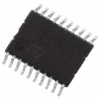


 工商网监
湘ICP备2023018690号
工商网监
湘ICP备2023018690号
