ACST8
®
ASD™
(AC Switch Family)
OVER VOLTAGE PROTECTED
AC POWER SWITCH
MAIN APPLICATIONS
■
■
■
AC static switching in appliance & industrial
control systems
Washing machine with bi-rotational induction
motor drive
Induction motor drive for:
- refrigerator / freezer compressor
- air conditioning compressor
OUT
G
TO-220FPAB
ACST8-8CFP
FEATURES
■
VDRM /VRRM = +/- 800V
■
Avalanche controlled device
IT(RMS) = 8A with TCASE = 90 °C
■
■
■
■
G
OUT
COM
OUT
COM
TO-220AB
ACST8-8CT
OUT
High noise immunity: static dV/dt > 750 V/µs
Gate triggering current : IGT < 30 mA
G
Snubberless turn off commutation:
(dI/dt)c > 4.5A/ms
COM
2
D PAK
ACST8-8CG
BENEFITS
■
■
■
■
Enables equipment to meet EN61000-4-5
standard
High off-state reliability with planar technology
Need no external overvoltage protection
Reduces the power component count
Table 1: Order Codes
Part Number
Marking
ACST8-8CFP
ACST8-8CT
DESCRIPTION
The ACST8-8C belongs to the AC power switch
family built around the ASDTM technology. This
high performance device is adapted to home appliances or industrial systems and drives an induction motor up to 8A.
This ACST switch embeds a triac structure with a
high voltage clamping device to absorb the inductive turn off energy and withstand line transients
such as those described in the IEC61000-4-5
standards.
ACST88C
ACST8-8CG
Figure 1: Functional Diagram
OUT
G
COM
TM: ASD is a trademark of STMicroelectronics.
November 2004
REV. 6
1/10
�ACST8
Table 2: Absolute Ratings (limiting values)
Symbol
IT(RMS)
Parameter
TO-220FPAB
RMS on-state current full cycle sine
TO-220AB /
wave 50 to 60 Hz
D2PAK
Tcase = 90°C
Value
8
Tcase = 100°C
8
tp = 20ms
tp = 16.7ms
tp = 10ms
80
85
35
A
A
A 2s
Rate period > 1mn
100
A/µs
note 1
2
- 40 to + 150
- 40 to + 125
260
kV
°C
°C
°C
Non repetitive surge peak on-state current
Tj initial = 25°C, full cycle sine wave
ITSM
I2t
Thermal constraint for fuse selection
Non repetitive on-state current critical rate of rise
IG = 10mA (tr < 100ns)
Non repetitive line peak pulse voltage
Storage temperature range
Operating junction temperature range
Maximum lead soldering temperature during 10s
dI/dt
VPP
Tstg
Tj
Tl
Unit
A
Note 1: according to test described by IEC61000-4-5 standard & figure A.
Table 3: Gate Characteristics (maximum values)
Symbol
Parameter
Average gate power dissipation
PG (AV)
PGM
Peak gate power dissipation (tp = 20µs)
Peak gate current (tp = 20µs)
IGM
Value
0.1
10
1
Unit
W
W
A
Table 4: Thermal Resistance
Symbol
Value
Unit
60
°C/W
45
3.5
°C/W
°C/W
2.5
°C/W
Rth(j-a)
Rth(j-a)
Rth(j-c)
Rth(j-c)
Parameter
TO-220FPAB
Junction to ambient
TO-220AB
2
Junction to ambien (soldered on 1 cm copper pad) D2PAK
Junction to case for full cycle sine wave conduction TO-220FPAB
TO-220AB
Junction to case for full cycle sine wave conduction 2
D PAK
Table 5: Parameter Description
Parameter Symbol
IGT
Gate triggering current
VGT
Gate triggering voltage
VGD
Non triggering voltage
IH
Holding current
IL
Latching current
VTM
On state voltage
VT0
On state characteristic threshold voltage
Rd
On state characteristic dynamic resistance
IDRM / IRRM
dV/dt
(dI/dt)c
VCL
2/10
Parameter description
Forward or reverse leakage current
Static pin OUT voltage rise
Turn off current rate of decay
Avalanche voltage at turn off
�ACST8
Table 6: Electrical Characteristics per Switch
For either positive or negative polary of pin OUT voltage respect to pin COM voltage
Symbol
VDRM/
VRRM
Test conditions
Repetitive peak off-state voltage
Values
Unit
MAX.
800
V
IGT
VOUT = 12V (DC) RL = 33Ω
Tj = 25°C
MAX.
30
mA
VGT
VOUT = 12V (DC) RL = 33Ω
Tj = 25°C
MAX.
1.5
V
VGD
VOUT = VDRM
RL = 3.3kΩ
Tj = 125°C
MIN.
0.2
V
IH
IOUT = 100mA
Gate open
Tj = 25°C
MAX.
40
mA
IL
IG = 20mA
Tj = 25°C
MAX.
70
mA
VTM
IOUT = 11A
Tj = 25°C
MAX.
1.5
V
VT0
Tj = 125°C
MAX.
0.95
V
Rd
Tj = 125°C
MAX.
50
mΩ
Tj = 25°C
MAX.
10
µA
Tj = 125°C
MAX.
1
mA
Tj = 125°C
MIN.
750
V/µs
Tj = 125°C
MIN.
4.5
A/ms
Tj = 25°C
TYP.
1200
V
IDRM /
IRRM
VOUT = VDRM
VOUT = VRRM
dV/dt
VOUT = 550V
(dI/dt)c
VCL
tp = 380µs
gate open
Without snubber
ICL = 1mA
tp = 1ms
1. AC LINE SWITCH BASIC APPLICATION
The ACST8-8C device is especially designed to drive medium power induction motors in washing machines, refrigerators, dish washers, and tumble dryers.
Pin COM
Pin G
Pin OUT
: Common drive reference, to be connected to the power line neutral
: Switch Gate input to be connected to the controller
: Switch Output to be connected to the load
When driven from a low voltage controller, the ACST switch is triggered with a negative gate current flowing out of the gate pin G. It can be driven by the controller through a resistor as shown on the typical application diagram. In appliance systems, the ACST8-8C switch intends to drive medium power load in ON /
OFF full cycle or phase angle control mode.
Thanks to its thermal and turn-off commutation characteristics, the ACST8-8C switch is able to drive an
inductive load up to 8A without a turn-off aid snubber circuit.
In washing machine or drier appliances, the tumble rotates in both directions. When using bidirectional
phase shift induction motor, two switches are connected on each side of the phase shift capacitor: in
steady-state operation, one switch only conducts energising the coils and defining the tumble direction.
3/10
�ACST8
Figure 2: Typical Application Diagram
OUT
G
COM
CONTROL
UNIT
2. ROBUSTNESS AGAINST FAST CAPACITOR DISCHARGE
When parasitic transients or controller mis-operation occur, the blocked switch may turn on by spurious
switch firing. Since the phase shift capacitor is charged, its energy is instantaneously dissipated through
the two ACSTs which can be destroyed. To prevent such a failure, a resistive inductive circuit R-L is added
in series with the phase shift capacitor.
The dI/dt depends on the maximal voltage Vmax of the phase shift capacitor (700V on 240V mains applications), and on the inductance L:
v max
dl
---- = -----------
L
dt
The total switch turn on di/dt is the sum of the di/dt created by any RC noise suppressor discharge and
the dI/dt created by the motor capacitor discharge.
Since the maximal dI/dt capability at turn-on of the ACST8 is 100A/µs, the motor capacitor di/dt is assumed
to be less than 50A/µs; therefore, the inductance should be 14µH.
The resistor R limits the surge current through the ACST8 during the capacitor discharge according to the
specified curve ITSM = f (tp) as shown in figure 11 (to be issued), and 1.2Ω is low enough to limit the resistor
dissipation (usually less than 1 W).
Finally both the 14µH inductance and the 1.2Ω resistance provide a safety margin of two on the surge current ITSM described in figure 11.
M
VAC
C
L
R
700V
T1
ON
4/10
T2
Fast capacitor discharge when
one ACST switch turns on (T2)
and the motor runs (T1 ON).
�ACST8
3. AC LINE TRANSIENT VOLTAGE RUGGEDNESS
The ACST8-8C switch is able to safely withstand the AC line transient voltages either by clamping the low
energy spikes or by breaking over under high energy shocks.
The test circuit in figure 3 is representative of the ACST application and is used to test the ACST switch
according to the IEC61000-4-5 standard conditions. Thanks to the load impedance, the ACST switch withstands voltage spikes up to 2 kV above the peak line voltage by breaking over safely. Such non repetitive
testing can be done 10 times on each AC line voltage polarity.
Figure 3: Overvoltage ruggedness test circuit for resistive and inductive loads according to
IEC61000-4-5 standard R = 47Ω, L = 10µH & VPP = 2kV
L
R
OUT
SURGE VOLTAGE
AC LINE & GENERATOR
VAC + V PP
G
COM
Figure 4: Maximum power dissipation versus
RMS on-state current
Figure 5: RMS on-state current versus case
temperature
P(W)
IT(RMS)(A)
11
9
α=180°
10
2
TO-220AB/D PAK
8
9
7
TO-220FPAB
8
6
7
6
5
5
4
4
3
3
180°
2
1
2
α
α
0
1
2
3
α=180°
1
IT(RMS)(A)
TC(°C)
0
0
4
5
6
7
8
Figure 6: RMS on-state current versus ambient
temperature
0
25
50
75
100
125
Figure 7: Relative variation of thermal
impedance versus pulse duration (TO-220FPAB)
K=[Zth/Rth]
IT(RMS)(A)
1.E+00
3.0
2.5
α=180°
Printed circuit board FR4
Natural convection
D2PAK
Zth(j-c)
1.E-01
2.0
Zth(j-a)
1.5
TO-220FPAB/TO-220AB
1.0
1.E-02
0.5
Tamb(°C)
0.0
0
25
50
75
TO-220FPAB
tp(°C)
100
125
1.E-03
1.E-03
1.E-02
1.E-01
1.E+00
1.E+01
1.E+02
1.E+03
5/10
�ACST8
Figure 8: Relative variation of thermal
impedance versus pulse duration (TO-220AB /
D2PAK)
Figure 9: On-state characteristics (maximum
values)
Iout(A)
K=[Zth/Rth]
1.E+00
100
Zth(j-c)
Tj=25°C
Tj=125°C
1.E-01
10
Zth(j-a)
Tj max. :
Vto = 0.95 V
Rd = 50 mΩ
2
TO-220AB/D PAK
tp(°C)
tp(°C)
1.E-02
1
1.E-03
1.E-02
1.E-01
1.E+00
1.E+01
1.E+02
1.E+03
Figure 10: Surge peak on-state current versus
number of cycles
0
1
2
3
4
5
6
Figure 11: Non repetitive surge peak on-state
current for a sinusoidal pulse with width tp <
10ms, and corresponding value of I2t
ITSM(A)
2
2
ITSM(A), I t (A s)
90
1000
Tj initial=25°C
80
70
t=20ms
Non repetitive
Tj initial=25°C
dI/dt limitation:
100A/µs
60
ITSM
50
100
40
Repetitive
Tc=90°C
30
I2t
20
10
Number of cycles
tp(ms)
0
10
1
10
100
1000
Figure 12: Relative variation of gate trigger
current, holding current and latching current
versus junction temperature (typical values)
0.01
1.00
10.00
Figure 13: Relative variation of critical rate of
decrease of main current versus reapplied dV/
dt (typical values)
IGT, IH,IL[Tj/IGT, IH, IL[Tj=25°C]
3.0
0.10
(dI/dt)c[(dV/dt)c] / Specified (dI/dt)c
5
2.5
4
IGT & IH
2.0
3
1.5
2
IL
1.0
1
0.5
Tj(°C)
0.0
dV/dt(V/µs)
0
-40 -30 -20 -10
6/10
0
10 20 30 40 50 60 70 80 90 100 110 120 130
0.1
1.0
10.0
100.0
�ACST8
Figure 14: Relative variation of critical rate of
decrease of main current versus junction
temperature
Figure 15: Relative variation of static dV/dt
versus junction temperature
(dI/dt)c[Tj] / (dI/dt)c[Tj=125°C]
3.5
6
dV/dt[Tj] / dV/dt[Tj=125°C]
Vout=550V
3.0
5
2.5
4
2.0
3
1.5
2
1.0
1
0.5
Tj(°C)
Tj(°C)
0.0
0
0
25
50
75
100
125
0
25
50
75
100
125
Figure 16: Surge peak on-state current versus
number of cycles
Rth(j-a)(°C/W)
80
70
60
50
40
30
20
10
S(Cu)(cm²)
0
0
5
10
15
20
25
30
35
40
Figure 17: Ordering Information Scheme
ACS T 8 - 8 C FP
AC Switch
Topology
T = Triac
RMS on-state current
8 = 8A
Repetitive peak off-state voltage
8 = 800V
Triggering gate current
C = 30mA
Package
FP = TO-220FPAB
CT = TO-220AB
CG = D2PAK
7/10
�ACST8
Figure 18: TO-220AB Package Mechanical Data
REF.
A
H2
Dia
C
L5
L7
L6
L2
F2
F1
D
L9
L4
F
M
G1
E
G
A
B
D
E
F
F1
F2
G
G1
H2
L2
L4
L5
L6
L7
L9
M
Diam.
DIMENSIONS
Millimeters
Inches
Min.
Max.
Min.
Max.
4.40
4.60
0.173
0.181
1.23
1.32
0.048
0.051
2.40
2.72
0.094
0.107
0.49
0.70
0.019
0.027
0.61
0.88
0.024
0.034
1.14
1.70
0.044
0.066
1.14
1.70
0.044
0.066
4.95
5.15
0.194
0.202
2.40
2.70
0.094
0.106
10
10.40
0.393
0.409
16.4 typ.
0.645 typ.
13
14
0.511
0.551
2.65
2.95
0.104
0.116
15.25
15.75
0.600
0.620
6.20
6.60
0.244
0.259
3.50
3.93
0.137
0.154
2.6 typ.
0.102 typ.
3.75
3.85
0.147
0.151
Figure 19: TO-220FPAB Package Mechanical Data
REF.
A
B
H
Dia
L6
L2
L7
L3
L5
D
F1
L4
F2
F
G1
G
8/10
E
A
B
D
E
F
F1
F2
G
G1
H
L2
L3
L4
L5
L6
L7
Dia.
DIMENSIONS
Millimeters
Inches
Min.
Max.
Min.
Max.
4.4
4.6
0.173
0.181
2.5
2.7
0.098
0.106
2.5
2.75
0.098
0.108
0.45
0.70
0.018
0.027
0.75
1
0.030
0.039
1.15
1.70
0.045
0.067
1.15
1.70
0.045
0.067
4.95
5.20
0.195
0.205
2.4
2.7
0.094
0.106
10
10.4
0.393
0.409
16 Typ.
0.63 Typ.
28.6
30.6
1.126
1.205
9.8
10.6
0.386
0.417
2.9
3.6
0.114
0.142
15.9
16.4
0.626
0.646
9.00
9.30
0.354
0.366
3.00
3.20
0.118
0.126
�ACST8
Figure 20: D2PAK Package Mechanical Data
REF.
A
E
C2
L2
D
L
L3
A1
B2
R
C
B
G
A2
M
*
V2
* FLAT ZONE NO LESSTHAN 2mm
A
A1
A2
B
B2
C
C2
D
E
G
L
L2
L3
M
R
DIMENSIONS
Millimeters
Inches
Min.
Max.
Min.
Max.
4.40
4.60
0.173
0.181
2.49
2.69
0.098
0.106
0.03
0.23
0.001
0.009
0.70
0.93
0.027
0.037
1.14
1.70
0.045
0.067
0.45
0.60
0.017
0.024
1.23
1.36
0.048
0.054
8.95
9.35
0.352
0.368
10.00
10.40
0.393
0.409
4.88
5.28
0.192
0.208
15.00
15.85
0.590
0.624
1.27
1.40
0.050
0.055
1.40
1.75
0.055
0.069
2.40
3.20
0.094
0.126
0.40 typ.
0.016 typ.
Figure 21: Foot Print Dimensions
(in millimeters)
16.90
10.30
5.08
1.30
3.70
8.90
Table 7: Ordering Information
Part Number
Marking
ACST8-8CFP
ACST8-8CT
ACST8-8CG
ACST88C
ACST8-8CG-TR
■
Package
Weight
Base qty
Delivery mode
TO-220FPAB
2.4 g
50
Tube
TO-220AB
2.3 g
50
Tube
D2PAK
1.5 g
50
Tube
500
Tape & reel
Epoxy meets UL94, V0
Table 8: Revision History
Date
Revision
Description of Changes
Jan-2002
4B
08-Nov-2004
5
TO-220AB and D2PAK packages added.
24-Nov-2004
6
Table 6 page 3 : IGT parameter added
Last update.
9/10
�ACST8
Information furnished is believed to be accurate and reliable. However, STMicroelectronics assumes no responsibility for the consequences
of use of such information nor for any infringement of patents or other rights of third parties which may result from its use. No license is granted
by implication or otherwise under any patent or patent rights of STMicroelectronics. Specifications mentioned in this publication are subject
to change without notice. This publication supersedes and replaces all information previously supplied. STMicroelectronics products are not
authorized for use as critical components in life support devices or systems without express written approval of STMicroelectronics.
The ST logo is a registered trademark of STMicroelectronics.
All other names are the property of their respective owners
© 2004 STMicroelectronics - All rights reserved
STMicroelectronics group of companies
Australia - Belgium - Brazil - Canada - China - Czech Republic - Finland - France - Germany - Hong Kong - India - Israel - Italy - Japan Malaysia - Malta - Morocco - Singapore - Spain - Sweden - Switzerland - United Kingdom - United States of America
www.st.com
10/10
�
很抱歉,暂时无法提供与“ACST8-8CG-TR”相匹配的价格&库存,您可以联系我们找货
免费人工找货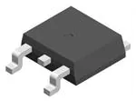


 工商网监
湘ICP备2023018690号
工商网监
湘ICP备2023018690号
