®
BUL310FP
HIGH VOLTAGE FAST-SWITCHING NPN POWER TRANSISTOR
s
s s s s
s s s s s
STMicroelectronics PREFERRED SALESTYPE NPN TRANSISTOR HIGH VOLTAGE CAPABILITY LOW SPREAD OF DYNAMIC PARAMETERS MINIMUM LOT-TO-LOT SPREAD FOR RELIABLE OPERATION VERY HIGH SWITCHING SPEED FULLY CHARACTERIZED AT 125oC LARGE RBSOA FULLY MOLDED INSULATED PACKAGE 2000 V DC INSULATION (U.L. COMPLIANT)
3 1 2
TO-220FP
APPLICATIONS HORIZONTAL DEFLECTION FOR COLOUR TV s ELECTRONIC BALLASTS FOR FLUORESCENT LIGHTING s FLYBACK AND FORWARD SINGLE TRANSISTOR LOW POWER CONVERTERS
s
INTERNAL SCHEMATIC DIAGRAM
DESCRIPTION The BUL310FP is manufactured using high voltage Multi Epitaxial Planar technology for high switching speeds and high voltage capability. It uses a Cellular Emitter structure with planar edge termination to enhance switching speeds while maintaining a wide RBSOA. The BUL series is designed for use in lighting applications and low cost switch-mode power supplies. ABSOLUTE MAXIMUM RATINGS
Symbol V CES V CEO V EBO IC I CM IB I BM P tot T stg Tj April 2003 Parameter Collector-Emitter Voltage (V BE = 0 ) Collector-Emitter Voltage (I B = 0 ) Emitter-Base Voltage (I C = 0 ) Collector Current Collector Peak Current (t p < 5 ms) Base Current Base Peak Current (t p < 5 ms) Total Dissipation at Tc = 25 o C Storage Temperature Max. Operating Junction Temperature Value 1000 500 9 5 10 3 4 36 -65 to 150 150 Unit V V V A A A A W o C o C 1/6
�BUL310FP
THERMAL DATA
R thj-case R thj-amb Thermal Resistance Junction-Case Thermal Resistance Junction-Ambient Max Max 3.5 62.5
o o
C/W C/W
ELECTRICAL CHARACTERISTICS (Tcase = 25 oC unless otherwise specified)
Symbol I CES I CEO Parameter Collector Cut-off Current (V BE = 0 ) Collector Cut-off Current (I B = 0 ) Test Conditions V CE = 1 000 V V CE = 1 000 V V CE = 5 00 V I C = 1 00 mA L= 25 mH 500 T j = 1 25 o C Min. Typ. Max. 100 500 250 Unit µA µA µA V
V CEO(sus) ∗ Collector-Emitter Sustaining Voltage (I B = 0 ) V EBO V CE(sat) ∗ Emitter-Base Voltage (I C = 0 ) Collector-Emitter Saturation Voltage Base-Emitter Saturation Voltage DC Current Gain INDUCTIVE LOAD Storage Time Fall Time INDUCTIVE LOAD Storage Time Fall Time
I E = 1 0 mA IC = 1 A IC = 2 A IC = 3 A IC = 1 A IC = 2 A IC = 3 A I C = 1 0 mA IC = 3 A IC = 2 A V BE(off) = -5 V V CL = 2 50 V (see figure 1) IC = 2 A V BE(off) = -5V V CL = 2 50 V T j = 1 25 o C I B = 0 .2 A I B = 0 .4 A I B = 0 .6 A I B = 0 .2 A I B = 0 .4 A I B = 0 .6 A VCE = 5 V V CE = 2 .5 V I B1 = 0 .4 A R BB = 0 Ω L = 200 µ H I B1 = 0 .4 A R BB = 0 Ω L = 200 µ H (see figure 1)
9 0.5 0.7 1.1 1 1.1 1.2 10 6 10 1.2 80 14 1.9 160
V V V V V V V
V BE(sat) ∗
h FE ∗
ts tf
µs ns
ts tf
1.8 150
µs ns
∗ Pulsed: Pulse duration = 300 µs, duty cycle 1.5 %
Safe Operating Areas
Derating Curve
2/6
�BUL310FP
DC Current Gain DC Current Gain
Collector Emitter Saturation Voltage
Base Emitter Saturation Voltage
Inductive Load Fall Time
Inductive Load Storage Time
3/6
�BUL310FP
Reverse Biased SOA
Figure 1: Inductive Load Switching Test Circuit
(1) Fast electronic switch (2) Non-inductive Resistor (3) Fast recovery rectifier
4/6
�BUL310FP
TO-220FP MECHANICAL DATA
DIM. MIN. A B D E F F1 F2 G G1 H L2 L3 L4 L6 L7 Ø 28.6 9.8 15.9 9 3 4.4 2.5 2.5 0.45 0.75 1.15 1.15 4.95 2.4 10 16 30.6 10.6 16.4 9.3 3.2 1.126 0.385 0.626 0.354 0.118 mm TYP. MAX. 4.6 2.7 2.75 0.7 1 1.7 1.7 5.2 2.7 10.4 MIN. 0.173 0.098 0.098 0.017 0.030 0.045 0.045 0.195 0.094 0.393 0.630 1.204 0.417 0.645 0.366 0.126 inch TYP. MAX. 0.181 0.106 0.108 0.027 0.039 0.067 0.067 0.204 0.106 0.409
A
B
L3 L6 L7
F1
D
¯
H
F
G1
E F2
123 L2 L4
G
5/6
�BUL310FP
Information furnished is believed to be accurate and reliable. However, STMicroelectronics assumes no responsibility for the consequences of use of such information nor for any infringement of patents or other rights of third parties which may result from its use. No license is granted by implication or otherwise under any patent or patent rights of STMicroelectronics. Specification mentioned in this publication are subject to change without notice. This publication supersedes and replaces all information previously supplied. STMicroelectronics products are not authorized for use as critical components in life support devices or systems without express written approval of STMicroelectronics. The ST logo is a trademark of STMicroelectronics © 2003 STMicroelectronics – Printed in Italy – All Rights Reserved STMicroelectronics GROUP OF COMPANIES Australia - Brazil - Canada - China - Finland - France - Germany - Hong Kong - India - Israel - Italy - Japan - Malaysia - Malta - Morocco Singapore - Spain - Sweden - Switzerland - United Kingdom - United States. http://www.st.com
6/6
�
很抱歉,暂时无法提供与“BUL310FP”相匹配的价格&库存,您可以联系我们找货
免费人工找货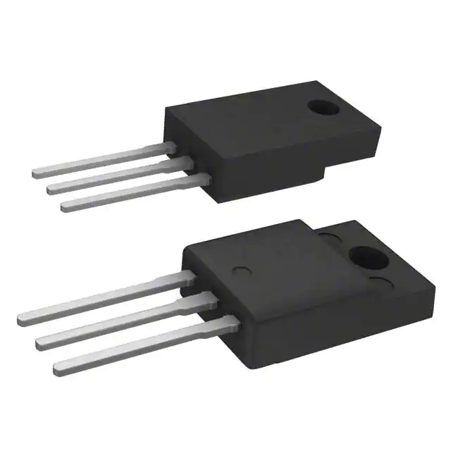


 工商网监
湘ICP备2023018690号
工商网监
湘ICP备2023018690号
