DSM2150F5V
DSM (Digital Signal Processor System Memory)
for Analog Devices DSPs (3.3V Supply)
FEATURES SUMMARY
■
■
■
■
■
■
Glueless Connection to DSP
– Easily add memory, logic, and I/O to the
External Port of ADSP-218x, 219x, 2106x,
2116x, 2153x, and TS101 families of
DSPs from Analog Devices, Inc.
Dual Flash Memories
– Two independent Flash memory arrays
for storing DSP code and data
– Capable of read-while-write concurrent
Flash memory operation
– Device can be configured as 8-bit or 16-bit
– Built-in programmable address decoding
logic allows mapping individual sectors of
each Flash array to any address boundary
– Each Flash sector can be write protected
512 KByte Main Flash memory
– Ample storage for boot loading DSP code/
data upon reset and subsequent code
swaps
– Large capacity for storing tables and
constants or for data recording
32 KByte Secondary Flash memory
– Smaller sector size ideal for storing
calibration and configuration constants.
Eliminate external serial EEPROM.
– Optionally bypass internal DSP boot ROM
during start-up and execute code directly
from Secondary Flash. Use for custom
start-up code and In-Application
Programming (IAP).
Up to 40 Multifunction I/O Pins
– Increase total DSP system I/O capability
– I/O controlled by DSP software or PLD
logic
General purpose PLD
– Use for peripheral glue logic to keypads,
control panel, displays, LCDs, and other
devices
– Over 3,000 gates of PLD with 16 macro
cells
– Eliminate PLDs and external logic devices
– Create state machines, chip selects,
simple shifters and counters, clock
dividers, delays
– Simple PSDsoft Express™ development
software, free from www.st.com/psm
August 2004
Figure 1. TQFP 80-pin Package
TQFP80 (T)
■
■
■
■
■
In-System Programming (ISP) with JTAG
– Program entire chip in 15-35 seconds with
no involvement of the DSP
– Optionally links with DSP JTAG debug
port
– Eliminate need for sockets and preprogramming of memory and logic
devices
– ISP allows efficient manufacturing and
product testing supporting Just-In-Time
inventory
– Use low-cost FlashLINK™ cable with any
PC. Available from www.st.com/psm.
Content Security
– Programmable Security Bit blocks access
of device programmers and readers
Operating Range
– VCC: 3.3V ± 10%, Temp: –40°C to +85°C
Zero-Power Technology
– 50µA standby current typical
Flash Memory Speed, Endurance, Retention
– 120ns, 100K cycles, 15 year retention
1/73
�DSM2150F5V
TABLE OF CONTENTS
FEATURES SUMMARY . . . . . . . . . . . . . . . . . . . . . . . . . . . . . . . . . . . . . . . . . . . . . . . . . . . . . . . . . . . . . 1
SUMMARY DESCRIPTION . . . . . . . . . . . . . . . . . . . . . . . . . . . . . . . . . . . . . . . . . . . . . . . . . . . . . . . . . . . 5
PIN DESCRIPTION . . . . . . . . . . . . . . . . . . . . . . . . . . . . . . . . . . . . . . . . . . . . . . . . . . . . . . . . . . . . . . . . . 8
ARCHITECTURAL OVERVIEW . . . . . . . . . . . . . . . . . . . . . . . . . . . . . . . . . . . . . . . . . . . . . . . . . . . . . . 10
DSP Address/Data/Control Interface . . . . . . . . . . . . . . . . . . . . . . . . . . . . . . . . . . . . . . . . . . . . . . 10
Main Flash Memory . . . . . . . . . . . . . . . . . . . . . . . . . . . . . . . . . . . . . . . . . . . . . . . . . . . . . . . . . . . . 11
Secondary Flash Memory . . . . . . . . . . . . . . . . . . . . . . . . . . . . . . . . . . . . . . . . . . . . . . . . . . . . . . . 11
Programmable Logic (PLDs) . . . . . . . . . . . . . . . . . . . . . . . . . . . . . . . . . . . . . . . . . . . . . . . . . . . . 11
Runtime Control Registers . . . . . . . . . . . . . . . . . . . . . . . . . . . . . . . . . . . . . . . . . . . . . . . . . . . . . . 12
Memory Page Register . . . . . . . . . . . . . . . . . . . . . . . . . . . . . . . . . . . . . . . . . . . . . . . . . . . . . . . . . 12
I/O Ports . . . . . . . . . . . . . . . . . . . . . . . . . . . . . . . . . . . . . . . . . . . . . . . . . . . . . . . . . . . . . . . . . . . . . 12
JTAG ISP Port . . . . . . . . . . . . . . . . . . . . . . . . . . . . . . . . . . . . . . . . . . . . . . . . . . . . . . . . . . . . . . . . 12
Power Management. . . . . . . . . . . . . . . . . . . . . . . . . . . . . . . . . . . . . . . . . . . . . . . . . . . . . . . . . . . . 12
Security and NVM Sector Protection . . . . . . . . . . . . . . . . . . . . . . . . . . . . . . . . . . . . . . . . . . . . . . 12
RUNTIME CONTROL REGISTER DEFINITION . . . . . . . . . . . . . . . . . . . . . . . . . . . . . . . . . . . . . . . . . . 13
DETAILED OPERATION. . . . . . . . . . . . . . . . . . . . . . . . . . . . . . . . . . . . . . . . . . . . . . . . . . . . . . . . . . . . 14
Flash Memories . . . . . . . . . . . . . . . . . . . . . . . . . . . . . . . . . . . . . . . . . . . . . . . . . . . . . . . . . . . . . . . 14
INSTRUCTIONS . . . . . . . . . . . . . . . . . . . . . . . . . . . . . . . . . . . . . . . . . . . . . . . . . . . . . . . . . . . . . . . . . . 19
Reading Flash Memory . . . . . . . . . . . . . . . . . . . . . . . . . . . . . . . . . . . . . . . . . . . . . . . . . . . . . . . . . 20
Read Memory Contents . . . . . . . . . . . . . . . . . . . . . . . . . . . . . . . . . . . . . . . . . . . . . . . . . . . . . . . . 20
Read Main Flash Identifier . . . . . . . . . . . . . . . . . . . . . . . . . . . . . . . . . . . . . . . . . . . . . . . . . . . . . . 20
Read Memory Sector Protection Status . . . . . . . . . . . . . . . . . . . . . . . . . . . . . . . . . . . . . . . . . . . 20
Reading the Erase/Program Status Bits . . . . . . . . . . . . . . . . . . . . . . . . . . . . . . . . . . . . . . . . . . . 20
Data Polling Flag (DQ7). . . . . . . . . . . . . . . . . . . . . . . . . . . . . . . . . . . . . . . . . . . . . . . . . . . . . . . . . 20
Toggle Flag (DQ6) . . . . . . . . . . . . . . . . . . . . . . . . . . . . . . . . . . . . . . . . . . . . . . . . . . . . . . . . . . . . . 21
Error Flag (DQ5). . . . . . . . . . . . . . . . . . . . . . . . . . . . . . . . . . . . . . . . . . . . . . . . . . . . . . . . . . . . . . . 21
Erase Time-out Flag (DQ3) . . . . . . . . . . . . . . . . . . . . . . . . . . . . . . . . . . . . . . . . . . . . . . . . . . . . . . 21
PROGRAMMING FLASH MEMORY. . . . . . . . . . . . . . . . . . . . . . . . . . . . . . . . . . . . . . . . . . . . . . . . . . . 22
PLDs . . . . . . . . . . . . . . . . . . . . . . . . . . . . . . . . . . . . . . . . . . . . . . . . . . . . . . . . . . . . . . . . . . . . . . . . . . . 24
Turbo Bit. . . . . . . . . . . . . . . . . . . . . . . . . . . . . . . . . . . . . . . . . . . . . . . . . . . . . . . . . . . . . . . . . . . . . 24
Decode PLD (DPLD) . . . . . . . . . . . . . . . . . . . . . . . . . . . . . . . . . . . . . . . . . . . . . . . . . . . . . . . . . . . 26
Complex PLD (CPLD) . . . . . . . . . . . . . . . . . . . . . . . . . . . . . . . . . . . . . . . . . . . . . . . . . . . . . . . . . . 27
Output Macrocell (OMC) . . . . . . . . . . . . . . . . . . . . . . . . . . . . . . . . . . . . . . . . . . . . . . . . . . . . . . . . 28
Product Term Allocator. . . . . . . . . . . . . . . . . . . . . . . . . . . . . . . . . . . . . . . . . . . . . . . . . . . . . . . . . 29
Loading and Reading the OMCs . . . . . . . . . . . . . . . . . . . . . . . . . . . . . . . . . . . . . . . . . . . . . . . . . 29
The OMC Mask Register . . . . . . . . . . . . . . . . . . . . . . . . . . . . . . . . . . . . . . . . . . . . . . . . . . . . . . . . 31
2/73
�DSM2150F5V
The Output Enable of the OMC . . . . . . . . . . . . . . . . . . . . . . . . . . . . . . . . . . . . . . . . . . . . . . . . . . 31
Input Macrocells (IMC) . . . . . . . . . . . . . . . . . . . . . . . . . . . . . . . . . . . . . . . . . . . . . . . . . . . . . . . . . 31
DSP BUS INTERFACE . . . . . . . . . . . . . . . . . . . . . . . . . . . . . . . . . . . . . . . . . . . . . . . . . . . . . . . . . . . . . 33
Typical Memory Map, DSM2150F5V and ADSP21535 BLACKFIN DSP. . . . . . . . . . . . . . . . . . . 33
Specifying the Memory Map with PSDsoft Express™ . . . . . . . . . . . . . . . . . . . . . . . . . . . . . . . . 33
ADSP-21535 Blackfin DSP . . . . . . . . . . . . . . . . . . . . . . . . . . . . . . . . . . . . . . . . . . . . . . . . . . . . . . 36
ADSP-21062 SHARC DSP . . . . . . . . . . . . . . . . . . . . . . . . . . . . . . . . . . . . . . . . . . . . . . . . . . . . . . . 37
ADSP-TS101S TigerSHARC DSP . . . . . . . . . . . . . . . . . . . . . . . . . . . . . . . . . . . . . . . . . . . . . . . . . 38
ADSP-2191 . . . . . . . . . . . . . . . . . . . . . . . . . . . . . . . . . . . . . . . . . . . . . . . . . . . . . . . . . . . . . . . . . . . 39
ADSP-2188M . . . . . . . . . . . . . . . . . . . . . . . . . . . . . . . . . . . . . . . . . . . . . . . . . . . . . . . . . . . . . . . . . 40
I/O PORTS . . . . . . . . . . . . . . . . . . . . . . . . . . . . . . . . . . . . . . . . . . . . . . . . . . . . . . . . . . . . . . . . . . . . . . . 41
General Port Architecture . . . . . . . . . . . . . . . . . . . . . . . . . . . . . . . . . . . . . . . . . . . . . . . . . . .
Port Operating Modes . . . . . . . . . . . . . . . . . . . . . . . . . . . . . . . . . . . . . . . . . . . . . . . . . . . . . .
MCU I/O Mode . . . . . . . . . . . . . . . . . . . . . . . . . . . . . . . . . . . . . . . . . . . . . . . . . . . . . . . . . . . .
Drive Select Register. . . . . . . . . . . . . . . . . . . . . . . . . . . . . . . . . . . . . . . . . . . . . . . . . . . . . . .
DSP Data Bus. . . . . . . . . . . . . . . . . . . . . . . . . . . . . . . . . . . . . . . . . . . . . . . . . . . . . . . . . . . . .
PLD Inputs . . . . . . . . . . . . . . . . . . . . . . . . . . . . . . . . . . . . . . . . . . . . . . . . . . . . . . . . . . . . . . .
PLD Outputs. . . . . . . . . . . . . . . . . . . . . . . . . . . . . . . . . . . . . . . . . . . . . . . . . . . . . . . . . . . . . .
JTAG In-System Programming (ISP) . . . . . . . . . . . . . . . . . . . . . . . . . . . . . . . . . . . . . . . . . .
Enable Out . . . . . . . . . . . . . . . . . . . . . . . . . . . . . . . . . . . . . . . . . . . . . . . . . . . . . . . . . . . . . . .
Ports A, B, and C – Functionality and Structure . . . . . . . . . . . . . . . . . . . . . . . . . . . . . . . .
Port D – Functionality and Structure . . . . . . . . . . . . . . . . . . . . . . . . . . . . . . . . . . . . . . . . . .
Port E – Functionality and Structure . . . . . . . . . . . . . . . . . . . . . . . . . . . . . . . . . . . . . . . . . .
Port F – Functionality and Structure . . . . . . . . . . . . . . . . . . . . . . . . . . . . . . . . . . . . . . . . . .
Port G – Functionality and Structure . . . . . . . . . . . . . . . . . . . . . . . . . . . . . . . . . . . . . . . . . .
. . . . 41
. . . . 41
. . . . 42
. . . . 43
. . . . 43
. . . . 43
. . . . 43
. . . . 43
. . . . 43
. . . . 44
. . . . 45
. . . . 46
. . . . 46
. . . . 46
POWER MANAGEMENT . . . . . . . . . . . . . . . . . . . . . . . . . . . . . . . . . . . . . . . . . . . . . . . . . . . . . . . . . . . 47
RESET TIMING AND DEVICE STATUS AT RESET . . . . . . . . . . . . . . . . . . . . . . . . . . . . . . . . . . . . . . 48
Power On Reset . . . . . . . . . . . . . . . . . . . . . . . . . . . . . . . . . . . . . . . . . . . . . . . . . . . . . . . . . . . . . . . 48
Warm Reset . . . . . . . . . . . . . . . . . . . . . . . . . . . . . . . . . . . . . . . . . . . . . . . . . . . . . . . . . . . . . . . . . . 48
I/O Pin, Register, and PLD Status at Reset . . . . . . . . . . . . . . . . . . . . . . . . . . . . . . . . . . . . . . . . . 48
PROGRAMMING IN-CIRCUIT USING JTAG ISP. . . . . . . . . . . . . . . . . . . . . . . . . . . . . . . . . . . . . . . . . 49
Standard JTAG Signals. . . . . . . . . . . . . . . . . . . . . . . . . . . . . . . . . . . . . . . . . . . . . . . . . . . . . . . . . 49
JTAG Extensions . . . . . . . . . . . . . . . . . . . . . . . . . . . . . . . . . . . . . . . . . . . . . . . . . . . . . . . . . . . . . . 50
INITIAL DELIVERY STATE. . . . . . . . . . . . . . . . . . . . . . . . . . . . . . . . . . . . . . . . . . . . . . . . . . . . . . . . . . 50
AC AND DC PARAMETERS. . . . . . . . . . . . . . . . . . . . . . . . . . . . . . . . . . . . . . . . . . . . . . . . . . . . . . . . . 51
MAXIMUM RATING. . . . . . . . . . . . . . . . . . . . . . . . . . . . . . . . . . . . . . . . . . . . . . . . . . . . . . . . . . . . . . . . 52
DC AND AC OPERATING AND MEASUREMENT CONDITIONS . . . . . . . . . . . . . . . . . . . . . . . . . . . . 53
3/73
�DSM2150F5V
PACKAGE MECHANICAL . . . . . . . . . . . . . . . . . . . . . . . . . . . . . . . . . . . . . . . . . . . . . . . . . . . . . . . . . . 65
PART NUMBERING . . . . . . . . . . . . . . . . . . . . . . . . . . . . . . . . . . . . . . . . . . . . . . . . . . . . . . . . . . . . . . . 67
APPENDIX A.TQFP80 PIN ASSIGNMENTS . . . . . . . . . . . . . . . . . . . . . . . . . . . . . . . . . . . . . . . . . . . . 68
APPENDIX B.CSIOP REGISTER BIT DEFINITIONS . . . . . . . . . . . . . . . . . . . . . . . . . . . . . . . . . . . . . . 69
REVISION HISTORY. . . . . . . . . . . . . . . . . . . . . . . . . . . . . . . . . . . . . . . . . . . . . . . . . . . . . . . . . . . . . . . 72
4/73
�DSM2150F5V
SUMMARY DESCRIPTION
The DSM2150F5V is an 8 or 16-bit system memory device for use with the Analog Devices DSPs.
DSM means Digital signal processor System
Memory. A DSM device brings In-System Programmable (ISP) Flash memory, parameter storage, programmable logic, and additional I/O to
DSP systems. The result is a flexible two-chip solution for DSP designs. On-chip integrated memory decode logic makes it easy to map dual banks
of Flash memory to the DSPs in a variety of ways
for bootloading or bypassing DSP boot ROM, code
execution, data recording, code swapping, and
parameter storage.
JTAG ISP reduces development time, simplifies
manufacturing flow, and lowers the cost of field upgrades. The JTAG ISP interface eliminates the
need for sockets and pre-programmed memory
and logic devices. End products may be manufactured with a blank DSM device soldered down and
programmed at the end of the assembly line in 15
to 35 seconds with no involvement of the DSP.
Rapidly program test code, then application code
as determined by Just-In Time inventory requirements. Additionally, JTAG ISP reduces development time by turning fast iterations of DSP code in
the lab. Code updates in the field require no product disassembly. The FlashLINK™ JTAG programming cable costs $59 USD and plugs into any PC
parallel port. Programming through conventional
device insertion programmers is also available using PSDpro from STMicroelectronics and other 3rd
party programmers. See www.st.com/psm.
DSM devices add programmable logic (PLD) and
up to 32 configurable I/O pins to the DSP system.
The state of I/O pins can be driven by DSP software or PLD logic. PLD and I/O configuration are
programmable by JTAG ISP. The PLD consists of
more than 3000 gates and has 16 macro cell registers. Common uses for the PLD include chip-selects for external devices, state-machines, simple
shiftier and counters, keypad and control panel interfaces, clock dividers, handshake delay, muxes,
etc., eliminating the need for small external PLDs
and logic devices. Configuration of PLD, I/O, and
Flash memory mapping is easily entered in a
point-and-click environment using the software
development tool, PSDsoft Express™, available at
no charge from www.st.com/psm. The two-chip
DSP/DSM combination is ideal for systems having
limitations on size, EMI levels, and power consumption. DSM memory and logic are “zero-power”, meaning they automatically go to standby
between memory accesses or logic input changes, producing low active and standby current consumption, which is ideal for battery powered
products.
A programmable security bit in the DSM protects
its contents from unauthorized viewing and copying. When set, the security bit will block access of
programming devices (JTAG or others) to the
DSM Flash memories and PLD configuration. The
only way to defeat the security bit is to erase the
entire DSM device, after which the device is blank
and may be used again. The DSP will always have
access to Flash memory contents through the data
bus, even with security bit set.
Figure 2. System Block Diagram, Two Chip Solution
SERIAL
DEVICE
SERIAL
DEVICE
SDRAM
HOST
MCU
ANALOG
DEVICES
DSP
ADDRESS
CONTROL
ADSP-218x
ADSP-219x
ADSP-2153x
ADSP-2106x
ADSP-2116x
ADSP-TS101S
8 or 16 DATA
PRIMARY
FLASH MEMORY
512 Kbytes
SECONDARY
FLASH MEMORY
32 Kbytes
16 MACROCELL PLD
16 I/O
PORTS
WITH I/O, PLD, CHIP SELECTS
PLD
I/O BUS
I/O FLAGS
ADDR & DECODE
LOGIC
DSM2150F5V
DSP SYSTEM MEMORY
8 to 16
I/O
GENERAL PURPOSE I/O
PORTS
I/O CONTROL
POWER MANAGEMENT
CONTENT SECURITY
JTAG
ISP TO
ALL
AREAS
JTAG ISP
JTAG DEBUG (All But ADSP-218x Family)
AI05732
5/73
�DSM2150F5V
Table 1. DSM2150F5V DSP Memory System Devices
Part Number
Main Flash
Memory
Secondary
Flash Mem
PLD
I/O
Ports
VCC and I/O
Mem
Package Op Temp
Speed
DSM2150F5V-12T6
512 KBytes,
eight 64-KByte
sectors
32 KBytes,
four 8-KByte
sectors
16
macro
cells
Up to
40
3.3V ±10%
120ns
80-pin
TQFP
–40oC to
+85oC
Table 2. Compatible Analog Devices DSPs
DSP Part Number
Core Operating Voltage
I/O Voltage
ADSP-2183, 2184L, 2185L, 2186L, 2187L
3.3V
3.3V
ADSP-2185M, 2186M, 2188M, 2189M
2.5V
3.3V
ADSP-2184N, 2185N, 2186N, 2187N, 2188N, 2189N
1.8V
3.3V
ADSP-2191M, 2195M, 2196M
2.5V
3.3V
Blackfin ADSP-21532S
3.3V
3.3V
Blackfin ADSP-21535P
1.5V
3.3V
Sharc ADSP-21060L, 21061L, 21062L, 21065L
3.3V
3.3V
Sharc ADSP-21160M
2.5V
3.3V
Sharc ADSP-21160N, 21161N
1.8V
3.3V
Tiger Sharc ADSP-TS101S
1.0V
3.3V
6/73
�DSM2150F5V
61 PB0
62 PB1
63 PB2
64 PB3
65 PB4
66 PB5
67 PB6
69 VCC
68 PB7
70 GND
71 PE0
72 PE1
73 PE2
74 PE3
75 PE4
76 PE5
77 PE6
78 PE7
79 PD0
80 PD1
Figure 3. TQFP Connections
PD2 1
60 CNTL1
PD3 2
59 CNTL0
AD0 3
58 PA7
AD1 4
57 PA6
AD2 5
56 PA5
AD3 6
55 PA4
AD4 7
54 PA3
GND 8
53 PA2
VCC 9
AD5 10
52 PA1
AD6 11
50 GND
AD7 12
49 GND
AD8 13
48 PC7
AD9 14
47 PC6
AD10 15
46 PC5
AD11 16
45 PC4
AD12 17
44 PC3
AD13 18
43 PC2
AD14 19
42 PC1
AD15 20
41 PC0
CNTL2 40
RESET 39
PF7 38
PF6 37
PF5 36
PF4 35
PF3 34
PF2 33
PF1 32
PF0 31
VCC 29
GND 30
PG7 28
PG6 27
PG5 26
PG4 25
PG3 24
PG2 23
PG1 22
PG0 21
51 PA0
AI04943
7/73
�DSM2150F5V
PIN DESCRIPTION
Table 3. Pin Description (Pin Assignments in Appendix A)
Pin Name Type
AD0-15
In
CNTL0
In
Description
Sixteen address inputs from the DSP.
Active low WRITE strobe input from the DSP, typically connected to DSP WR signal.
Also functions as WRL for DSPs which use WRL strobe when writing low byte only in 16-bit word.
CNTL1
In
Active low READ strobe input from the DSP.
Programmable control input.
CNTL2
In
CNTL2 may be used for BHE (Byte High Enable) when DSM2150F5V is configured for 16-bit
operation. BHE = ’0’ will allow a byte WRITE from data lines D8-D15 ignoring data lines D0-D7.
BHE = 1 will allow a byte WRITE from D0-D7 ignoring data lines D8-D15. DSP READ operations
are not affected by BHE (always read both bytes).
Active low reset input from system.
Reset
PA0-7
PB0-7
PC0-7
PD0-3
8/73
In
Resets DSM I/O Ports, Page Register contents, and other DSM configuration registers. Must be
logic Low at Power-up.
I/O
Eight configurable Port A signals with the following functions:
– MCU I/O – DSP may write or read pins directly at runtime with csiop registers.
– CPLD Output Macrocell (McellA0-7) outputs.
– Inputs to the PLDs (via Input Macrocells). Can be used to input address A16 and above.
Note: PA0-PA7 may be configured at run-time as standard CMOS or Open Drain Outputs.
I/O
Eight configurable Port B signals with the following functions:
– MCU I/O – DSP may write or read pins directly at runtime with csiop registers.
– CPLD Output Macrocell (McellB0-7 or McellC0-7) outputs.
– Inputs to the PLDs (via Input Macrocells). Can be used to input address A16 and above.
Note: PB0-PB7 may be configured at run-time as standard CMOS or Open Drain Outputs.
I/O
Eight configurable Port C signals with the following functions:
– MCU I/O – DSP may write or read pins directly at runtime with csiop registers.
– DPLD chip-select outputs (ECS0-7, does not consume MicroCells).
– Inputs to the PLDs (via Input Macrocells). Can be used to input address A16 and above.
Note: PC0-PC7 may be configured at run-time as standard CMOS or Faster Slew Rate Output.
I/O
Four configurable Port D signals with the following functions:
– MCU I/O – DSP may write or read pins directly at runtime with csiop registers.
– Input to the PLDs (no associated Input Macrocells, routes directly into PLDs). Can be used to
input address A16 and above.
– PD1 can be configured as CLKIN, a common clock input to PLD.
– PD2 can be configured as CSI, active low Chip Select Input to select Flash memory. Flash
memory is disabled to conserve more power when CSI is logic high.
– PD3 can be used for WRH strobe from DSP to write high byte only for 16-bit configuration.
�DSM2150F5V
Pin Name Type
PE0-7
PF0-7
I/O
I/O
Description
Eight configurable Port E signals with the following functions:
– MCU I/O – DSP may write or read pins directly at runtime with csiop registers.
– PE0, PE1, PE2, and PE3 can form the JTAG IEEE-1149.1 ISP serial interface as signals TMS,
TCK, TDI, and TDO respectively.
– PE4 and PE5 can form the enhanced JTAG signals TSTAT and TERR respectively. Reduces
ISP programming time up to 30% when used in addition to the standard four JTAG signals: TDI,
TDO, TMS, TCK.
– PE4 can be configured as the Ready/Busy output to indicate Flash memory programming
status during parallel programming. May be polled by DSP or used as DSP interrupt.
Note 1: PE0-PE7 may be configured at run-time as either standard CMOS or Open Drain Outputs.
Note 2: The JTAG ISP pins may be multiplexed with other I/O functions.
Port F connects to eight data bus signals, D0 - D7 from DSP.
Port G connects to eight data bus signals, D8 - D15 from DSP if 16-bit data path is used.
PG0-7
I/O
Otherwise, PG0-PG7 can be used for general purpose MCU I/O pins.
Note: PG0-PG7 may be configured at run-time as standard CMOS or Open Drain Outputs.
VCC
Supply Voltage
GND
Ground pins
9/73
�DSM2150F5V
ARCHITECTURAL OVERVIEW
Major functional blocks are shown in Figure 4.
DSP Address/Data/Control Interface
These DSP signals attach directly to the DSM for
a glueless connection. An 8-bit or 16-bit data connection is formed and 16 or more DSP address
lines can be decoded as well as various DSP
memory strobes; i.e. BMS, RD, AWE, IOMS, MSx,
etc. The data path width must be specified as 8bits or 16-bits in PSDsoft Express. This configura-
tion is a static, meaning the data path width cannot
switch between 8-bits and 16-bits during runtime.
Port F is used for 8-bit data path, Ports F and G are
used for 16-bit data path. There are many different
ways the DSM2150F5V can be configured and
used depending on system requirements. See Appendices for example connections between the
DSM2150F5V and different DSPs.
Figure 4. Block Diagram
INTERNAL ADDR, DATA, CONTROL BUS LINKED TO DSP
DSP ADDR
AD0
AD1
AD2
AD3
AD4
AD5
AD6
AD7
AD8
AD9
AD10
AD11
AD12
AD13
AD14
AD15
I/O PORT
SECURITY
LOCK
TO PLD
IN BUS
PAGE REG
MAIN FLASH
DECODE
PLD
8 BLOCKS, 64 KB
512 KBytes total
FS0-7
4 BLOCKS, 8 KB
32 KBytes total
RUNTIME CONTROL
GPIO
PLD
POWER MNGMT
PLD INPUT BUS
I/O PORT
ECS0-7
PB0
PB1
PB2
PB3
PB4
PB5
PB6
PB7
GENERAL PLD
AND
ARRAY
DSP DATA
or GP I/O
PG0
PG1
PG2
PG3
PG4
PG5
PG6
PG7
PA0
PA1
PA2
PA3
PA4
PA5
PA6
PA7
CSBOOT0-3
CSIOP
PF0
PF1
PF2
PF3
PF4
PF5
PF6
PF7
I/O PORT
SECONDARY FLASH
DSP DATA
A
A A
A
A
A A A
B
B B
B
B
B B B
16 OUTPUT MICROCELLS
A
A
A
A
A
A
A
A
C
C
C
C
B
B
B
B
B
B
B
B
C
C
C
C
I/O PORT
PC0
PC1
PC2
PC3
PC4
PC5
PC6
PC7
24 INPUT
MICROCELLS
PIN FEEDBACK
DSP CNTL
CNTL0
CNTL1
CNTL2
RST\
PD0
PD1
PD2
PD3
NODE FEEDBACK
I/O PORT
INTERNAL ADDR, DATA, CONTROL BUS LINKED TO DSP
DSM2150F5V
DSP System Memory
JTAG ISP
CONTROLLER
PE0
PE1
PE2
PE3
PE4
PE5
PE6
PE7
AI05776
10/73
�DSM2150F5V
Main Flash Memory
The 4M bit (512 KByte) Main Flash memory is divided into eight equally-sized 64 KByte sectors
that are individually selectable through the Decode PLD. Each Flash memory sector can be located at any address as defined by the user with
PSDsoft Express. DSP code and data are easily
placed in flash memory using PSDsoft Express,
the software development tool.
Secondary Flash Memory
The 256Kbit (32 KByte) Secondary Flash memory
is divided into eight equally-sized 8 KByte sectors
that are individually selectable through the Decode PLD. Each Flash memory sector can be located at any address as defined by the user with
PSDsoft Express. DSP code and data can also be
placed Secondary Flash memory using the PSDsoft Express development tool.
Secondary flash memory is good for storing data
because of its smaller sectors. Software EEPROM
emulation techniques can be used for small data
sets that change frequently on a byte-by-byte basis.
Secondary flash may also be used to store custom
start-up code for applications that do not “boot” using DMA, but instead start executing code from external memory upon reset (bypass internal DSP
boot ROM). Storing code here can keep the entire
Main Flash free of initialization code for clean software partitioning. If only one or more 8 KByte sectors are needed for start-up code, the remaining
sectors of Secondary Flash may be used for data
storage.
In-Application-Programming (IAP) may be implemented using Secondary Flash. For example,
code to implement IAP over a USB channel may
be stored here. The DSP executes code from Secondary Flash array while erasing and writing new
code to the Main Flash array as it is received over
the USB channel. Any communication channel
that the DSP supports can be used for IAP.
Secondary Flash may also be used as an extension to Main Flash memory producing a total of
544 KBytes.
Miscellaneous: Main and Secondary Flash memories are totally independent, allowing concurrent
operation. The DSP can read from one memory
while erasing or programming the other. The DSP
can erase Flash memories by individual sectors or
the entire Flash memory array may be erased at
one time. Each sector in either Flash memory array may be individually write protected, blocking
any WRITEs from the DSP (good for boot and
start-up code protection). The Flash memories automatically go to standby between DSP READ or
WRITE accesses to conserve power. Maximum
access times include sector decoding time. Maxi-
mum erase cycles is 100K and data retention is 15
years minimum. Flash memory, as well as the entire DSM device may be programmed with the
JTAG ISP interface with no DSP involvement.
Programmable Logic (PLDs)
The DSM family contains two PLDS that may optionally run in Turbo or Non-Turbo Mode. PLDs operate faster (less propagation delay) while in
Turbo Mode but consume more power than NonTurbo Mode. Non-Turbo Mode allows the PLDs to
automatically go to standby when no inputs are
change to conserve power. The Turbo Mode setting is controlled at runtime by DSP software.
Decode PLD (DPLD). This is programmable logic used to select one of the eight individual Main
Flash memory segments, one of four individual
Secondary Flash memory segments, or the group
of control registers within the DSM device. The
DPLD can also drive external chip select signals
on Port C pins. DPLD input signals include: DSP
address and control signals, Page Register outputs, DSM Port Pins, CPLD logic feedback.
Complex PLD (CPLD). This programmable logic
is used to create both combinatorial and sequential general purpose logic. The CPLD contains 16
Output Macrocells (OMCs) and 24 Input Macrocells (IMCs). PSD Macrocell registers are unique
in that they have direct connection to the DSP data
bus allowing them to be loaded and read directly
by the DSP at runtime. This direct access is good
for making small peripheral devices (shiftier,
counters, state machines, etc.) that are accessed
directly by the DSP with little overhead. DPLD inputs include DSP address and control signals,
Page Register outputs, DSM Port Pins, and CPLD
feedback.
OMCs: The general structure of the CPLD is similar in nature to a 22V10 PLD device with the familiar sum-of-products (AND-OR) construct. True
and compliment versions of 73 input signals are
available to a large AND array. AND array outputs
feed into a multiple product-term OR gate within
each OMC (up to 10 product-terms for each
OMC). Logic output of the OR gate can be passed
on as combinatorial logic or combined with a flipflop within in each OMC to realize sequential logic.
OMCs can be used as a buried nodes with feedback to the AND array or OMC output can be routed to pins on Port A or Port B.
IMCs: Inputs from pins on Ports A, B or C are routed to IMCs for conditioning (clocking or latching)
as they enter the chip, which is good for sampling
and debouncing inputs. Alternatively, IMCs can
pass Port input signals directly to PLD inputs without clocking or latching. The DSP may read the
IMCs at any time.
11/73
�DSM2150F5V
Runtime Control Registers
A block of 256 bytes is decoded inside the DSM
device for control and status registers. 50 registers
are used from the block of 256 locations to control
the output state of I/O pins, to READ I/O pins, to
control power management, to READ/WRITE
macrocells, and other functions at runtime. See
Table 4., page 13 for description. The base address of these 256 locations is referred to in this
data sheet as csiop (Chip Select I/O Port). Individual registers within this block are accessed with an
offset from the base address. Some DSPs can access csiop registers using I/O memory with the
IOMS strobe (if equipped). csiop registers are
bytes. When the DSM is configured for 16-bit operation, csiop registers are read in byte pairs at
even addresses only. Care should be taken while
writing csiop registers to ensure the proper byte is
written within the byte pair. This is not a problem
for DSPs that support the BHE (Byte High Enable)
signal on the CNTL2 input pin, or WRL, WRH
(WRITE low byte, WRITE high byte) on the CNTL0
and PD3 input pins of the DSM2150F5V.
Memory Page Register
This 8-bit register can be loaded and read by the
DSP at runtime as one of the csiop registers. Its
outputs feed directly into both PLDs. The page
register can be used for special memory mapping
requirements and also for general logic.
I/O Ports
The DSM has 52 individually configurable I/O pins
distributed over the seven ports (Ports A, B, C, D,
E, F, and G). At least 32 I/O are available when
DSM2150F5V is connected with 8-bit data path,
and at least 24 I/O are available with 16-bit data
path. Each I/O pin can be individually configured
for different functions such as standard MCU I/O
ports or PLD I/O on a pin by pin basis. (MCU I/O
means that for each pin, its output state can be
controlled or its input value can be read by the
DSP at runtime using the csiop registers like an
MCU would do.)
The static configuration of all Port pins is defined
with the PSDsoft Express™ software development
tool. The dynamic action of the Ports pins is controlled by DSP runtime software.
JTAG ISP Port
In-System Programming (ISP) can be performed
through the JTAG signals on Port E. This serial interface allows programming of the entire DSM device or subsections (that is, only Flash memory, for
example) without the participation of the DSP. A
blank DSM device soldered to a circuit board can
be completely programmed in 15 to 35 seconds.
12/73
The basic JTAG signals; TMS, TCK, TDI, and
TDO form the IEEE-1149.1 interface. The DSM
device does not implement the IEEE-1149.1
Boundary Scan functions. The DSM uses the
JTAG interface for ISP only. However, the DSM
device can reside in a standard JTAG chain with
other JTAG devices and it will remain in BYPASS
Mode while other devices perform Boundary
Scan.
ISP programming time can be reduced as much as
30% by using two more signals on Port E, TSTAT
and TERR in addition to TMS, TCK, TDI and TDO.
The FlashLINK™ JTAG programming cable is
available from STMicroelectronics for $USD59
and PSDsoft Express software is available at no
charge from www.st.com/psm. That is all that is
needed to program a DSM device using the parallel port on any PC or notebook. See PROGRAMMING IN-CIRCUIT USING JTAG ISP, page 49.
Power Management
The DSM has bits in csiop registers that are configured at run-time by the DSP to reduce power
consumption of the CPLD. The Turbo Bit in the
PMMR0 register can be set to logic '1' and the
CPLD will go to Non-Turbo Mode, meaning it will
latch its outputs and go to sleep until the next transition on its inputs. There is a slight penalty in PLD
performance (longer propagation delay), but significant power savings are realized.
Additionally, other bits in two csiop registers can
be set by the DSP to selectively block signals from
entering the CPLD which reduces power consumption.
Both Flash memories automatically go to standby
current between accesses. No user action required.
Security and NVM Sector Protection
A programmable security bit in the DSM protects
its contents from unauthorized viewing and copying. When set, the security bit will block access of
programming devices (JTAG or others) to the
DSM Flash memory and PLD configuration. The
only way to defeat the security bit is to erase the
entire DSM device, after which the device is blank
and may be used again.
Additionally, the contents of each individual Flash
memory sector can be write protected (sector protection) by configuration with PSDsoft Express™.
This is typically used to protect DSP boot code
from being corrupted by inadvertent WRITEs to
Flash memory from the DSP.
�DSM2150F5V
RUNTIME CONTROL REGISTER DEFINITION
A block of 256 addresses are decoded inside the
DSM2150F5V for control and status. 50 locations
contain registers that the DSP accesses at runtime. The base address of the registers is called
csiop (Chip Select I/O Port). Table 4 lists the reg-
isters and their offsets (in hexadecimal) from the
csiop base. See Appendix B for bit definitions.
Note: Do not write to unused locations, they
should remain logic zero.
Note: See Table 14., page 48 for register state at
reset and at power-on.
Table 4. CSIOP Registers and Their Offsets (in Hexadecimal)
Register
Name
Port Port Port Port Port Port
Other
A
B
C
D
E
G
Description
Data In
00
01
10
11
30
41
MCUI/O Input Mode. Read to obtain current logic
level of Port pins. No WRITEs.
Data Out
04
05
14
15
34
45
MCU I/O Output Mode. Write to set logic level on
Port pins. Read to check status.
Direction
06
07
16
17
36
47
MCU I/O Mode. Configures Port pin as input or
output. Write to set direction of Port pins.
Logic ’1’ = out, Logic ’0’ = in. Read to check status.
Drive Select
08
09
18
19
38
49
Write to configure Port pins as either standard
CMOS or Open Drain on some pins, while selecting
high slew rate on other pins. Read to check status.
Input
Macrocells
0A
0B
1A
Read to obtain state of IMCs. No WRITEs.
Enable Out
0C
0D
1C
Read to obtain the status of the output enable logic
on each I/O Port driver. No WRITEs.
Output
Macrocells A
20
Read to get logic state of output of OMC bank A.
Write to load registers of OMC bank A.
Output
Macrocells B
21
Read to get logic state of output of OMC bank B.
Write to load registers of OMC bank B.
Mask
Macrocells A
22
Write to set mask for loading OMCs in bank A. Logic
’1’ in a bit position will block READs/WRITEs of the
corresponding OMC. Logic ’0’ will pass OMC value.
Read to check status.
Mask
Macrocells B
23
Write to set mask for loading OMCs in bank B. Logic
’1’ in a bit position will block READs/WRITEs of the
corresponding OMC. Logic ’0’ will pass OMC value.
Read to check status.
Main Flash
Sector Protect
C0
Read to determine Main Flash Sector Protection
Setting. No WRITEs.
Security Bit
and
Secondary
Flash Sector
Protection
C2
Read to determine if DSM devices Security Bit is
active. Logic ’1’ = device secured.
Also read to determine Secondary Flash Protection
Setting status. No WRITEs.
JTAG Enable
C7
Write to enable JTAG Pins (optional feature). Read to
check status.
PMMR0
B0
Power Management Register 0. WRITE and READ.
PMMR2
B4
Power Management Register 2. WRITE and READ.
Page
E0
Memory Page Register. WRITE and READ.
Memory_ID0
F0
Read to get size of Main Flash memory. No WRITEs.
Memory_ID1
F1
Read to get size of 2nd Flash memory. No WRITEs.
13/73
�DSM2150F5V
DETAILED OPERATION
Figure 4., page 10 shows major functional areas
of the device:
■
Flash Memories
■
PLDs (DPLD, CPLD, Page Register)
■
DSP Bus Interface (Address, Data, Control)
■
I/O Ports
■
Runtime Control Registers
■
JTAG ISP Interface
The following describes these functions in more
detail.
Flash Memories
The Main Flash memory array is divided into eight
equal 64 KByte sectors. The Secondary Flash
memory array is divided into four equal 8 KByte
sectors. Each sector is selected by the DPLD can
be separately protected from program and erase
cycles. This configuration is specified by using PSDsoft Express™.
Memory Sector Select Signals. The DPLD generates the Select signals for all the internal memory blocks (see Figure 7., page 26). Each of the
twelve sectors of the Flash memories has a select
signal (FS0-FS7, or CSBOOT0-CSBOOT3) which
contains up to three product terms. Having three
product terms for each select signal allows a given
sector to be mapped into multiple areas of system
memory if needed.
Ready/Busy (PE4). This signal can be used to
output the Ready/Busy status of the device. Ready/
Busy is a ’0’ (Busy) when either Flash memory array is being written, or when either Flash memory
array is being erased. The output is a ’1’ (Ready)
when no WRITE or Erase cycle is in progress. This
signal may be polled by the DSP or used as a DSP
interrupt to indicate when an erase or program cycle is complete.
14/73
Memory Operation. The Flash memories are accessed through the DSP Address, Data, and Control Bus Interface.
DSPs and MCUs cannot write to Flash memory as
it would an SRAM device. Flash memory must first
be “unlocked” with a special sequence of WRITE
operations to invoke an internal algorithm, then a
single data byte (or word if DSM2150F5V is configured for 16-bit operation) is written to the Flash
memory array, then programming status is
checked by a READ operation or by checking the
Ready/Busy pin (PE4). This “unlocking” sequence
optionally may be bypassed by using the Unlock
Bypass command to reduce programming time.
Table 5., page 15 lists all of the special instruction
sequences to program (write) data to the Flash
memory arrays, erase the arrays, and check for
different types of status from the arrays when the
DSM2150F5V is configured to operate as an 8-bit
device. Table 6 lists instruction sequences when
the DSM2150F5V is configured for 16-bit operation. These instruction sequences are different
combinations of individual WRITE and READ operations.
IMPORTANT: The DSP cannot read and execute
code from the same Flash memory array for which
it is directing an instruction sequence. Or more
simply stated, the DSP may not read code from
the same Flash array that is writing or erasing. Instead, the DSP must execute code from an alternate memory (like its own internal SRAM or a
different Flash array) while sending instructions to
a given Flash array. Since the two Flash memory
arrays inside the DSM device are completely independent, the DSP may read code from one array
while sending instructions to the other.
After a Flash memory array is programmed (written) it will go to “Read Array” Mode, then the DSP
can read from Flash memory just as if would from
any ROM or SRAM device.
�DSM2150F5V
Table 5. Instruction Sequences for 8-bit Operation (Notes 1,2,3,4)
Instruction
Sequence
Cycle 1
Cycle 2
Cycle 3
Cycle 4
Cycle 5
Cycle 6
Read Memory
Contents5
Read byte
from any
valid Flash
memory addr
Read Flash
Identifier (Main
Flash only)6,7
Write AAh to
XX555h
Write 55h
to XXAAAh
Write 90h
to XX555h
Read identifier
at addr
XXX01h
Read Memory
Sector Protection
Status6,7,8
Write AAh to
XX555h
Write 55h
to XXAAAh
Write 90h
to XX555h
Read value at
addr XXX02h
Program a Flash
Byte
Write AAh to
XX555h
Write 55h
to XXAAAh
Write A0h
to XX555h
Write
(program) data
to addr
Write AAh to
Flash Bulk Erase9 XX555h
Write 55h
to XXAAAh
Write 80h
to XX555h
Write AAh to
XX555h
Write 55h
to XXAAAh
Write 10h
to XX555h
Flash Sector
Erase10
Write AAh to
XX555h
Write 55h
to XXAAAh
Write 80h
to XX555h
Write AAh to
XX555h
Write 55h
to XXAAAh
Write 30h
to another
Sector
Suspend Sector
Erase11
Write B0h to
addr in FS0-7
or
CSBOOT0-3
Resume Sector
Erase12
Write 30h to
addr in FS0-7
or
CSBOOT0-3
Write 20h
to XX555h
Reset Flash
6
Cycle 7
Write 30h
to another
Sector
Write F0h to
addr in FS0-7
or
CSBOOT0-3
Unlock Bypass
Write AAh to
XX555h
Write 55h
to XXAAAh
Unlock Bypass
Program13
Write A0h to
addr in FS0-7
or
CSBOOT0-3
Write
(program)
data to
addr
Unlock Bypass
Reset14
Write 90h to
addr in FS0-7
or
CSBOOT0-3
Write 00h
to addr in
FS0-7 or
CSBOOT03
Note: 1. All values are in hexadecimal, X = “Don’t care”
2. A desired internal Flash memory sector select signal (FS0 - FS7 or CSBOOT0 - CSBOOT3) must be active for each WRITE or
READ cycle. Only one of these sector select signals will be active at any given time depending on the address presented by the
DSP and the memory mapping defined in PSDsoft Express. FS0 - FS7 and CSBOOT0-CSBOOT3 are active high logic internally.
3. Only address Bits A11-A0 are used during Flash memory instruction sequence decoding bus cycles. The individual sector select
signal (FS0 - FS7 or CSBOOT0-CSBOOT3) which is active during the instruction sequences determines the complete address.
4. For WRITE operations, addresses are latched on the falling edge of Write Strobe (WR, CNTL0), Data is latched on the rising edge
of Write Strobe (WR, CNTL0)
5. No Unlock or Instruction cycles are required when the device is in the Read Array Mode. Operation is like reading a ROM device.
15/73
�DSM2150F5V
6. The Reset Flash instruction is required to return to the normal Read Array Mode if the Error Flag Bit (DQ5) goes High, or after reading the Flash Identifier or after reading the Sector Protection Status.
7. The DSP cannot invoke this instruction sequence while executing code from the same Flash memory as that for which the instruction sequence is intended. The DSP must fetch, for example, the code from the DSP SRAM when reading the Flash memory Identifier or Sector Protection Status.
8. The data is 00h for an unprotected sector, and 01h for a protected sector. In the fourth cycle, the Sector Select is active, and (A1,A0)
= (1,0)
9. Directing this command to any individual active Flash memory segment (FS0 - FS7) will invoke the bulk erase of all eight Flash
memory sectors. Likewise, directing command to any Secondary Flash sector (CSBOOT0-3) will invoke erase of all four sectors.
10. DSP writes command sequence to initial segment to be erased, then writes the byte 30h to additional sectors to be erased. 30h
must be addressed to one of the other Flash memory segments (FS0-7 or CSBOOT0-3) for each additional segment (write 30h to
any address within a desired sector). No more time than tTIMEOUT can elapse between subsequent additional sector erase commands.
11. The system may perform READ and Program cycles in non-erasing sectors, read the Flash ID or read the Sector Protect Status,
when in the Suspend Sector Erase Mode. The Suspend Sector Erase instruction sequence is valid only during a Sector Erase cycle.
12. The Resume Sector Erase instruction sequence is valid only during the Suspend Sector Erase Mode.
13. The Unlock Bypass instructions required prior to the Unlock Bypass Program Instruction.
14. The Unlock Bypass Reset Flash instruction is required to return to reading memory data when the device is in Unlock Bypass Mode.
16/73
�DSM2150F5V
Table 6. Instruction Sequences for 16-bit Operation (Notes 1,2,3,4,15)
Instruction
Sequence
Cycle 1
Cycle 2
Cycle 3
Cycle 4
Cycle 5
Cycle 6
Read Memory
Contents5
Read word
from even
addr
Read Flash
Identifier (Main
Flash only)6,7
Write XXAAh
to XXAAAh
Write XX55h
to XX554h
Write XX90h
to XXAAAh
Read
identifier at
addr
XXX02h
Read Sector
Protect Status6,7,8
Write XXAAh
to XXAAAh
Write XX55h
to XX554h
Write XX90h
to XXAAAh
Read value
at addr
XXX04h
Program a Flash
word
Write XXAAh
to XXAAAh
Write XX55h
to XX554h
Write XXA0h
to XXAAAh
Write word
to even
address
Flash Bulk Erase9
Write XXAAh
to XXAAAh
Write XX55h
to XX554h
Write XX80h
to XXAAAh
Write
XXAAh to
XXAAAh
Write
XX55h to
XX554h
Write
XX10h to
XXAAAh
Flash Sector
Erase10
Write XXAAh
to XXAAAh
Write XX55h
to XX554h
Write XX80h
to XXAAAh
Write
XXAAh to
XXAAAh
Write
XX55h to
XX554h
Write
XX30h to
new Sector
Suspend Sector
Erase11
Write XXB0h
to even addr in
FS0-7 or
CSBOOT0-3
Resume Sector
Erase12
Write XX30h
to even addr in
FS0-7 or
CSBOOT0-3
Write XX20h
to XXAAAh
Reset Flash
6
Cycle 7
Write
XX30h to
new Sector
Write XXF0h
to even addr in
FS0-7 or
CSBOOT0-3
Unlock Bypass
Write XXAAh
to XXAAAh
Write XX55h
to XX554h
Unlock Bypass
Program13
Write XXA0h
to even addr in
FS0-7 or
CSBOOT0-3
Write word
to even addr
Unlock Bypass
Reset14
Write XX90h
to even addr in
FS0-7 or
CSBOOT0-3
Write XX00h
to even addr
in FS0-7 or
CSBOOT0-3
Note: 1. All values are in hexadecimal, X = “Don’t care”
2. A desired internal Flash memory sector select signal (FS0 - FS7 or CSBOOT0 - CSBOOT3) must be active for each WRITE or
READ cycle. Only one of these sector select signals will be active at any given time depending on the address presented by the
DSP and the memory mapping defined in PSDsoft Express. FS0 - FS7 and CSBOOT0-CSBOOT3 are active high logic internally.
3. Only address Bits A11-A0 are used during Flash memory instruction sequence decoding bus cycles. The individual sector select
signal (FS0 - FS7 or CSBOOT0-CSBOOT3) which is active during the instruction sequences determines the complete address.
4. For WRITE operations, addresses are latched on the falling edge of Write Strobe (WR, CNTL0), Data is latched on the rising edge
of Write Strobe (WR, CNTL0)
5. No Unlock or Instruction cycles are required when the device is in the Read Array Mode. Operation is like reading a ROM device.
6. The Reset Flash instruction is required to return to the normal Read Array Mode if the Error Flag Bit (DQ5) goes High, or after reading the Flash Identifier or after reading the Sector Protection Status.
17/73
�DSM2150F5V
7. The DSP cannot invoke this instruction sequence while executing code from the same Flash memory as that for which the instruction sequence is intended. The DSP must fetch, for example, the code from the DSP SRAM when reading the Flash memory Identifier or Sector Protection Status.
8. The data is XX00h for an unprotected sector, and XX01h for a protected sector. In the fourth cycle, the Sector Select is active, and
(A1,A0) = (1,0)
9. Directing this command to any individual active Flash memory segment (FS0 - FS7) will invoke the bulk erase of all eight Flash
memory sectors. Likewise, directing command to any Secondary Flash sector (CSBOOT0-3) will invoke erase of all four sectors.
10. DSP writes command sequence to initial segment to be erased, then writes the word XX30h to additional sectors to be erased.
XX30h must be addressed to one of the other Flash memory segments (FS0-7 or CSBOOT0-3) for each additional segment (write
XX30h to any address within a desired sector). No more time than tTIMEOUT can elapse between subsequent additional sector erase
commands.
11. The system may perform READ and Program cycles in non-erasing sectors, read the Flash ID or read the Sector Protect Status,
when in the Suspend Sector Erase Mode. The Suspend Sector Erase instruction sequence is valid only during a Sector Erase cycle.
12. The Resume Sector Erase instruction sequence is valid only during the Suspend Sector Erase Mode.
13. The Unlock Bypass instructions required prior to the Unlock Bypass Program Instruction.
14. The Unlock Bypass Reset Flash instruction is required to return to reading memory data when the device is in Unlock Bypass Mode.
15. All bus cycles in an instruction sequence are WRITEs or READs to an even address (XXAAAh or XX554h), and only the low byte,
D0-D7, is significant (upper byte on D8-D15 is ignored). A Flash memory Program bus cycle writes a word to an even address.
18/73
�DSM2150F5V
INSTRUCTIONS
An instruction sequence consists of a sequence of
specific WRITE or READ operations.
IMPORTANT:
When the DSM2150F5V is configured for 8-bit operations, all instruction sequences consist of byte
WRITE and READ operations on an even or odd
address boundary. Flash memory locations are
programmed in bytes to even or odd addresses.
When the DSM2150F5V is configured for 16-bit
operation, all instruction sequences consist of
word WRITE and READ operations on even address boundaries only. The lower byte on D0-7 is
significant and the upper byte on D8-15 is ignored
during instructions and status. Flash memory locations are programmed in 16-bit words to even addresses only.
Each byte/word written to the device is received
and sequentially decoded and not executed as a
standard WRITE operation to the memory array
until the entire command string has been received.
The instruction sequence is executed when the
correct number of bytes/words are properly received and the time between two consecutive
bytes/words is shorter than the time-out period,
tTIMEOUT. Some instruction sequences are structured to include READ operations after the initial
WRITE operations.
The instruction sequence must be followed exactly. Any invalid combination of instruction bytes/
words or time-out between two consecutive bytes/
words while addressing Flash memory resets the
device logic into Read Array Mode (Flash memory
is read like a ROM device). The device supports
the instruction sequences summarized in Table
5., page 15 and Table 6., page 17:
Flash memory:
■
Read memory contents
■
Read Main Flash Identifier value
■
Read Sector Protection Status
■
Program a Byte/Word
■
Erase memory by chip or sector
■
Suspend or resume sector erase
■
Reset to Read Array Mode
■
Unlock Bypass Instructions
For efficient decoding of the instruction sequences, the first two bytes/words of an instruction sequence are the coded cycles and are followed by
an instruction byte/word or confirmation byte/
word. The coded cycles consist of writing the data
AAh to address XX555h (or XXAAh to address
XXAAAh for 16-bit mode) during the first cycle and
data 55h to address XXAAAh (or XX55h to address XX554 for 16-bit mode) during the second
cycle. Address input signals A12 and above are
“Don’t care” during the instruction sequence
WRITE cycles. However, the appropriate internal
Sector Select (FS0-FS7 or CSBOOT0-CSBOOT3,
see Table 7) must be selected internally (active
low is logic ’1’).
Table 7. Status Bit Definition
Functional Block
FS0-FS7, or
CSBOOT0-CSBOOT3
DQ7
DQ6
DQ5
DQ4
DQ3
DQ2
DQ1
DQ0
Flash Memory
Active (the desired
segment is selected)
Data
Polling
Toggle
Flag
Error
Flag
X
Erase
Timeout
X
X
X
Note: 1. X = Not guaranteed value, can be read either ’1’ or ’0.’
2. DQ7-DQ0 represent the Data Bus bits, D7-D0.
3. When the DSM2150F5V is configured for 16-bit operation, DQ8-DQ15 are not significant and can be ignored.
19/73
�DSM2150F5V
Reading Flash Memory
Under typical conditions, the DSP may read the
Flash memory using READ operations just as it
would a ROM or RAM device. Alternately, the DSP
may use READ operations to obtain status information about a Program or Erase cycle that is currently in progress. Lastly, the DSP may use
instruction sequences to read special data from
these memory blocks. The following sections describe these READ instruction sequences.
Read Memory Contents
Flash memory is placed in the Read Array Mode
after Power-up, chip reset, or a Reset Flash memory instruction sequence (see Table 5., page 15 or
Table 6., page 17). The DSP can read the memory
contents of the Flash memory by using READ operations any time the READ operation is not part
of an instruction sequence. Bytes are read from
even or odd addresses when the DSM2150F5V is
configured for 8-bit operation. Only 16-bit words
are read from even addresses when the
DSM2150F5V is configured for 16-bit operations.
Read Main Flash Identifier
The Main Flash memory identifier is read with an
instruction sequence composed of 4 operations: 3
specific WRITE operations and a READ operation
(see Table 5., page 15 or Table 6., page 17). During the READ operation the appropriate internal
Sector Select (FS0-FS7) must be active. The identifier is E8h (or XXE8h for 16-bit mode). Not applicable to Secondary Flash.
Read Memory Sector Protection Status
The Flash memory Sector Protection Status is
read with an instruction sequence composed of 4
operations: 3 specific WRITE operations and a
READ operation (see Table 5., page 15 or Table
6., page 17). The READ operation will produce
01h (XX01h for 16-bit mode) if the Flash sector is
protected or 00h (XX00h or 16-bit mode) if the sector is not protected. Internal Sector Select (FS0FS7 or CSBOOT0-CSBOOT3) designates the
Flash memory sector whose protection has to be
verified.
Alternatively, the sector protection status can also
be read by the DSP accessing the Flash memory
Protection registers in csiop space. See the section entitled “Flash Memory Sector Protect” for
register definitions.
20/73
Reading the Erase/Program Status Bits
The device provides several status bits to be used
by the DSP to confirm the completion of an Erase
or Program cycle of Flash memory. These status
bits minimize the time that the DSP spends performing these tasks and are defined in Table
7., page 19. The status bits can be read as many
times as needed. DQ8 - DQ15 are insignificant
and can be ignored when the DSM2150F5V is
configured to operate in 16-bit mode, however, the
READ operation must occur on an even address
boundary.
For Flash memory, the DSP can perform a READ
operation to obtain these status bits while an
Erase or Program instruction sequence is being
executed by the embedded algorithm. See PROGRAMMING FLASH MEMORY, page 22, for details.
Data Polling Flag (DQ7)
When erasing or programming in Flash memory,
the Data Polling Flag Bit (DQ7) outputs the complement of the bit being entered for programming/
writing on the Data Polling Flag Bit (DQ7). Once
the Program instruction sequence or the WRITE
operation is completed, the true logic value is read
on the Data Polling Flag Bit (DQ7).
– Data Polling is effective after the fourth WRITE
pulse (for a Program instruction sequence) or
after the sixth WRITE pulse (for an Erase
instruction sequence). It must be performed at
the address being programmed or at an
address within the Flash memory sector being
erased.
– During an Erase cycle, the Data Polling Flag
Bit (DQ7) outputs a ’0.’ After completion of the
cycle, the Data Polling Flag Bit (DQ7) outputs
the last bit programmed (it is a ’1’ after
erasing).
– If the byte/word to be programmed is in a
protected Flash memory sector, the
instruction sequence is ignored.
– If all the Flash memory sectors to be erased
are protected, the Data Polling Flag Bit (DQ7)
is reset to ’0’ for tTIMOUT, and then returns to
the previous addressed byte. No erasure is
performed.
�DSM2150F5V
Toggle Flag (DQ6)
The device offers an alternative way for determining when the Flash memory Program cycle is completed. During the internal WRITE operation and
when the Sector Select FS0-FS7 (or CSBOOT0CSBOOT3) is true, the Toggle Flag Bit (DQ6) toggles from ’0’ to ’1’ and ’1’ to ’0’ on subsequent attempts to read any byte of the memory. When the
DSM2150F5V is configured to operate in 16-bit
mode, status READs must occur at even addresses, DQ8 - DQ15 are insignificant and can be ignored.
When the internal cycle is complete, the toggling
stops and the data READ on the Data Bus is the
addressed memory byte/word. The device is now
accessible for a new READ or WRITE operation.
The cycle is finished when two successive READs
yield the same output data.
– The Toggle Flag Bit (DQ6) is effective after the
fourth WRITE operation (for a Program
instruction sequence) or after the sixth WRITE
operation (for an Erase instruction sequence).
– If the byte/word to be programmed belongs to
a protected Flash memory sector, the
instruction sequence is ignored.
– If all the Flash memory sectors selected for
erasure are protected, the Toggle Flag Bit
(DQ6) toggles to ’0’ for tTIMOUT and then
returns to the previous addressed byte.
Error Flag (DQ5)
During a normal Program or Erase cycle, the Error
Flag Bit (DQ5) is to ’0.’ This bit is set to ’1’ when
there is a failure during Flash memory byte/word
Program operation, Sector Erase, or Bulk Erase
operation.
In the case of Flash memory programming, the Error Flag Bit (DQ5) indicates the attempt to program
a Flash memory bit from the programmed state,
logic ’0,’ to the erased state, logic ’1’, which is not
valid. The Error Flag Bit (DQ5) may also indicate a
Time-out condition while attempting to program a
byte/word.
In case of an error in a Flash memory Sector Erase
or byte/word Program cycle, the Flash memory
sector in which the error occurred or to which the
programmed byte/word belongs must no longer be
used. Other Flash memory sectors may still be
used. The Error Flag Bit (DQ5) is reset after a Reset Flash instruction sequence.
Erase Time-out Flag (DQ3)
The Erase Time-out Flag Bit (DQ3) reflects the
time-out period allowed between two consecutive
Sector Erase instruction sequence bytes/words.
The Erase Time-out Flag Bit (DQ3) is reset to ’0’
after a Sector Erase cycle for a time period tTIMOUT
unless an additional Sector Erase instruction sequence is decoded. After this time period, or when
the additional Sector Erase instruction sequence
is decoded, the Erase Time-out Flag Bit (DQ3) is
set to ’1.’
21/73
�DSM2150F5V
PROGRAMMING FLASH MEMORY
When the DSM2150F5V is configured for 8-bit operation, Flash memory locations are programmed
in 8-bit bytes to even or odd addresses.
When the DSM2150F5V is configured for 16-bit
operation, Flash memory locations are programmed in 16-bit words to even addresses only.
However, some DSPs support the BHE (byte high
enable) signal on the DSM2150F5V CNTL2 input
or the WRL, WRH (Write Low Byte, Write High
Byte) signals on the CNTL0 and PD3 inputs. In
these cases, a DSP WRITE operation can be directed to an individual byte (upper or lower) of a
byte-pair. These signals do not effect READ operations, only WRITEs. READs are always by 16bits from an even address.
BHE signal on CNT2 input. See Table 8. Evenbyte refers to locations with address A0 equal to
’0,’ and odd byte as locations with A0 equal to ’1.’
WRL and WRH signals on CNT0 and PD3 inputs. See Table 9. Even-byte refers to locations
with address A0 equal to ’0,’ and odd byte as locations with A0 equal to ’1.’
When a byte/word of Flash memory is programmed, individual bits are programmed to logic
’0.’ You cannot program a bit in Flash memory to
a logic ’1’ once it has been programmed to a logic
’0.’ A bit must be erased to logic ’1,' and programmed to logic ’0.’ That means Flash memory
must be erased prior to being programmed. The
DSP may erase the entire Flash memory array all
at once or individual sector-by-sector, but not byteby-byte (or word-by-word for 16-bit mode). Howev-
22/73
er, the DSP may program Flash memory byte-bybyte (or word-by-word for 16-bit mode).
The Flash memory requires the DSP to send an instruction sequence to program a byte or to erase
sectors (see Table 5., page 15 or Table
6., page 17).
Once the DSP issues a Flash memory Program or
Erase instruction sequence, it must check for the
status bits for completion. The embedded algorithms that are invoked inside the device provide
several ways give status to the DSP. Status may
be checked using any of three methods: Data Polling, Data Toggle, or Ready/Busy (pin PE4).
Table 8. 16-Bit Data Bus with BHE
BHE
A0
D15-D8
D7-D0
0
0
Odd Byte
Even Byte
0
1
Odd Byte
—
1
0
—
Even Byte
Table 9. 16-Bit Data Bus with WRH and WRL
WRH
WRL
D15-D8
D7-D0
0
0
Odd Byte
Even Byte
0
1
Odd Byte
—
1
0
—
Even Byte
�DSM2150F5V
Data Polling. Polling on the Data Polling Flag Bit
(DQ7) is a method of checking whether a Program
or Erase cycle is in progress or has completed.
Figure 5 shows the Data Polling algorithm.
When the DSP issues a Program instruction sequence, the embedded algorithm within the device
begins. The DSP then reads the location of the
byte/word to be programmed in Flash memory to
check status. For 16-bit operation, the status location READ must be at an even address and D8D15 can be ignored. The Data Polling Flag Bit
(DQ7) of this location becomes the compliment of
Bit 7 of the original data byte/word to be programmed. The DSP continues to poll this location,
comparing the Data Polling Flag Bit (DQ7) and
monitoring the Error Flag Bit (DQ5). When the
Data Polling Flag Bit (DQ7) matches Bit 7 of the
original data, and the Error Flag Bit (DQ5) remains
’0,’ then the embedded algorithm is complete. If
the Error Flag Bit (DQ5) is ’1,’ the DSP should test
the Data Polling Flag Bit (DQ7) again since the
Data Polling Flag Bit (DQ7) may have changed simultaneously with the Error Flag Bit (DQ5) (see
Figure 5).
The Error Flag Bit (DQ5) is set if either an internal
time-out occurred while the embedded algorithm
attempted to program the byte/word or if the DSP
attempted to program a ’1’ to a bit that was not
erased (not erased is logic ’0’).
It is suggested (as with all Flash memories) to read
the location again after the embedded programming algorithm has completed, to compare the
byte/word hat was written to the Flash memory
with the byte/word that was intended to be written.
When using the Data Polling method during an
Erase cycle, Figure 5 still applies. However, the
Data Polling Flag Bit (DQ7) is ’0’ until the Erase cycle is complete. A ’1’ on the Error Flag Bit (DQ5)
indicates a time-out condition on the Erase cycle,
a ’0’ indicates no error. The DSP can read any location (must be even address for 16-bit mode)
within the sector being erased to get the Data Polling Flag Bit (DQ7) and the Error Flag Bit (DQ5).
PSDsoft Express generates ANSI C code functions which implement these Data Polling algorithms.
Figure 5. Data Polling Flowchart
START
READ DQ5 & DQ7
at VALID ADDRESS
DQ7
=
DATA
YES
NO
NO
DQ5
=1
YES
READ DQ7
DQ7
=
DATA
YES
NO
FAIL
PASS
AI01369B
23/73
�DSM2150F5V
PLDs
The PLDs bring programmable logic to the device.
After specifying the logic for the PLDs using PSDsoft Express, the logic is programmed into the device and available upon Power-up.
The PLDs have selectable levels of performance
and power consumption.
The device contains two PLDs: the Decode PLD
(DPLD), and the Complex PLD (CPLD), as shown
in Figure 6., page 25.
The DPLD performs address decoding, and generates select signals for internal and external components, such as memory, registers, and I/O ports.
The DPLD can generate eight External Chip Select (ECS0-ECS7) signals on Port C.
The CPLD can be used for logic functions, such as
loadable counters and shift registers, state machines, and encoding and decoding logic. These
logic functions can be constructed using the 16
Output Macrocells (OMC), 24 Input Macrocells
(IMC), and the AND Array.
The AND Array is used to form product terms.
These product terms are configured from the logic
definition entered in PSDsoft Express. A PLD Input Bus consisting of 73 signals is connected to
the PLDs. Input signals are shown in Table 10.
Turbo Bit
The PLDs in the device can minimize power consumption by switching to standby when inputs remain unchanged for an extended time tTURBO.
Resetting the Turbo Bit to ’0’ (Bit 3 of the PMMR0
register) automatically places the PLDs into standby if no inputs are changing. Turning the Turbo
Mode off increases propagation delays while reducing power consumption. Additionally, seven
bits are available in the PMMR registers in csiop to
24/73
block DSP control signals from entering the PLDs.
This reduces power consumption and can be used
only when these DSP control signals are not used
in PLD logic equations. Each of the two PLDs has
unique characteristics suited for its applications.
They are described in the following sections.
Table 10. DPLD and CPLD Inputs
Input Source
Input Name
Number
of
Signals
DSP Address Bus1
A15-A0
16
DSP Control Signals2
CNTL2-CNTL0
3
Reset
RST
1
PortA Input Macrocells PA7-PA0
8
PortB Input Macrocells
PB7-PB0
8
PortC Input Macrocells
PC7-PC0
8
Port D Inputs
PD3-PD0
4
Page Register
PG7-PG0
8
Macrocell A Feedback
MCELLA FB7-0
8
Macrocell B Feedback
MCELLB FB7-0
8
Flash memory
Program Status Bit
Ready/Busy
1
Note: 1. DSP address lines above A15 may enter the DSM device
on any pin on ports A, B, C or D. See Appendices for recommended connections.
2. Additional DSP control signals may enter the DMS device
on any pin on Ports A, B, C, or D. See Appendices for recommended connections.
�DSM2150F5V
Figure 6. PLD Diagram
8
PAGE
REGISTER
Data
Bus
8
DECODE PLD
(DPLD)
Main Flash Memory Selects
4
Secondary Flash Memory Selects
1
CSIOP Select
8
External Chip Selects to Port C
PLD INPUT BUS
1
16
JTAG Select
Direct Macrocell Access from MCU Data Bus
Output Macrocell Feedback
CPLD
PT
ALLOC.
73
MCELLA
to PORT A
16 Output
Macrocell
24 Input Macrocell
(PORT A, B,C)
I/O PORTS
73
MCELLB
to PORT B
8
8
Direct Macrocell Input to MCU Data Bus
24
4
Input Macrocell and Input Ports
PORT D Inputs
AI05769
25/73
�DSM2150F5V
Decode PLD (DPLD)
The DPLD, shown in Figure 7, is used for decoding the address for internal and external components. The DPLD can be used to generate the
following decode signals:
■
8 Main Flash memory Sector Select (FS0FS7) signals with three product terms each
■
4 Secondary Flash memory Sector Select
(CSBOOT0-CSBOOT3) signals with three
product terms each
■
■
■
1 internal csiop select for DSM device control
and status registers (csiop is the base address
of the block of 256 byte locations)
1 JTAG Select signal (enables JTAG
operations on Port E when multiplexing JTAG
signals with general I/O signals)
8 external chip select output signals for Port C
pins, each with one product term.
Figure 7. DPLD Logic Array
3
CSBOOT0
3
CSBOOT1
3
CSBOOT2
3
(INPUTS)
I/O PORTS (PORT A,B,C)
CSBOOT3
3
FS0
(24)
3
MCELLA.FB [ 7:0] (Feedback)
(8)
MCELLB.FB [ 7:0] (Feedback)
(8)
PG0-PG7
(8)
FS1
3
FS2
3
FS3
3
A[15:0]
FS5
(4)
3
FS6
CNTRL[2:0] (Read/Write Control Signals)(3)
3
RESET
(1)
RD_BSY
(1)
8 Flash Main
Memory
Sector Selects
FS4
(16)
3
PD[3:0]
4 Secondary
Flash Memory
Sector Selects
FS7
1
CSIOP
I/O Decoder
Select
1
JTAGSEL
JTAG ISP
1
ECS0
1
ECS1
1
ECS2
1
ECS3
1
ECS4
1
ECS5
1
ECS6
1
ECS7
External Chip Selects
to PORT C
AI05775
26/73
�DSM2150F5V
Complex PLD (CPLD)
The CPLD can be used to implement system logic
functions, such as loadable counters and shift registers, system mailboxes, handshaking protocols,
state machines, and random logic. See Application Note AN1171 for details on how to specify logic using PSDsoft Express.
The CPLD has the following blocks:
■
24 Input Macrocells (IMC)
■
16 Output Macrocells (OMC)
■
Product Term Allocator
■
AND Array capable of generating up to 190
product terms
■
Two I/O Ports.
Each of the blocks are described in the sections
that follow.
The IMCs and OMCs are connected to the device
internal data bus and can be directly accessed by
the DSP. This enables the DSP software to load
data into the OMC or read data from both the IMCs
and OMCs. This feature allows efficient implementation of system logic and eliminates the need to
connect the data bus to the AND Array as required
in most standard PLD macro cell architectures.
Figure 8. Macrocell and I/O Port
PLD INPUT BUS
Product Terms
from other
MacrocellS
DSP ADDRESS / DATA BUS
CPLD Macrocells
I/O PORTS
DATA
LOAD
CONTROL
PT PRESET
MCU DATA IN
PRODUCT TERM
ALLOCATOR
DATA
MCU LOAD
I/O Pin
D
Q
MUX
POLARITY
SELECT
MUX
CPLD OUTPUT
PR DI LD
D/T
MUX
PT
CLOCK
PLD INPUT BUS
Macrocell
Out to
MCU
GLOBAL
CLOCK
Q
D/T/JK FF
SELECT
COMB.
/REG
SELECT
PDR
INPUT
CK
CL
CLOCK
SELECT
Q
DIR
REG.
D
WR
PT CLEAR
PT Output Enable (OE)
Macrocell Feedback
I/O Port Input
Input Macrocells
MUX
AND ARRAY
WR
UP TO 10
PRODUCT TERMS
Q D
Q D
PT INPUT LATCH GATE/CLOCK
G
AI05770
27/73
�DSM2150F5V
Output Macrocell (OMC)
Eight of the OMCs, McellA0-McellA7, are connected to Port A pins. The other eight Macrocells,
McellB0-McellB7, are connected to Ports B pins.
OMCs may be used for internal feedback (buried
registers), or their outputs may be routed to external Port pins.
The OMC architecture is shown in Figure
9., page 30. As shown in the figure, there are native product terms available from the AND Array,
and borrowed product terms available (if unused)
from other OMC. The polarity of the product term
is controlled by the XOR gate. The OMC can implement either sequential logic, using the flip-flop
element, or combinatorial logic. The multiplexer
selects between the sequential or combinatorial
logic outputs. The multiplexer output can drive a
port pin and has a feedback path to the AND Array
inputs.
The flip-flop in the OMC block can be configured
as a D, T, JK, or SR type in PSDsoft Express™.
The flip-flop’s clock, preset, and clear inputs may
be driven from a product term of the AND Array.
Alternatively, CLKIN (PD1) can be used for the
clock input to the flip-flop. The flip-flop is clocked
on the rising edge of CLKIN (PD1). The preset and
clear are active High inputs. Each clear input can
use up to two product terms.
Table 11. Output Macrocell Port and Data Bit Assignments
Output
Macrocell
Port
Assignment
Native Product
Terms
Maximum
Borrowed
Product Terms
Data Bit for
Loading or
Reading in 16-bit
Mode
Data Bit for
Loading or
Reading in 8-bit
Mode
McellA0
Port A0
3
6
D0
D0
McellA1
Port A1
3
6
D1
D1
McellA2
Port A2
3
6
D2
D2
McellA3
Port A3
3
6
D3
D3
McellA4
Port A4
3
6
D4
D4
McellA5
Port A5
3
6
D5
D5
McellA6
Port A6
3
6
D6
D6
McellA7
Port A7
3
6
D7
D7
McellB0
Port B0
4
5
D8
D0
McellB1
Port B1
4
5
D9
D1
McellB2
Port B2
4
5
D10
D2
McellB3
Port B3
4
5
D11
D3
McellB4
Port B4
4
6
D12
D4
McellB5
Port B5
4
6
D13
D5
McellB6
Port B6
4
6
D14
D6
McellB7
Port B7
4
6
D15
D7
28/73
�DSM2150F5V
Product Term Allocator
The CPLD has a Product Term Allocator. PSDsoft
Express™ uses the Product Term Allocator to borrow and place product terms from one Macrocell to
another. This happens automatically in PSDsoft
Express™, but understanding how allocation
works will help you if your logic design does not
“fit”, in which case you may try selecting a different
pin or different OMC where the allocation resources may differ and the design will then fit. The following list summarizes how product terms are
allocated:
■
McellA0-McellA7 all have three native product
terms and may borrow up to six more
■
McellB0-McellB3 all have four native product
terms and may borrow up to five more
■
McellB4-McellB7 all have four native product
terms and may borrow up to six more.
Each Macrocell may only borrow product terms
from certain other Macrocells. Product terms already in use by one Macrocell are not available for
another Macrocell. Product term allocation does
not add any propagation delay to the logic.
If an equation requires more product terms than
are available to it through product term allocation,
then “external” product terms are required, which
consumes other OMC. This is called product term
expansion and also happens automatically in PSDsoft Express™ as needed. Product tern expansion causes additional propagation delay because
an OMC is consumed by the expansion and it’s
output is rerouted (or fed back) into the AND array.
You can examine the fitter report generated by
PSDsoft Express to see resulting product term allocation and product term expansion.
Loading and Reading the OMCs
Each of the two OMC blocks (8 OMCs each) occupies a memory location in the DSP address space,
as defined in the csiop block MCELLA0-7 and
MCELLB0-7 (see Table 4., page 13). The flipflops in each of the 16 OMCs can be loaded from
the data bus by a DSP. Loading the OMCs with
data from the DSP takes priority over internal functions. As such, the preset, clear, and clock inputs
to the flip-flop can be overridden by the DSP. The
ability to load the flip-flops and read them back is
useful in such applications as loadable counters
and shift registers, mailboxes, and handshaking
protocols.
Data is loaded into the OMC on the trailing edge of
Write Strobe coming from CNTL0.
29/73
�DSM2150F5V
Figure 9. CPLD Output Macrocell
MASK
REG.
Output Macrocell CS
INTERNAL DATA BUS
RD
PT
Allocator
WR
Direction
Register
ENABLE (.OE)
AND ARRAY
PLD INPUT BUS
PRESET(.PR)
COMB/REG
SELECT
PT
PT
DIN PR
MUX
PT
LD
POLARITY
SELECT
IN
CLEAR (.RE)
CLR
Port
Driver
Programmable
FF (D / T/JK /SR)
PT CLK
CLKIN
I/O Pin
Q
MUX
Feedback (.FB)
Port Input
Input
Macrocell
AI05771
30/73
�DSM2150F5V
The OMC Mask Register
There is one Mask Register for each of the two
groups of eight OMCs. The Mask Registers can be
used to block the loading of data to individual
OMCs. The default value for the Mask Registers is
00h, which allows loading of all the OMCs. When
a given bit in a Mask Register is set to a ’1,’ the
DSP is blocked from writing to the associated
OMC. For example, suppose McellA0-3 are being
used for a state machine. You would not want a
DSP WRITE to McellA to overwrite the state machine registers. Therefore, you would want to load
the Mask Register for McellA group with the value
0Fh.
The Output Enable of the OMC
The OMC block can be connected to an I/O port
pin as a PLD output. The output enable of each
port pin driver is controlled by a single product
term from the AND Array, ORed with the Direction
Register output. The pin is enabled upon Powerup if no output enable equation is defined and if
the pin is declared as a PLD output in PSDsoft Express.
If the OMC output is specified as an internal node
and not as a port pin output in the PSDsoft Express, then the port pin can be used for other I/O
functions. The internal node feedback can be routed as an input to the AND Array.
Input Macrocells (IMC)
The CPLD has 24 IMCs, one for each pin on Ports
A, B and C. The architecture of the IMCs is shown
in Figure 10., page 32. The IMCs are individually
configurable, and can be used as a latch, a register, or to pass incoming Port signals prior to driving
them onto the PLD input bus. This is useful for
sampling and debouncing inputs to the AND array
(keypad inputs, etc.). Additionally, the outputs of
the IMCs can be read by the DSP asynchronously
at any time through the internal data bus using the
csiop register block (see Table 4., page 13).
The enable for the latch and clock for the register
are driven by a product term from the CPLD. Each
product term output is used to latch or clock four
IMCs. Port inputs 3-0 can be controlled by one
product term and 7-4 by another.
Configurations for the IMCs are specified by equations specified in PSDsoft Express. See Application Note AN1171.
31/73
�DSM2150F5V
Figure 10. Input Macrocell
INTERNAL DATA BUS
INPUT MACROCELL _ RD
DIRECTION
REGISTER
ENABLE ( .OE )
AND ARRAY
PT
OUTPUT
Macrocells BC
AND
Macrocells AB
I/O Pin
PLD INPUT BUS
PT
Port
Driver
MUX
Q
D
PT
D FF
Feedback
Q
D
G
LATCH
Input Macrocell
AI04904C
32/73
�DSM2150F5V
DSP BUS INTERFACE
The “no-glue logic” DSP Bus Interface allows direct connection. DSP address, data, and control
signals connect directly to the DSM device. See
Appendices for typical connections.
DSP address, data and control signals are routed
to Flash memory, I/O control (csiop), OMCs, and
IMCs within the DMS. The DSP address range for
each of these components is specified in PSDsoft
Express™.
Typical Memory Map, DSM2150F5V and
ADSP21535 BLACKFIN DSP
There many different ways to place (or map) the
addresses of DSM memory and I/O depending on
system requirements. The DPLD allows complete
mapping flexibility. Figure 11., page 34 shows one
possible system memory map.
In this example, the DSP will bypass it’s internal
boot ROM at power-on and begin executing code
directly from the DSM2150F5V secondary Flash
memory. While executing this code, the DSP will
load the contents of the DSM2150F5V main Flash
memory into the ADSP-21535 internal SRAM,
then execute code from that high performance
SRAM.
The advantage of this is speed, flexibility, IAP,
clean software partitioning, and parameter storage.
– Loading external Flash memory to internal
SRAM by 16-bits is faster than booting by 8bits. Also, subsequent loading of new memory
overlays during runtime is also faster by 16bits.
– Bypassing internal DSP boot ROM and
executing from DSM secondary memory
provides total flexibility to meet system
requirements. Like having custom boot ROM
programmable by JTAG.
–
In-Application Programming (IAP) can be
implemented by placing custom loader code in
DSM secondary flash which, when executed,
allows the DSP to receive data over any
communication channel (i.e. USB) and write
new code/data the DSM main flash memory.
Since the DSM Flash arrays are independent,
it is possible to read from the secondary flash
while writing to the main Flash.
– Since the DSM secondary Flash has smaller
sector sizes, small data sets and calibration
constants may be stored there. EEPROM
emulation techniques can be used.
– Placing start-up and IAP code in DSM
secondary Flash keeps it totally separate DSM
main flash memory, affording clean software
partitioning. This also ensures robust system
operaton since start-up code will always be
there and removed from accitental WRITEs or
erasures of DSM main flash.
The nomenclature fs0..fs7 in Figure 11., page 34
are designators for the individual sectors of Main
Flash memory, 64 KBytes each. csboot0..csboot3
are designators for the individual Secondary Flash
memory segments, 8 KBytes each. csiop designates the DSM control register block.
The designer may easily specify memory mapping
in a point-and-click software environment using
PSDsoft Express™.
Specifying the Memory Map with PSDsoft
Express™
The memory map shown in Figure 11., page 34
can be easily implemented using PSDsoft Express™ in a point-and-click environment. PSDsoft
Express™ will generate Hardware Definition Language (HDL) statements of the ABEL language.
Table 12., page 35 shows the resulting equations
generated by PSDsoft Express™.
Specifying these equations using PSDsoft Express™ is very simple. Figure 12., page 35 shows
how to specify the equation for the 64 KByte Flash
memory segment, fs0. Notice fs0 is qualified with
the signal AMS0. This specification process is repeated for all other Flash memory segments, the
csiop register block, and any external chip select
signals that may be needed.
33/73
�DSM2150F5V
Figure 11. Memory Map, ADSP-21535
9FFFF
fs7
64K bytes Main Flash
90000
8FFFF
fs6
64K bytes Main Flash
80000
7FFFF
fs5
64K bytes Main Flash
70000
6FFFF
fs4
64K bytes Main Flash
60000
5FFFF
fs3
64K bytes Main Flash
50000
4FFFF
fs2
64K bytes Main Flash
40000
3FFFF
fs1
64K bytes Main Flash
30000
2FFFF
fs0
64K bytes Main Flash
20000
Nothing Mapped
10000-100FF
csiop, Control Regs
Nothing Mapped
06000-07FFF
04000-05FFF
02000-03FFF
00000-01FFF
csboot, 8KB 2nd Flash
csboot, 8KB 2nd Flash
csboot, 8KB 2nd Flash
csboot, 8KB 2nd Flash
AI05778
34/73
�DSM2150F5V
Table 12. HDL Statements Generated from PSDsoft Express to Implement Memory Map
csiop = ((address >= ^h10000) & (address = ^h20000) & (address = ^h10000) & (address = ^h20000) & (address = ^h30000) & (address = ^h40000) & (address = ^h50000) & (address = ^h60000) & (address = ^h70000) & (address = ^h80000) & (address = ^h90000) & (address = ^h0000) & (address = ^h2000) & (address = ^h4000) & (address = ^h6000) & (address
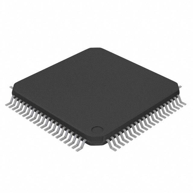


 工商网监
湘ICP备2023018690号
工商网监
湘ICP备2023018690号
