ITAxxB3
Bidirectional Transil™ array for data line protection
Features
■
High surge capability Transil array:
IPP = 40 A (8/20 µs)
■
Peak pulse power: 300 W (8/20 µs)
■
Separated Input - Output
■
Up to 9 bidirectional Transil functions
■
Low clamping factor (VCL/VBR) at high current
level
■
Low leakage current
■
ESD protection up to 15 kV
Complies with the following standards
■
■
IEC 61000-4-2 level 4
– 15 kV (air discharge)
– 8 kV (contact discharge)
MIL STD 883G- Method 3015-7: class 3B
– 25 kV (human body model)
Applications
Differential data transmission lines protection,
such as :
■
RS-232
■
RS-423
■
RS-422
■
RS-485
SO-20
Description
Transil diode arrays provide high overvoltage
protection by clamping action. Their
instantaneous response to transient overvoltages
makes them particularly suited to protect voltage
sensitive devices such as MOS technology and
low voltage supplied IC’s.
The ITA series combines high surge capability
against energetic pulses with high voltage
performance against ESD.
The separated input/output configuration of the
device ensures improved protection against very
fast transient overvoltage like ESD by elimination
of the spikes induced by parasitic inductances
created by external wiring.
Figure 1.
GND
1
20 GND
INPUT
2
19 OUTPUT
INPUT
3
18 OUTPUT
INPUT 4
17 OUTPUT
INPUT
5
16 OUTPUT
INPUT
6
15 OUTPUT
INPUT
7
14 OUTPUT
INPUT
8
13 OUTPUT
INPUT
9
12 OUTPUT
GND 10
TM: Transil is a trademark of STMicroelectronics
November 2007
Functional diagram
Rev 2
11 GND
1/8
www.st.com
8
�Characteristics
ITAxxB3
1
Characteristics
Table 1.
Absolute ratings (Tamb = 25 °C)
Symbol
PPP
IPP
Parameter
Peak pulse power (8/20 µs)(1)
Peak pulse current (8/20 µs)
Unit
Tj initial = Tamb
300
W
Tj initial = Tamb
40
A
2
I t
Wire I t value
0.6
A2s
Tj
Maximum operating junction temperature
125
°C
-55 to +150
°C
260
°C
Tstg
TL
2
(1)
Value
(1)
Storage temperature range
Maximum lead temperature for soldering during 10 s
1. For surges greater than the specified maximum value, the I/O will first present a short-circuit and after an open circuit
caused by the wire melting.
Table 2.
Electrical characteristics (Tamb = 25 °C)
Symbol
Parameter
I
IPP
VRM
Stand-off voltage
VBR
Breakdown voltage
VCL
Clamping voltage
IRM
Leakage current
IPP
Peak pulse current
αT
Voltage temperature coefficient
VF
Forward voltage drop
C
Capacitance
VBR
Order code
IRM
VRM
@ IR
min.
IRM
@
VCL
max.
@
IPP
8/20 µs
(1)
(1)
VCL
max.
@
IPP
8/20 µs
V
αT
C
max.
max.
(1)
(2)
V
mA
µA
V
V
A
V
A
10-4/°C
pF
ITA6V5B3
6.5
1
10
5
9.5
10
121
25
4
1100
ITA18B3
18
1
4
15
21
10
26
25
9
500
ITA25B3
25
1
4
24
31
10
36
25
12
420
1. Between I/O pin and ground.
2. Between two input pins at 0 V Bias, F = 1 MHz.
2/8
VRM
VCL
VBR
�ITAxxB3
Characteristics
Figure 2.
Pulse waveform
Figure 3.
Typical peak pulse power versus
exponential pulse duration
PPP(W)
%IPP
1E+04
Tj initial=25°C
ITA25B3
8 µs
100
ITA18B3
1E+03
Pulse waveform 8/20 µs
ITA6V5B3
50
1E+02
0
t
20 µs
tP(ms) expo
1E+01
1E-03
Figure 4.
Clamping voltage versus peak
pulse current (exponential
waveform 8/20 µs)
Figure 5.
VCL(V)
1E-02
1E-01
1E+00
1E+01
1E+02
Peak current IDC inducing open
circuit of the wire for one
input/output versus pulse duration
(typical values)
IDC(A)
1E+03
1E+03
%IPP
Tj initial=25°C
Exponential waveform
100
50
0
1E+02
tr
t
tp
1E+02
ITA25B3
ITA18B3
1E+01
1E+01
ITA6V5B3
IPP(A)
1E+00
1E-01
Figure 6.
1E+00
tP(ms)
1E+00
1E+01
1E-02
1E+02
Junction capacitance versus
reverse applied voltage for one
input/output (typical values)
Figure 7.
1E-01
1E+00
1E+01
Relative variation of leakage
current versus junction
temperature
IR(Tj)
IR(Tj=25°C)
C(pF)
1E+03
ITA6V5B3
Tj=25°C
F=1MHz
5E+3
1E+3
VR=VRM
1E+2
ITA18B3
1E+1
ITA25B3
1E+0
Tj(°C)
VR(V)
1E+02
1E+00
1E+01
1E+02
1E-1
0
25
50
75
100
125
150
3/8
�Application information
2
ITAxxB3
Application information
This monolithic Transil Array is based on 610 unidirectional Transils with a common cathode
and can be configurated to offer up to 9 bidirectional functions. This imposes a maximum
differential voltage between 2 input pins (see Table 3).
Table 3.
Maximum differential voltages
Order code
Maximum differential voltage between two input pins at 25°C
ITA6V5B3
± 3.5 v
ITA18B3
± 9.0 v
ITA25B3
± 12.5 v
Figure 8.
RS-232 junction (typical application)
TX
RX
RTS
CTS
DTR
DSR
CARRIER DET.
AUX
GND
2.1
Design advantage of ITAxxB3 used with 4-point structure
The ITAxxxB3 has been designed with a 4-point structure Figure 9.
The 4 point structure
(separated Input/output) to efficiently protect against
disturbances with very high di/dt rates, such as ESD.
Chip
The purpose of this 4-point structure is to eliminate the
Output 1
Input 1
overvoltage introduced by the parasitic inductances of the
BE
di/dt
wiring (Ldi/dt).
U
TO ED
T
CE EC
I
V T
GND
GND
Efficient protection depends not only on the component
DE RO
P
itself, but also on the circuit layout. The drawing given in
figure 9 shows the layout to be used in order to take
advantage of the 4-point structure of the ITAxxxB3.
With this layout, each line to be protected passes through
the protection device.
In this way, it realizes an interface between the data line
and the circuit to be protected, guaranteeing an isolation
between its inputs and outputs.
4/8
�ITAxxB3
3
Ordering information scheme
Ordering information scheme
Figure 10. Ordering information scheme
ITA
25
B
3
RL
Integrated Transil Array
Breakdown Voltage (min)
25 = 25 Volt
Type of lines protected
B = Bidirectional
Package
3 = SO-20
Packaging
RL = Tape and reel
Blank = Tube
5/8
�Package information
4
ITAxxB3
Package information
●
Epoxy meets UL94, V0
In order to meet environmental requirements, ST offers these devices in ECOPACK®
packages. These packages have a lead-free second level interconnect. The category of
second level interconnect is marked on the package and on the inner box label, in
compliance with JEDEC Standard JESD97. The maximum ratings related to soldering
conditions are also marked on the inner box label. ECOPACK is an ST trademark.
ECOPACK specifications are available at: www.st.com.
Table 4.
SO-20 dimensions
Dimensions
Ref.
Millimeters
Min.
D
hx45°
A
K
B
e
L
A1
E
H
C
Typ.
Inches
Max.
Min.
Max.
A
2.35
2.65
0.092
0.104
A1
0.10
0.30
0.004
0.008
B
0.33
0.51
0.013
0.020
C
0.23
0.32
0.009
0.013
D
12.6
13.0
0.484
0.512
E
7.40
7.60
0.291
0.299
e
1.27
0.050
H
10.0
10.65 0.394
0.419
h
0.25
0.75
0.010
0.029
L
0.40
1.27
0.016
0.050
K
8° (max)
Figure 11. SO-20 footprint (dimensions in mm)
11.2
8.5
1.27
6/8
Typ.
0.6
�ITAxxB3
5
Ordering Information
Ordering Information
Table 5.
6
Ordering information
Order code
Marking
ITA6V5B3
Package
Base qty
Delivery mode
ITA6V5B3
1000
Tube
ITA18B3
ITA18B3
1000
Tube
ITA18B3RL
ITA18B3
1000
Tape and reel
ITA25B3
ITA25B3
1000
Tube
ITA25B3RL
ITA25B3
1000
Tape and reel
SO-20
Weight
0.55 g
Revision history
Table 6.
Document revision history
Date
Revision
Changes
13-Dec-2004
1
Initial release.
07-Nov-2007
2
Reformatted to current standards. Updated leakage current values in
Table 2 Updated pulse waveform parameters in Figure 2.
7/8
�ITAxxB3
Please Read Carefully:
Information in this document is provided solely in connection with ST products. STMicroelectronics NV and its subsidiaries (“ST”) reserve the
right to make changes, corrections, modifications or improvements, to this document, and the products and services described herein at any
time, without notice.
All ST products are sold pursuant to ST’s terms and conditions of sale.
Purchasers are solely responsible for the choice, selection and use of the ST products and services described herein, and ST assumes no
liability whatsoever relating to the choice, selection or use of the ST products and services described herein.
No license, express or implied, by estoppel or otherwise, to any intellectual property rights is granted under this document. If any part of this
document refers to any third party products or services it shall not be deemed a license grant by ST for the use of such third party products
or services, or any intellectual property contained therein or considered as a warranty covering the use in any manner whatsoever of such
third party products or services or any intellectual property contained therein.
UNLESS OTHERWISE SET FORTH IN ST’S TERMS AND CONDITIONS OF SALE ST DISCLAIMS ANY EXPRESS OR IMPLIED
WARRANTY WITH RESPECT TO THE USE AND/OR SALE OF ST PRODUCTS INCLUDING WITHOUT LIMITATION IMPLIED
WARRANTIES OF MERCHANTABILITY, FITNESS FOR A PARTICULAR PURPOSE (AND THEIR EQUIVALENTS UNDER THE LAWS
OF ANY JURISDICTION), OR INFRINGEMENT OF ANY PATENT, COPYRIGHT OR OTHER INTELLECTUAL PROPERTY RIGHT.
UNLESS EXPRESSLY APPROVED IN WRITING BY AN AUTHORIZED ST REPRESENTATIVE, ST PRODUCTS ARE NOT
RECOMMENDED, AUTHORIZED OR WARRANTED FOR USE IN MILITARY, AIR CRAFT, SPACE, LIFE SAVING, OR LIFE SUSTAINING
APPLICATIONS, NOR IN PRODUCTS OR SYSTEMS WHERE FAILURE OR MALFUNCTION MAY RESULT IN PERSONAL INJURY,
DEATH, OR SEVERE PROPERTY OR ENVIRONMENTAL DAMAGE. ST PRODUCTS WHICH ARE NOT SPECIFIED AS "AUTOMOTIVE
GRADE" MAY ONLY BE USED IN AUTOMOTIVE APPLICATIONS AT USER’S OWN RISK.
Resale of ST products with provisions different from the statements and/or technical features set forth in this document shall immediately void
any warranty granted by ST for the ST product or service described herein and shall not create or extend in any manner whatsoever, any
liability of ST.
ST and the ST logo are trademarks or registered trademarks of ST in various countries.
Information in this document supersedes and replaces all information previously supplied.
The ST logo is a registered trademark of STMicroelectronics. All other names are the property of their respective owners.
© 2007 STMicroelectronics - All rights reserved
STMicroelectronics group of companies
Australia - Belgium - Brazil - Canada - China - Czech Republic - Finland - France - Germany - Hong Kong - India - Israel - Italy - Japan Malaysia - Malta - Morocco - Singapore - Spain - Sweden - Switzerland - United Kingdom - United States of America
www.st.com
8/8
�
很抱歉,暂时无法提供与“ITA6V5B3”相匹配的价格&库存,您可以联系我们找货
免费人工找货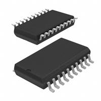


 工商网监
湘ICP备2023018690号
工商网监
湘ICP备2023018690号
