L4937N
®
DUAL MULTIFUNCTION VOLTAGE REGULATOR
.
.
.
.
..
.
.
.
.
STANDBY OUTPUT VOLTAGE PRECISION 5V
± 2%
OUTPUT 2 TRACKED TO THE STANDBY OUTPUT
OUTPUT 2 DISABLE FUNCTION FOR
STANDBY MODE
VERY LOW QUIESCENT CURRENT, LESS
THAN 250µA, IN STANDBY MODE
OUTPUT CURRENTS : I01 = 50mA, I02 = 500mA
VERY LOW DROPOUT (max 0.4V/0.6V)
OPERATING TRANSIENT SUPPLY VOLTAGE
UP TO 40V
POWER-ON RESET CIRCUIT SENSING THE
STANDBY OUTPUT VOLTAGE
POWER-ON RESET DELAY PULSE DEFINED
BY THE EXTERNAL CAPACITOR
THERMAL SHUTDOWN AND SHORT CIRCUIT
PROTECTIONS
)
s
(
t
c
u
d
o
)
r
s
(
P
t
c
e
t
u
e
d
l
o
o
r
s
P
b
e
O
t
e
l
)
o
s
(
s
t
b
c
u
O
d
o
)
r
s
P
(
t
c
e
t
u
e
l
d
o
o
r
s
P
b
O
e
t
e
l
o
s
b
O
Heptawatt
ORDERING NUMBER : L4937N
DESCRIPTION
The L4937N is a monolithic integrated dual voltage
regulators with two very low dropout outputs and additional functions such as power-on reset and input
voltage sense. It is designed for supplying microcomputer controlled systems specially in automotive applications.
PIN CONNECTION (top view)
June 2000
1/9
�L4937N
BLOCK DIAGRAM
)
s
(
t
c
u
d
o
)
r
s
(
P
t
c
e
t
u
e
d
l
o
o
r
s
P
b
e
O
t
e
l
)
o
s
(
s
t
b
c
u
O
d
o
)
r
s
P
(
t
c
e
t
u
e
l
d
o
o
r
s
P
b
O
e
t
e
l
o
s
b
O
THERMAL DATA
Symbol
Rthj-case
2/9
Parameter
Thermal Resistance Junction-Case
Max.
Value
Unit
3
°C/W
�L4937N
ABSOLUTE MAXIMUM RATINGS
Symbol
VS
Parameter
DC Supply Voltage
Transient Supply Voltage (T < 1s)
Tj, Tstg
Junction and Storage Temperature Range
Value
Unit
28
V
40
V
–55 to 150
°C
mA
IEN
Enable Input Current (VEN ≤0.3V)
±1
VEN
Enable Input Voltage
VS
VRES
Reset Output Voltage
20
V
IRES
Reset Output Current
5
mA
PD
Power Dissipation (TA = 80°C, Rth heatsink = 9°C/W)
5
W
)
s
(
t
c
u
d
o
)
r
s
(
P
t
c
e
t
u
e
d
l
o
o
r
s
P
b
e
O
t
e
l
)
o
s
(
s
t
b
c
u
O
d
o
)
r
s
P
(
t
c
e
t
u
e
l
d
o
o
r
s
P
b
O
e
t
e
l
o
s
b
O
Note : The circuit is ESD protected according to MIL–STD–883C.
APPLICATION CIRCUIT
CS ≥ 1µF ; C01 ≥ 6µF ; C02 ≥ 10µF, ESR < 10Ω at 10KHz
3/9
�L4937N
ELECTRICAL CHARACTERISTICS (VS = 14V; –40°C ≤ Tj ≤ 125°C unless otherwise specified)
Symbol
Parameter
Test Conditions
Min.
Max.
Unit
25
V
5.10
V
+25
mV
0.25
0.4
V
V
0.4
V
0.3
0.6
V
V
VS = 4.6V, IO2 = 350mA
0.6
V
Line Regulation
6V ≤ VS ≤ 25V
IO1 = 1mA; IO2 = 5mA
20
mV
VOLO1
Load Regulation 1
1mA ≤ IO1 ≤ 50mA
25
mV
VOLO2
Load Regulation 2
5mA ≤ IO2 ≤ 500mA
50
mV
ILIM1
Current Limit 1
VO1 = 4.5V
VO1 = 0V (note 2)
55
25
100
50
200
100
mA
mA
ILIM2
Current Limit 2
VO2 = 0V
550
1000
1700
mA
IQSB
Quiescent Current Standby
Mode (output 2 disabled)
IO1 = 0.3mA; TJ < 100°C
VEN ≥ 2.4V
VS = 14V
VS = 3.5V
210
340
290
850
µA
µA
30
mA
VS
Operating Supply Voltage
VO1
Standby Output Voltage
6V ≤ VS ≤ 25V
1mA ≤ IO1 ≤ 50mA
4.90
Output Voltage 2 Tracking Error
(note 1)
6V ≤ VS ≤ 25V
5mA ≤ IO2 ≤ 500mA
Enable = LOW
–25
VDP1
Dropout Voltage 1
IO1 = 10mA
IO1 = 50mA
VIO1
Input to Output Voltage
Difference in Undervoltage
Condition
VS = 4V, IO1 = 35mA
VDP2
Dropout Voltage 2
IO2 = 100mA
IO2 = 500mA
VIO2
Input to Output Voltage
Difference in Undervoltage
Condition
VOL 1.2
VO2 - VO1
Typ.
5.00
0.1
0.2
)
s
(
t
c
u
d
o
)
r
s
(
P
t
c
e
t
u
e
d
l
o
o
r
s
P
b
e
O
t
e
l
)
o
s
(
s
t
b
c
u
O
d
o
)
r
s
P
(
t
c
e
t
u
e
l
d
o
o
r
s
P
b
O
e
t
e
l
o
s
b
O
IQ
Quiescent Current
0.2
0.3
IO1 = 50mA
IO1 = 500mA
ENABLE
VENL
Enable Input LOW Voltage
(output 2 active)
–0.3
1.5
V
VENH
Enable Input HIGH Voltage
2.4
7
V
VENhyst
IEN
4/9
Enable Hysteresis
Enable Input Current
0V < VEN < 1.2V
2.5V < VEN < 7V
30
75
200
mV
–10
–1
–1.5
0
–0.5
+1
µA
µA
�L4937N
ELECTRICAL CHARACTERISTICS (continued)
RESET
Symbol
Parameter
Test Conditions
Min.
Typ.
Max.
Unit
Vo1 -0.4
4.7
Vo1 -0.1
V
50
100
200
mV
VRt
Reset Low Threshold Voltage
VRth
Reset Threshold Hysteresis
tRD
Reset Pulse Delay
CT = 100nF; tR > 100µs
55
100
180
ms
tRR
Reset Reaction Time
CT = 100nF
1
10
50
µs
0.4
V
1
µA
VS = 14V
VRL
Reset Output LOW Voltage
RRES = 10KΩ to V01 VS ≥ 1.5V
ILRES
Reset Output HIGH Leakage
VRES = 5V
VCTth
Delay Comparator Threshold
2.0
VCTth, hyst
Delay Comparator Threshold
Hysteresis
100
Note :
V
t
c
u
d
o
r
1 : VO2 connected to ADJ.VO2 can be set to higher values by inserting an external resistor divider.
2 : Foldback characteristic
P
e
(s)
mV
)
s
t(
FUNCTIONAL DESCRIPTION
The L4937N is based on the SGS-THOMSON Microelectronics modular voltage regulator approach.
Several out-standing features and auxiliary functions are provided to meet the requirements of supplying the microprocessor systems used in automotive applications.
Furthermore the device is suitable also in other applications requiring two stabilized voltages.
The modular approach allows other features and
functions to be realized easily when required.
The typical curve of the standby output voltage as
a function of the input supply voltage is shown in fig.
1.
The current consumption of the device (quiescent
current) is less than 250µA when output 2 is disabled (standby mode). The dropout voltage is controlled to reduce the quiescent current peak in the
undervoltage region and to improve the transient
response in this region.
The quiescent current is shown in fig. 2 as a function
of the supply input voltage 2.
STANDBY REGULATOR
The standby regulator uses an Isolated Collector
Vertical PNP transistor as the regulating element.
This structure allows a very low dropout voltage at
currents up to 50mA. The dropout operation of the
standby regulator is maintained down to 2V input
supply voltage. The output voltage is regulated up
to the transient input supply voltage of 40V. This feature avoids functional interruptions which could be
generated by overvoltage pulses.
OUTPUT 2 VOLTAGE
The output 2 regulator uses the same output structure as the standby regulator, but rated for an output
current of 500mA.
The output 2 regulator works in tracking mode with
the standby output voltage as a reference voltage.
The output 2 regulator can be switched off via the
Enable input.
let
o
s
b
O
)
s
(
t
c
u
d
o
r
P
e
t
e
l
o
s
b
O
r
P
e
u
d
o
)
s
(
ct
e
t
le
c
u
d
o
r
P
o
s
b
O
-
t
e
l
o
s
b
O
5/9
�L4937N
Figure 1 : Output Voltage vs. Input Voltage.
)
s
(
t
c
u
d
o
)
r
s
(
P
t
c
e
t
u
e
d
l
o
o
r
s
P
b
e
O
t
e
l
)
o
s
(
s
t
b
c
u
O
d
o
)
r
s
P
(
t
c
e
t
u
e
l
d
o
o
r
s
P
b
O
e
t
e
l
o
s
b
O
Figure 2 : Quiescent Current vs. Supply Voltage.
400
200
RESET CIRCUIT
The block circuit diagram of the reset circuit is shown
in fig. 3. The reset circuit supervises the standby output voltage. The reset threshold of 4.7V is defined
by the internal reference voltage and the standby
output divider.
The reset pulse delay time tRD, is defined by the
charge time of an external capacitor CT :
CT x 2V
tRD =
6/9
2µA
The reaction time of the reset circuit depends on the
discharge time limitation of the reset capacitor CT
and is proportional to the value of CT.
The reaction time of the reset circuit increases the
noise immunity. In fact, if the standby output voltage
drops below the reset threshold for a time shorter
than the reaction time tRR, no reset output variation
occurs. The nominal reset delay is generated for
standby output voltage drops longer than the time
necessary for the complete discharging of the capacitor CT. This time is typically equal to 50µs if CT
= 100nF. The typical reset output waveforms are
shown in fig.
�L4937N
Figure 3 : Block Diagram of the Reset Circuit.
)
s
(
t
c
u
d
o
)
r
s
(
P
t
c
e
t
u
e
d
l
o
o
r
s
P
b
e
O
t
e
l
)
o
s
(
s
t
b
c
u
O
d
o
)
r
s
P
(
t
c
e
t
u
e
l
d
o
o
r
s
P
b
O
e
t
e
l
o
s
b
O
Figure 4 : Typical Reset Output Waveforms.
VOUT1
VINPUT
VOUT1
VRT +0.2V
VRT
1.5V
tR
RESET
tRD
tRD
tRR
D95AT216
7/9
�L4937N
DIM.
A
C
D
D1
E
E1
F
F1
G
G1
G2
H2
H3
L
L1
L2
L3
L4
L5
L6
L7
L9
M
M1
V4
Dia
MIN.
mm
TYP.
2.4
1.2
0.35
0.7
0.6
2.34
4.88
7.42
2.54
5.08
7.62
MAX.
4.8
1.37
2.8
1.35
0.55
0.97
0.8
0.9
2.74
5.28
7.82
10.4
10.4
17.1
inch
TYP.
MIN.
0.094
0.047
0.014
0.028
0.024
0.095
0.193
0.295
0.100
0.200
0.300
OUTLINE AND
MECHANICAL DATA
MAX.
0.189
0.054
0.110
0.053
0.022
0.038
0.031
0.035
0.105
0.205
0.307
0.409
0.409
0.673
)
s
(
t
c
u
d
o
)
r
s
(
P
t
c
e
t
u
e
d
l
o V
o Heptawatt
r
s
P
b
e
O
t
e
l
)
o
s
(
s
t
b
c
u
O
d
o
)
r
s
P
(
t
c
e
t
u
e
l
d
o
o
r
s
P
b
O
e
t
e
l
o
s
b
O
10.05
16.7
21.24
22.27
2.6
15.1
6
2.55
4.83
16.9
14.92
21.54
22.52
2.8
15.5
6.35
0.2
2.8
5.08
3.65
21.84
22.77
1.29
3
15.8
6.6
0.396
0.657
0.386
0.877
0.102
0.594
0.236
3.05 0.100
5.33 0.190
40˚ (typ.)
3.85 0.144
0.668
0.587
0.848
0.891
0.110
0.610
0.250
0.008
0.110
0.200
0.860
0.896
0.051
0.118
0.622
0.260
0.120
0.210
0.152
V
L
V
E
L1
M1
A
M
D
C
D1
H2
L2
L5
L3
F
E
E1
V4
L9
H3
G
H1
G1
G2
Dia.
F
L4
L7
L6
8/9
H2
F1
HEPTAMEC
�L4937N
)
s
(
t
c
u
d
o
)
r
s
(
P
t
c
e
t
u
e
d
l
o
o
r
s
P
b
e
O
t
e
l
)
o
s
(
s
t
b
c
u
O
d
o
)
r
s
P
(
t
c
e
t
u
e
l
d
o
o
r
s
P
b
O
e
t
e
l
o
s
b
O
Information furnished is believed to be accurate and reliable. However, STMicroelectronics assumes no responsibility for the consequences of use of such information nor for any infringement of patents or other rights of third parties which may result from its use. No
license is granted by implication or otherwise under any patent or patent rights of STMicroelectronics. Specification mentioned in this
publication are subject to change without notice. This publication supersedes and replaces all information previously supplied. STMicroelectronics products are not authorized for use as critical components in life support devices or systems without express written
approval of STMicroelectronics.
The ST logo is a registered trademark of STMicroelectronics
© 2000 STMicroelectronics – Printed in Italy – All Rights Reserved
HEPTAWATT is a Trademark of STMicroelectronics
STMicroelectronics GROUP OF COMPANIES
Australia - Brazil - China - Finland - France - Germany - Hong Kong - India - Italy - Japan - Malaysia - Malta - Morocco Singapore - Spain - Sweden - Switzerland - United Kingdom - U.S.A.
http://www.st.com
9/9
�
很抱歉,暂时无法提供与“L4937N”相匹配的价格&库存,您可以联系我们找货
免费人工找货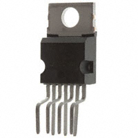


 工商网监
湘ICP备2023018690号
工商网监
湘ICP备2023018690号
