L6370Q
2.5 A single high-side smart power switch
Datasheet - production data
Applications
Programmable logic controller
Industrial PC peripheral input/output
Numerical control machines
Drivers for all loads (resistive, capacitive,
inductive load)
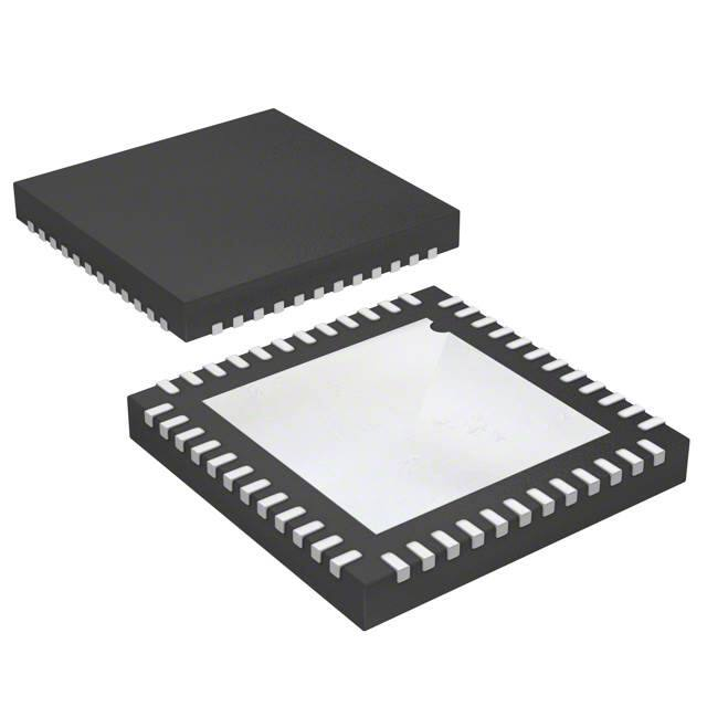
VFQFPN48
(7 x 7 mm)
Description
Features
Operating voltage range (VS) 9.5 V to 35 V
Up to Iout = 2.5 A operating current
RDS(on): 0.1 Ω
Internal current limit
The L6370Q is a monolithic intelligent power
switch in BCDmultipower technology to drive
inductive or resistive loads. An internal clamping
diode enables the fast demagnetization of
inductive loads. Diagnostic for CPU feedback and
extensive use of electrical protections make this
device extremely rugged and especially suitable
for industrial automation applications.
Thermal shutdown
Table 1. Device summary
Open ground protection
Internal negative voltage clamping for fast
demagnetization (Vdemag = Vs - 50 V)
Differential inputs with large common mode
range and threshold hysteresis
Part number
L6370Q
L6370QTR
Package
VFQFPN 7 x 7 x 1 48L
Packaging
Tube
Tape and reel
Undervoltage lockout with hysteresis
Open load detection
Two diagnostic outputs
Output status LED driver
Non-dissipative short-circuit protection
Surge and transient protection (IEC61000-4-5)
Burst transient immunity (IEC61000-4-4)
ESD protection (human body model ±2 kV)
April 2018
This is information on a product in full production.
DocID022313 Rev 3
1/17
www.st.com
�Contents
L6370Q
Contents
1
Block diagram and pin description . . . . . . . . . . . . . . . . . . . . . . . . . . . . . 3
Pin description . . . . . . . . . . . . . . . . . . . . . . . . . . . . . . . . . . . . . . . . . . . . . . . . . . . . 4
2
3
4
Electrical specifications . . . . . . . . . . . . . . . . . . . . . . . . . . . . . . . . . . . . . . 6
2.1
Absolute maximum ratings . . . . . . . . . . . . . . . . . . . . . . . . . . . . . . . . . . . . . 6
2.2
Thermal data . . . . . . . . . . . . . . . . . . . . . . . . . . . . . . . . . . . . . . . . . . . . . . . 6
2.3
Electrical characteristics . . . . . . . . . . . . . . . . . . . . . . . . . . . . . . . . . . . . . . . 7
2.4
AC operation . . . . . . . . . . . . . . . . . . . . . . . . . . . . . . . . . . . . . . . . . . . . . . . 9
Circuit description . . . . . . . . . . . . . . . . . . . . . . . . . . . . . . . . . . . . . . . . . . 10
3.1
Diagnostic truth table . . . . . . . . . . . . . . . . . . . . . . . . . . . . . . . . . . . . . . . . .11
3.2
Input section . . . . . . . . . . . . . . . . . . . . . . . . . . . . . . . . . . . . . . . . . . . . . . . .11
3.3
Diagnostic logic . . . . . . . . . . . . . . . . . . . . . . . . . . . . . . . . . . . . . . . . . . . . .11
3.4
Short-circuit operation . . . . . . . . . . . . . . . . . . . . . . . . . . . . . . . . . . . . . . . 12
3.5
Overtemperature protection (OVT) . . . . . . . . . . . . . . . . . . . . . . . . . . . . . . 12
3.6
Undervoltage protection (UV) . . . . . . . . . . . . . . . . . . . . . . . . . . . . . . . . . . 12
3.7
Demagnetization of inductive loads . . . . . . . . . . . . . . . . . . . . . . . . . . . . . 13
Package information . . . . . . . . . . . . . . . . . . . . . . . . . . . . . . . . . . . . . . . . 14
4.1
5
2/17
VFQFPN48 (7 x 7 x 1.0 mm) package information . . . . . . . . . . . . . . . . . 14
Revision history . . . . . . . . . . . . . . . . . . . . . . . . . . . . . . . . . . . . . . . . . . . 16
DocID022313 Rev 3
�L6370Q
Block diagram and pin description
Figure 1.Block diagram
VS
UNDER
VOLTAGE
IN+
INPUT
IN-
CHARGE
PUMP
+
DRIVER
1.4V
OUT
NON DISSIPATIVE
SHORT CIRCUIT
ON-DELAY
CURRENT
LIMITATION
RSC
OPEN LOAD
DETECTION
OSC
OUTSTATUS
DIAG1
DIAGNOSTIC
THERMAL
PROTECTION
DIAG2
3mA
OUTPUT STATUS
D95IN208D
��
287387
1&
28767$786
1&
1&
*1'
1&
1&
1&
1&
1&
1&
1&
Figure 2. Pin connections (top view)
��
�
��
1&
287387
1&
1&
,1�
21�'(/$<
,1�
9V
1&
9V
1&
9V
1&
9V
',$*��
1&
',$*��
1&
287387
1&
287387
��
��
1&
DocID022313 Rev 3
1&
1&
1&
56&
1&
1&
1&
1&
1&
��
1&
��
1&
1&
1&
1
Block diagram and pin description
3/17
17
�Block diagram and pin description
L6370Q
Pin description
Table 2. Pin description
4/17
Pin
Name
Description
1
OUTPUT
High-side output with built-in current limitation
2
OUTPUT
High-side output with built-in current limitation
3
NC
4
ON-DELAY
5
VS
Supply voltage input, the value of the supply voltage is monitored to detect
undervoltage conditions
6
VS
Supply voltage input, the value of the supply voltage is monitored to detect
undervoltage conditions
7
VS
Supply voltage input, the value of the supply voltage is monitored to detect
undervoltage conditions
8
VS
Supply voltage input, the value of the supply voltage is monitored to detect
undervoltage conditions
9
NC
Not connected
10
OUTPUT
High-side output with built-in current limitation
11
OUTPUT
High-side output with built-in current limitation
12
NC
Not connected
13
NC
Not connected
14
NC
Not connected
15
NC
Not connected
16
NC
Not connected
17
NC
Not connected
18
NC
Not connected
19
NC
Not connected
20
NC
Not connected
21
NC
Not connected
22
RSC
23
NC
Not connected
24
NC
Not connected
25
NC
Not connected
26
NC
Not connected
27
NC
Not connected
28
DIAG1
DIAGNOSTIC1 output. This open drain reports the IC working
conditions (see Table 6 on page 9).
29
DIAG2
DIAGNOSTIC2 output. This open drain reports the IC working conditions (see
Table 6).
Not connected
Programmable on-time interval duration during short-circuit operation
Current limitation settings
DocID022313 Rev 3
�L6370Q
Block diagram and pin description
Table 2. Pin description (continued)
Pin
Name
Description
30
NC
Not connected
31
NC
Not connected
32
NC
Not connected
33
IN+
Comparator inverting input
34
IN-
Comparator non-inverting input
35
NC
Not connected
36
NC
Not connected
37
NC
Not connected
38
OUTSTATUS
39
NC
Not connected
40
NC
Not connected
41
GND
42
NC
Not connected
43
NC
Not connected
44
NC
Not connected
45
NC
Not connected
46
NC
Not connected
47
NC
Not connected
48
NC
Not connected
This current source output drives a LED to signal the status of the output pin.
The pin is active (source current) when the output pin is considered high.
Ground
DocID022313 Rev 3
5/17
17
�Electrical specifications
L6370Q
2
Electrical specifications
2.1
Absolute maximum ratings
Table 3. Absolute maximum ratings
Symbol
VS
VS - Vo
Value
Unit
50
V
Internally limited
V
Supply voltage (Tw < 10 ms)
Supply to output differential voltage (see also Vcl)
Vod
Externally forced voltage
-0.3 to 7
V
Iod
Externally forced current
±1
mA
VIN
Input voltage
-10 to Vs+10
V
Vi
Differential input voltage
43
V
IIN
Input current
20
mA
Iout
Output current (see also Isc)
Internally limited
A
EAS
Single pulse avalanche energy
(Tamb = 125 °C, VCC = 24 V, Iload = 2.0 A)
6.0
J
PTOT
Power dissipation (see also thermal characteristics)
Internally limited
W
Operating temperature range
-40 to +105
°C
Storage temperature
-55 to 150
°C
Top
TSTG
2.2
Parameter
Thermal data
Table 4. Thermal data
Symbol
Rth(JC)
Rth(JA)
Description
Value
Thermal resistance junction-case
Thermal resistance junction-ambient
(1)
Max.
4
Max.
50
1. Mounted on a 2-side + vias PCB with a ground dissipating area on the bottom side.
6/17
DocID022313 Rev 3
Unit
°C/W
�L6370Q
2.3
Electrical specifications
Electrical characteristics
(Vs = 24 V; TJ = –25 to +125 °C, unless otherwise specified)
Table 5. Electrical characteristics
Symbol
Parameter
Test conditions
Min.
Typ.
Max.
Unit
4
-
35
V
9.5
24
35
V
-
0.8
3
1.4
4
mA
8.5
9
9.5
V
Supply voltage for valid diagnostics
Idiag> 0.5 mA; Vdg1= 1.5 V
Vs
Supply voltage (operative)
-
Iq
Quiescent current Iout = Ios = 0
Vil
Vih
Vsth1
Undervoltage threshold 1
Tamb = 0 to +85 °C
(see Figure 4)
Vsth2
Undervoltage threshold 2
-
8
8.5
9
V
Vsth3
Supply voltage hysteresis
-
300
500
700
mV
Short-circuit current
Vs = 9.5 to 35 V; RL= 2 Ω
5 kΩ < RSC< 30 kΩ
Vsmin
Isc
15/RSC(kΩ)
0< RSC< 5 kΩ
Vdon
Output voltage drop
A
2.6
3.2
4
A
Iout = 2.0 A, Tj = 25 °C
Tj = 125 °C
-
200
320
280
440
mV
Iout = 2.5 A, Tj = 25 °C
Tj = 125 °C
-
250
400
350
550
mV
Ioslk
Output leakage current
Vi = Vil; Vo = 0 V
-
-
500
μA
Vol
Low-state out voltage
Vi = Vil; RL =
-
0.8
1.5
V
Vcl
Internal voltage clamp
(Vs - VO)
IO = 1 A
Single pulsed: Tp = 300 μs
48
53
58
V
Iold
Open load detection current
Vi = Vih; Tamb = 0 to + 85 °C
1
3
6
mA
Vid
Common mode input voltage range
(operative)
Vs = 18 to 35 V
-7
-
15
V
Iib
Input bias current
Vi = -7 to 15 V; -In = 0 V
-250
-
250
μA
Vith
Input threshold voltage
V +In > V -In
0.8
1.4
2
V
Viths
Input threshold hysteresis voltage
V +In > V -In
50
-
400
mV
Rid
Differential input resistance
0 < +In < +16 V; -In = 0 V
-7 < +In < 0 V; -In = 0 V
-
400
150
-
kΩ
Iilk
Input offset current
V +In = V -In
0 V < Vi < 5.5 V
+Ii
-Ii
-20
-75
-25
-In = GND
0 V < V + In V - In).
DocID022313 Rev 3
�L6370Q
2.4
Electrical specifications
AC operation
Table 6. AC operation
Symbol
Test conditions
Min.
Typ.
Max.
Unit
Rise or fall time
Vs = 24 V; RI = 70 Ω; Rl to ground
-
20
-
μs
Delay time
-
-
5
-
μs
Slew rate (rise and fall edge)
-
0.7
1
1.5
V/μs
tON
On-time during short-circuit condition
50 pF < CON < 2 nF
-
1.28
-
μs/pF
tOFF
Off-time during short-circuit condition
-
-
64
-
tON
fmax
Maximum operating frequency
-
-
25
-
kHz
tr - tf
td
dV/dt
Parameter
DocID022313 Rev 3
9/17
17
�Circuit description
3
L6370Q
Circuit description
Figure 3. Output status hysteresis
Vohys
Voth1
Voth2
D95IN211A
VOUT
Figure 4. Undervoltage comparator hysteresis
Vsth3
Vsth1
Vsth2
D95IN212
Vs
Figure 5. Switching waveforms
Vin
50%
50%
td
t
td
Vout
90%
90%
50%
50%
10%
10%
tr
10/17
DocID022313 Rev 3
tf
D94IN127A
t
�L6370Q
3.1
Circuit description
Diagnostic truth table
Table 7. Diagnostic truth table
Diagnostic conditions
Input
Output
Diag1
Diag2
Normal operation
L
H
L
H
H
H
H
H
Open load condition (Io< Iold)
L
H
L
H
H
L
H
H
Short to Vs
L
H
H
H
L
L
H
H
Short-circuit to ground (IO = ISC) (1)
(ON-DELAY pin grounded)
H
L
X
L
H
H
H
H
Output DMOS open
L
H
L
L
H
L
H
H
Overtemperature
L
H
L
L
H
H
L
L
Supply undervoltage (Vs< Vsth2)
L
H
L
L
L
L
L
L
1. A cold lamp filament, or a capacitive load may activate the current limiting circuit of the IPS, when the IPS
is initially turned on.
3.2
Input section
The input section is a high impedance differential stage with high common and differential
mode range. Built-in offset of +1.4 V (typical value) and a hysteresis of 400 mV (maximum
value) assure high noise immunity.
3.3
Diagnostic logic
The operating conditions of the device are permanently monitored and the following
occurrences are indicated by DIAG1/DIAG2 open drain output pins:
Short-circuit versus ground. A current limit circuit fixes Isc = 3.2 A (typical value) the
maximum current that can be sourced from the OUTPUT pin (for more details see
Section 3.4: Short-circuit operation)
Short-circuit versus Vs
Undervoltage (UV)
Overtemperature (OVT)
Open load, if the output current is less than 3 mA (typical value)
Output DMOS open according to Table 7
DocID022313 Rev 3
11/17
17
�Circuit description
3.4
L6370Q
Short-circuit operation
In order to minimize the power dissipation when the output is shorted-to-ground, an
innovative, non-dissipative short-circuit protection (patent pending) is implemented,
avoiding the thermal protection.
Whenever the output is shorted-to-ground, or, an overcurrent is sinked by the load, the
output devices are driven to linear mode, sourcing the Isc current (3.2 A typ.) for a time
interval (tON) defined by the external CON capacitor connected between the ON-DELAY pin
and GND. If the short-circuit increases within the tON interval the DIAG2 output status is not
affected, acting as a programmable diagnostic delay.
This function allows the device to drive a capacitive load or a filament lamp (that exhibits a
very low resistance during the initial heading phase) without the diagnostic. If the shortcircuit lasts for the whole tON interval, the output DMOS is switched off and the DIAG2 goes
low, for a time interval tOFF lasting tON 64 times.
At the end of the tOFF interval if the short-circuit condition is still present, the output DMOS is
turned on (and the DIAG2 goes high - see Figure 7) for another tON interval and the
sequence starts again, otherwise, the normal condition operation is resumed.
The tON interval can be set to last between 64 ms and 2.56 ms for a CON capacitor value
ranging between 50 pF and 2 nF:
Equation 1
tON (μs) = 1.28 CON (pF)
If the ON-DELAY pin is grounded, the non-dissipative short-circuit protection is disabled and
the Isc current is delivered until the overtemperature protection shuts the device off. The
behavior of the DIAG2 output is, in this situation, showed in Table 7.
3.5
Overtemperature protection (OVT)
If the chip temperature exceeds lim (measured in a central position in the chip) the chip
deactivates itself.
The following actions are taken:
the output stage is switched off
the signal DIAG2 is activated (active low)
Normal operation is resumed as soon as (after some seconds) the chip temperature
monitored goes back below lim-th.
The different thresholds with hysteretic behavior assure that any intermittent condition can
be generated.
3.6
Undervoltage protection (UV)
The supply voltage is expected to range from 9.5 V to 35 V, even if its reference value is
24 V.
In this range, the device operates correctly. Below 9.5 V the overall system is not reliable.
12/17
DocID022313 Rev 3
�L6370Q
Circuit description
Protection shuts off the output whenever the supply voltage falls below the mask fixed by
Vsth1(9 V typ.) and Vsth2 (8.5 V typ.).
The hysteresis (see Figure 4) assures a non-intermittent behavior at low supply voltage with
a superimposed ripple. The undervoltage status is indicated by the DIAG1 and DIAG2
outputs (see Table 7).
3.7
Demagnetization of inductive loads
An internal Zener diode, limiting the voltage across the power MOSFET between 50 and
60 V (Vcl), provides safe and fast demagnetization of inductive loads without external
clamping devices. The maximum energy that can be absorbed by an inductive load is
specified in Table 3.
Figure 6. L6370Q short-circuit operation waveforms
Figure 7. Inductive load equivalent circuit
+VS
IS
50V
VS
OUTPUT
IO
L
RL
D95IN215A
DocID022313 Rev 3
13/17
17
�Package information
4
L6370Q
Package information
In order to meet environmental requirements, ST offers these devices in different grades of
ECOPACK® packages, depending on their level of environmental compliance. ECOPACK®
specifications, grade definitions and product status are available at: www.st.com.
ECOPACK® is an ST trademark.
4.1
VFQFPN48 (7 x 7 x 1.0 mm) package information
Figure 8. VFQFPN48 (7 x 7 x 1.0 mm) package outline
14/17
DocID022313 Rev 3
�L6370Q
Package information
Table 8. VFQFPN48 (7 x 7 x 1.0 mm) package mechanical data
Dimensions (mm)
Symbol
Min.
Typ.
Max.
A
0.80
0.90
1.00
A1
-
0.02
0.05
A2
-
0.65
1.00
A3
-
0.25
-
b
0.18
0.23
0.30
D
6.85
7.00
7.15
D2
4.95
5.10
5.25
E
6.85
7.00
7.15
E2
4.95
5.10
5.25
e
0.45
0.50
0.55
L
0.30
0.40
0.50
ddd
-
0.08
-
DocID022313 Rev 3
15/17
17
�Revision history
5
L6370Q
Revision history
Table 9. Document revision history
16/17
Date
Revision
Changes
04-Oct-2011
1
Initial release.
24-Jan-2013
2
Changed the operating temperature range parameter in
Table 3.
Minor text changes.
06-Apr-2018
3
Updated Table 3 (replaced Ei by EAS symbol, updated
parameter and value).
Minor modifications throughout document.
DocID022313 Rev 3
�L6370Q
IMPORTANT NOTICE – PLEASE READ CAREFULLY
STMicroelectronics NV and its subsidiaries (“ST”) reserve the right to make changes, corrections, enhancements, modifications, and
improvements to ST products and/or to this document at any time without notice. Purchasers should obtain the latest relevant information on
ST products before placing orders. ST products are sold pursuant to ST’s terms and conditions of sale in place at the time of order
acknowledgement.
Purchasers are solely responsible for the choice, selection, and use of ST products and ST assumes no liability for application assistance or
the design of Purchasers’ products.
No license, express or implied, to any intellectual property right is granted by ST herein.
Resale of ST products with provisions different from the information set forth herein shall void any warranty granted by ST for such product.
ST and the ST logo are trademarks of ST. All other product or service names are the property of their respective owners.
Information in this document supersedes and replaces information previously supplied in any prior versions of this document.
© 2018 STMicroelectronics – All rights reserved
DocID022313 Rev 3
17/17
17
�


 工商网监
湘ICP备2023018690号
工商网监
湘ICP备2023018690号
