LD29080 SERIES
800mA FIXED AND ADJUSTABLE OUTPUT VERY LOW DROP VOLTAGE REGULATOR
PRELIMINARY DATA
s
s
s
s s
VERY LOW DROPOUT VOLTAGE (TYP. 0.4V AT 800mA) GUARANTEED OUTPUT CURRENT UP TO 800mA FIXED AND ADJUSTABLE OUTPUT VOLTAGE (±1% AT 25°C) INTERNAL CURRENT AND THERMAL LIMIT LOGIC CONTROLLED ELECTRONIC SHUTDOWN
PPAK
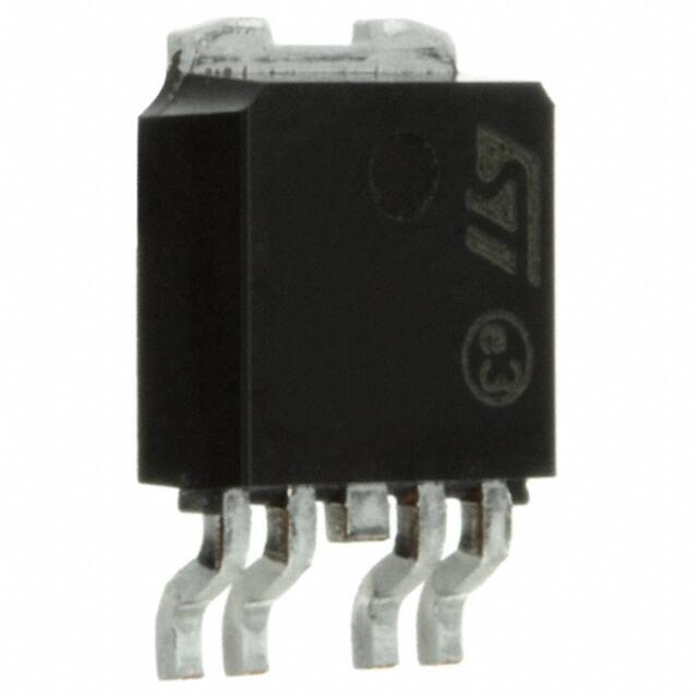
DPAK
DESCRIPTION The LD29080 is a high current, high accuracy, low-dropout voltage regulators series. These regulators feature 400mV dropout voltages and very low ground current. Designed for high current loads, these devices also find applications in lower current, extremely low dropout-critical systems, where their tiny dropout voltage and ground current values are important attributes. Typical application are in Power supply switching post
SOT-223
regulation, Series power supply for monitors, Series power supply for VCRs and TVs, Computer Systems and Battery powered systems.
Figure 1: Schematic Diagram For Adjustable Version
October 2004
Rev. 1
1/21
This is preliminary information on a new product now in development or undergoing evaluation. Details are subject to change without notice.
�LD29080 SERIES
Figure 2: Schematic Diagram For Fixed Version
Table 1: Ordering Codes
DPAK (*) LD29080DT15 LD29080DT18 LD29080DT25 LD29080DT33 LD29080DT50 LD29080DT80 LD29080DT90 PPAK (*) LD29080PT15 LD29080PT18 LD29080PT25 LD29080PT33 LD29080PT50 LD29080PT80 LD29080PT90 LD29080PT SOT-223 LD29080S15 LD29080S18 LD29080S25 LD29080S33 LD29080S50 LD29080S80 LD29080S90 OUTPUT VOLTAGE 1.5 V 1.8 V 2.5 V 3.3 V 5.0 V 8.0 V (**) 9.0 V (**) ADJ
(*) Available in Tape & Reel with the suffix "R", for the adj version "-R" (**) Available on Request
Table 2: Absolute Maximum Ratings
Symbol VI VINH IO PD Tstg Top DC Input Voltage Inhibit Input Voltage Output Current Power Dissipation Storage Temperature Range Storage Temperature Range Parameter Value 30 (*) 14 Internally Limited Internally Limited -55 to 150 -40 to 125 Unit V V mA mW °C °C
(*) Above 14V the device is automatically in shut-down. Absolute Maximum Ratings are those beyond which damage to the device may occur. Functional operation under these condition is not implied.
2/21
�LD29080 SERIES
Table 3: Thermal Data
Symbol Rthj-case Rthj-amb Parameter Thermal Resistance Junction-case Thermal Resistance Junction-ambient DPAK 8 100 PPAK 8 100 SOT-223 15 Unit °C/W °C/W
Figure 3: Pin Connection (top view)
PPAK
DPAK
SOT-223 Table 4: Pin Description
Symbol VI GND VO ADJ/N.C.** INHIBIT* PPAK 2 3 4 5 1 DPAK 1 2 3 SOT-223 1 2 3
* Not internally pulled up; in order to assure the operating condition (device in ON mode), it must be connected to a positive voltage higher than 2V. ** Not connect for fixed version.
3/21
�LD29080 SERIES
Figure 4: Application Circuit
R VO = VREF (1 + 1 ) R2
* Only for version with inhibit function.
Table 5: Electrical Characteristics Of LD29080#15 (IO = 10mA (Note 4), TJ = 25°C, VI = 3.5V, VINH = 2V, CI = 330nF, CO = 10µF, unless otherwise specified)
Symbol VI VO ∆VO ∆VO SVR Iq Parameter Operating Input Voltage Output Voltage Load Regulation Line Regulation Supply Voltage Rejection Quiescent Current Test Conditions IO = 10mA to 800mA IO = 10mA to 800mA, VI = 3 to 7V TJ = -40 to 125°C IO = 10mA to 800mA VI = 3 to 13V f = 120 Hz, VI = 3.5 ± 1V, IO = 400mA (Note 1) IO = 10mA, TJ = -40 to 125°C IO = 400mA, IO = 800mA, VI = 13V, VINH = GND Isc VIL VIH IINH eN Short Circuit Current Control Input Logic Low Control Input Logic High Control Input Current Output Noise Voltage RL = 0 OFF MODE ON MODE VINH = 13V TJ = -40 to 125°C TJ = -40 to 125°C TJ = -40 to 125°C 2 5 60 10 TJ = -40 to 125°C TJ = -40 to 125°C TJ = -40 to 125°C 65 Min. 2.5 1.485 1.463 1.5 0.2 0.06 75 2 8 14 130 1.2 0.8 5 20 35 180 µA A V V µA µVRMS Typ. Max. 13 1.515 1.537 1.0 0.5 Unit V V % % dB mA
BP = 10Hz to 100KHzIO = 100mA
NOTE 1: Guaranteed by design. NOTE 2: Dropout voltage is defined as the input-to-output differential when the output voltage drops to 99% of its nominal value with VO+1V applied to VI. NOTE 3: Reference Voltage is measured between output and GND pins, with ADJ PIN tied to VOUT. NOTE 4: in order to avoid any output voltage rise within the whole operating temperature range, due to output leakage current, a minimum load current of 2mA is required.
4/21
�LD29080 SERIES
Table 6: Electrical Characteristics Of LD29080#18 (IO = 10mA (Note 4), TJ = 25°C, VI = 3.5V, VINH = 2V, CI = 330nF, CO = 10µF, unless otherwise specified)
Symbol VI VO ∆VO ∆VO SVR VDROP Parameter Operating Input Voltage Output Voltage Load Regulation Line Regulation Supply Voltage Rejection Dropout Voltage Test Conditions IO = 10mA to 800mA IO = 10mA to 800mA, VI = 3 to 7.3V TJ = -40 to 125°C IO = 10mA to 800mA VI = 3 to 13V f = 120 Hz, VI = 3.8 ± 1V, IO = 400mA (Note 1) IO = 150mA,TJ = -40 to 125°C (Note 2) IO = 400mA,TJ = -40 to 125°C (Note 2) IO = 800mA,TJ = -40 to 125°C (Note 2) Iq Quiescent Current IO = 10mA, IO = 400mA, IO = 800mA, VI = 13V, VINH = GND Isc VIL VIH IINH eN Short Circuit Current Control Input Logic Low Control Input Logic High Control Input Current Output Noise Voltage RL = 0 OFF MODE ON MODE VINH = 13V TJ = -40 to 125°C TJ = -40 to 125°C TJ = -40 to 125°C 2 5 72 10 TJ = -40 to 125°C TJ = -40 to 125°C TJ = -40 to 125°C TJ = -40 to 125°C 62 Min. 2.5 1.782 1.755 1.8 0.2 0.06 72 0.1 0.2 0.4 2 8 14 130 1.2 0.8 0.7 5 20 35 180 µA A V V µA µVRMS mA Typ. Max. 13 1.818 1.845 1.0 0.5 Unit V V % % dB V
BP = 10Hz to 100KHzIO = 100mA
NOTE 1: Guaranteed by design. NOTE 2: Dropout voltage is defined as the input-to-output differential when the output voltage drops to 99% of its nominal value with VO+1V applied to VI. NOTE 3: Reference Voltage is measured between output and GND pins, with ADJ PIN tied to VOUT. NOTE 4: in order to avoid any output voltage rise within the whole operating temperature range, due to output leakage current, a minimum load current of 2mA is required.
5/21
�LD29080 SERIES
Table 7: Electrical Characteristics Of LD29080#25 (IO = 10mA (Note 4), TJ = 25°C, VI = 4.5V, VINH = 2V, CI = 330nF, CO = 10µF, unless otherwise specified)
Symbol VI VO ∆VO ∆VO SVR VDROP Parameter Operating Input Voltage Output Voltage Load Regulation Line Regulation Supply Voltage Rejection Dropout Voltage Test Conditions IO = 10mA to 800mA IO = 10mA to 800mA, VI = 3.5 to 8V TJ = -40 to 125°C IO = 10mA to 800mA VI = 3.5 to 13V f = 120 Hz, VI = 4.5 ± 1V, IO = 400mA (Note 1) IO = 150mA,TJ = -40 to 125°C (Note 2) IO = 400mA,TJ = -40 to 125°C (Note 2) IO = 800mA,TJ = -40 to 125°C (Note 2) Iq Quiescent Current IO = 10mA, IO = 400mA, IO = 800mA, VI = 13V, VINH = GND Isc VIL VIH IINH eN Short Circuit Current Control Input Logic Low Control Input Logic High Control Input Current Output Noise Voltage RL = 0 OFF MODE ON MODE VINH = 13V TJ = -40 to 125°C TJ = -40 to 125°C TJ = -40 to 125°C 2 5 100 10 TJ = -40 to 125°C TJ = -40 to 125°C TJ = -40 to 125°C TJ = -40 to 125°C 55 2.475 2.438 2.5 0.2 0.06 70 0.1 0.2 0.4 2 8 14 130 1.2 0.8 0.7 5 20 35 180 µA A V V µA µVRMS mA Min. Typ. Max. 13 2.525 2.562 1.0 0.5 Unit V V % % dB V
BP = 10Hz to 100KHzIO = 100mA
NOTE 1: Guaranteed by design. NOTE 2: Dropout voltage is defined as the input-to-output differential when the output voltage drops to 99% of its nominal value with VO+1V applied to VI. NOTE 3: Reference Voltage is measured between output and GND pins, with ADJ PIN tied to VOUT. NOTE 4: in order to avoid any output voltage rise within the whole operating temperature range, due to output leakage current, a minimum load current of 2mA is required.
6/21
�LD29080 SERIES
Table 8: Electrical Characteristics Of LD29080#33 (IO = 10mA (Note 4), TJ = 25°C, VI = 5.3V, VINH = 2V, CI = 330nF, CO = 10µF, unless otherwise specified)
Symbol VI VO ∆VO ∆VO SVR VDROP Parameter Operating Input Voltage Output Voltage Load Regulation Line Regulation Supply Voltage Rejection Dropout Voltage Test Conditions IO = 10mA to 800mA IO = 10mA to 800mA, VI = 4.3 to 8.8V TJ = -40 to 125°C IO = 10mA to 800mA VI = 4.3 to 13V f = 120 Hz, VI = 5.3 ± 1V, IO = 400mA (Note 1) IO = 150mA,TJ = -40 to 125°C (Note 2) IO = 400mA,TJ = -40 to 125°C (Note 2) IO = 800mA,TJ = -40 to 125°C (Note 2) Iq Quiescent Current IO = 10mA, IO = 400mA, IO = 800mA, VI = 13V, VINH = GND Isc VIL VIH IINH eN Short Circuit Current Control Input Logic Low Control Input Logic High Control Input Current Output Noise Voltage RL = 0 OFF MODE ON MODE VINH = 13V TJ = -40 to 125°C TJ = -40 to 125°C TJ = -40 to 125°C 2 5 132 10 TJ = -40 to 125°C TJ = -40 to 125°C TJ = -40 to 125°C TJ = -40 to 125°C 52 3.267 3.218 3.3 0.2 0.06 67 0.1 0.2 0.4 2 8 14 130 1.2 0.8 0.7 5 20 35 180 µA A V V µA µVRMS mA Min. Typ. Max. 13 3.333 3.382 1.0 0.5 Unit V V % % dB V
BP = 10Hz to 100KHzIO = 100mA
NOTE 1: Guaranteed by design. NOTE 2: Dropout voltage is defined as the input-to-output differential when the output voltage drops to 99% of its nominal value with VO+1V applied to VI. NOTE 3: Reference Voltage is measured between output and GND pins, with ADJ PIN tied to VOUT. NOTE 4: in order to avoid any output voltage rise within the whole operating temperature range, due to output leakage current, a minimum load current of 2mA is required.
7/21
�LD29080 SERIES
Table 9: Electrical Characteristics Of LD29080#50 (IO = 10mA (Note 4), TJ = 25°C, VI = 7V, VINH = 2V, C I = 330nF, CO = 10µF, unless otherwise specified)
Symbol VI VO ∆VO ∆VO SVR VDROP Parameter Operating Input Voltage Output Voltage Load Regulation Line Regulation Supply Voltage Rejection Dropout Voltage Test Conditions IO = 10mA to 800mA IO = 10mA to 800mA, VI = 6 to 10.5V TJ = -40 to 125°C IO = 10mA to 800mA VI = 6 to 13V f = 120 Hz, VI = 7 ± 1V, IO = 400mA (Note 1) IO = 150mA,TJ = -40 to 125°C (Note 2) IO = 400mA,TJ = -40 to 125°C (Note 2) IO = 800mA,TJ = -40 to 125°C (Note 2) Iq Quiescent Current IO = 10mA, IO = 400mA, IO = 800mA, Isc VIL VIH IINH eN Short Circuit Current Control Input Logic Low Control Input Logic High Control Input Current Output Noise Voltage TJ = -40 to 125°C TJ = -40 to 125°C TJ = -40 to 125°C 49 4.95 4.875 5 0.2 0.06 64 0.1 0.2 0.4 2 8 14 130 1.2 0.8 2 5 320 10 0.7 5 20 35 180 µA A V V µA µVRMS mA Min. Typ. Max. 13 5.05 5.125 1.0 0.5 Unit V V % % dB V
VI = 13V, VINH = GND TJ = -40 to 125°C RL = 0 OFF MODE ON MODE VINH = 13V TJ = -40 to 125°C TJ = -40 to 125°C TJ = -40 to 125°C
BP = 10Hz to 100KHzIO = 100mA
NOTE 1: Guaranteed by design. NOTE 2: Dropout voltage is defined as the input-to-output differential when the output voltage drops to 99% of its nominal value with VO+1V applied to VI. NOTE 3: Reference Voltage is measured between output and GND pins, with ADJ PIN tied to VOUT. NOTE 4: in order to avoid any output voltage rise within the whole operating temperature range, due to output leakage current, a minimum load current of 2mA is required.
8/21
�LD29080 SERIES
Table 10: Electrical Characteristics Of LD29080#80 (IO = 10mA (Note 4), TJ = 25°C, VI = 10V, VINH = 2V, CI = 330nF, CO = 10µF, unless otherwise specified)
Symbol VI VO ∆VO ∆VO SVR VDROP Parameter Operating Input Voltage Output Voltage Load Regulation Line Regulation Supply Voltage Rejection Dropout Voltage Test Conditions IO = 10mA to 800mA IO = 10mA to 800mA, VI = 9 to 13V TJ = -40 to 125°C IO = 10mA to 800mA VI = 9 to 13V f = 120 Hz, VI = 9 ± 1V, IO = 400mA (Note 1) IO = 150mA,TJ = -40 to 125°C (Note 2) IO = 400mA,TJ = -40 to 125°C (Note 2) IO = 800mA,TJ = -40 to 125°C (Note 2) Iq Quiescent Current IO = 10mA, IO = 400mA, IO = 800mA, VI = 13V, VINH = GND Isc VIL VIH IINH eN Short Circuit Current Control Input Logic Low Control Input Logic High Control Input Current Output Noise Voltage RL = 0 OFF MODE ON MODE VINH = 13V TJ = -40 to 125°C TJ = -40 to 125°C TJ = -40 to 125°C 2 5 320 10 TJ = -40 to 125°C TJ = -40 to 125°C TJ = -40 to 125°C TJ = -40 to 125°C 45 7.92 7.80 8 0.2 0.06 59 0.1 0.2 0.4 2 8 14 130 1.2 0.8 0.7 5 20 35 180 µA A V V µA µVRMS mA Min. Typ. Max. 13 8.08 8.20 1.0 0.5 Unit V V % % dB V
BP = 10Hz to 100KHzIO = 100mA
NOTE 1: Guaranteed by design. NOTE 2: Dropout voltage is defined as the input-to-output differential when the output voltage drops to 99% of its nominal value with VO+1V applied to VI. NOTE 3: Reference Voltage is measured between output and GND pins, with ADJ PIN tied to VOUT. NOTE 4: in order to avoid any output voltage rise within the whole operating temperature range, due to output leakage current, a minimum load current of 2mA is required.
9/21
�LD29080 SERIES
Table 11: Electrical Characteristics Of LD29080#90 (IO = 10mA (Note 4), TJ = 25°C, VI = 11V, VINH = 2V, CI = 330nF, C O = 10µF, unless otherwise specified)
Symbol VI VO ∆VO ∆VO SVR VDROP Parameter Operating Input Voltage Output Voltage Load Regulation Line Regulation Supply Voltage Rejection Dropout Voltage Test Conditions IO = 10mA to 800mA IO = 10mA to 800mA, VI = 10 to 13V TJ = -40 to 125°C IO = 10mA to 800mA VI = 10 to 13V f = 120 Hz, VI = 11 ± 1V, IO = 400mA (Note 1) IO = 150mA,TJ = -40 to 125°C (Note 2) IO = 400mA,TJ = -40 to 125°C (Note 2) IO = 800mA,TJ = -40 to 125°C (Note 2) Iq Quiescent Current IO = 10mA, IO = 400mA, IO = 800mA, Isc VIL VIH IINH eN Short Circuit Current Control Input Logic Low Control Input Logic High Control Input Current Output Noise Voltage TJ = -40 to 125°C TJ = -40 to 125°C TJ = -40 to 125°C 45 8.91 8.775 9 0.2 0.06 58 0.1 0.2 0.4 2 8 14 130 1.2 0.8 2 5 360 10 0.7 5 20 35 180 µA A V V µA µVRMS mA Min. Typ. Max. 13 9.09 9.225 1.0 0.5 Unit V V % % dB V
VI = 13V, VINH = GND TJ = -40 to 125°C RL = 0 OFF MODE ON MODE VINH = 13V TJ = -40 to 125°C TJ = -40 to 125°C TJ = -40 to 125°C
BP = 10Hz to 100KHzIO = 100mA
NOTE 1: Guaranteed by design. NOTE 2: Dropout voltage is defined as the input-to-output differential when the output voltage drops to 99% of its nominal value with VO+1V applied to VI. NOTE 3: Reference Voltage is measured between output and GND pins, with ADJ PIN tied to VOUT. NOTE 4: in order to avoid any output voltage rise within the whole operating temperature range, due to output leakage current, a minimum load current of 2mA is required.
10/21
�LD29080 SERIES
Table 12: Electrical Characteristics Of LD29080#ADJ (IO = 10mA (Note 4), TJ = 25°C, VI = 3.23 V, VINH = 2V, CI = 330nF, C O = 10µF adjust pin tied to output pin, unless otherwise specified)
Symbol VI ∆VO ∆VO VREF SVR Iq Parameter Minimum Operating Input Voltage Load Regulation Line Regulation Reference Voltage Supply Voltage Rejection Quiescent Current Test Conditions IO = 10mA to 800mA IO = 10mA to 800mA VI = 2.5 V to 13V IO = 10mA 1.2177 1.1993 45 IO = 10mA to 800mA, VI = 2.5 to 6.73V TJ = -40 to 125°C (Note 3) f = 120 Hz, VI = 3.23 ± 1V, IO = 400mA (Note 1) IO = 10mA, TJ = -40 to 125°C IO = 400mA, IO = 800mA, IADJ Isc VIL VIH IINH eN Adjust Pin Current Short Circuit Current Control Input Logic Low Control Input Logic High Control Input Current Output Noise Voltage TJ = -40 to 125°C TJ = -40 to 125°C Min. 2.5 0.2 0.06 1.23 75 2 8 14 130 1.2 TJ = -40 to 125°C TJ = -40 to 125°C TJ = -40 to 125°C 2 5 50 10 0.8 5 20 35 180 1 µA µA A V V µA µVRMS Typ. Max. 13 1.0 0.5 1.2423 1.2607 Unit V % % V dB mA
VI = 13V, VINH = GND TJ = -40 to 125°C TJ = -40 to 125°C (Note 1) RL = 0 OFF MODE ON MODE VINH = 13V
BP = 10Hz to 100KHzIO = 100mA
NOTE 1: Guaranteed by design. NOTE 2: Dropout voltage is defined as the input-to-output differential when the output voltage drops to 99% of its nominal value with VO+1V applied to VI. NOTE 3: Reference Voltage is measured between output and GND pins, with ADJ PIN tied to VOUT. NOTE 4: in order to avoid any output voltage rise within the whole operating temperature range, due to output leakage current, a minimum load current of 2mA is required.
TYPICAL CHARACTERISTICS Figure 5: Output Voltage vs Temperature Figure 6: Reference Voltage vs Temperature
11/21
�LD29080 SERIES
Figure 7: Dropout Voltage vs Temperature Figure 10: Quiescent Current vs Temperature
Figure 8: Dropout Voltage vs Output Current
Figure 11: Quiescent Current vs Supply Voltage
Figure 9: Quiescent Current vs Output Current
Figure 12: Quiescent Current vs Temperature
12/21
�LD29080 SERIES
Figure 13: Short Circuit Current vs Temperature Figure 16: Output Voltage vs Input Voltage
Figure 14: Adjust Pin Current vs Temperature
Figure 17: Stability vs COUT
Figure 15: Supply Voltage Rejection vs Temperature
Figure 18: Line Transient
VI=3.5 to 13V, IO=10mA, VO=1.5V
13/21
�LD29080 SERIES
Figure 19: Load Transient
VI=3.5V, V O=1.5V, I O=10mA to 0.8A
14/21
�LD29080 SERIES
SOT-223 MECHANICAL DATA
mm. DIM. MIN. A A1 B B1 c D e e1 E H V 3.3 6.7 0.02 0.6 2.9 0.24 6.3 0.7 3 0.26 6.5 2.3 4.6 3.5 7 3.7 7.3 129.9 129.9 TYP MAX. 1.8 0.1 0.85 3.15 0.35 6.7 0.8 23.6 114.2 9.4 248.0 27.6 118.1 10.2 255.9 90.6 181.1 137.8 137.8 145.7 145.7 10˚ MIN. TYP. MAX. 70.9 3.9 33.5 124.0 13.8 263.8 mils
10˚
0046067/H
15/21
�LD29080 SERIES
DPAK MECHANICAL DATA
mm. DIM. MIN. A A1 A2 B B2 C C2 D D1 E E1 e e1 H L (L1) L2 L4 0.6 4.4 9.35 1 2.8 0.8 1 0.023 6.4 4.7 2.28 4.6 10.1 0.173 0.368 0.039 0.110 0.031 0.039 2.2 0.9 0.03 0.64 5.2 0.45 0.48 6 5.1 6.6 0.252 0.185 0.090 0.181 0.397 TYP MAX. 2.4 1.1 0.23 0.9 5.4 0.6 0.6 6.2 MIN. 0.086 0.035 0.001 0.025 0.204 0.017 0.019 0.236 0.200 0.260 TYP. MAX. 0.094 0.043 0.009 0.035 0.212 0.023 0.023 0.244 inch
0068772-F
16/21
�LD29080 SERIES
PPAK MECHANICAL DATA
mm. DIM. MIN. A A1 A2 B B2 C C2 D D1 E E1 e G G1 H L2 L4 L5 L6 0.6 1 2.8 4.9 2.38 9.35 0.8 6.4 4.7 1.27 5.25 2.7 10.1 1 1 0.023 0.039 0.110 0.193 0.093 0.368 0.031 2.2 0.9 0.03 0.4 5.2 0.45 0.48 6 5.1 6.6 0.252 0.185 0.050 0.206 0.106 0.397 0.039 0.039 TYP MAX. 2.4 1.1 0.23 0.6 5.4 0.6 0.6 6.2 MIN. 0.086 0.035 0.001 0.015 0.204 0.017 0.019 0.236 0.201 0.260 TYP. MAX. 0.094 0.043 0.009 0.023 0.212 0.023 0.023 0.244 inch
0078180-E
17/21
�LD29080 SERIES
Tape & Reel SOT223 MECHANICAL DATA
mm. DIM. MIN. A C D N T Ao Bo Ko Po P 6.73 7.32 1.78 3.9 7.9 4.0 8.0 6.83 7.42 12.8 20.2 60 14.4 6.93 7.52 2 4.1 8.1 0.265 0.288 0.070 0.153 0.311 0.157 0.315 0.269 0.292 13.0 TYP MAX. 330 13.2 0.504 0.795 2.362 0.567 0.273 0.296 0.078 0.161 0.319 0.512 MIN. TYP. MAX. 12.992 0.519 inch
18/21
�LD29080 SERIES
Tape & Reel DPAK-PPAK MECHANICAL DATA
mm. DIM. MIN. A C D N T Ao Bo Ko Po P 6.80 10.40 2.55 3.9 7.9 6.90 10.50 2.65 4.0 8.0 12.8 20.2 60 22.4 7.00 10.60 2.75 4.1 8.1 0.268 0.409 0.100 0.153 0.311 0.272 0.413 0.104 0.157 0.315 13.0 TYP MAX. 330 13.2 0.504 0.795 2.362 0.882 0.2.76 0.417 0.105 0.161 0.319 0.512 MIN. TYP. MAX. 12.992 0.519 inch
19/21
�LD29080 SERIES
Table 13: Revision History
Date 15-Oct-2004 Revision 1 First Release. Description of Changes
20/21
�LD29080 SERIES
Information furnished is believed to be accurate and reliable. However, STMicroelectronics assumes no responsibility for the consequences of use of such information nor for any infringement of patents or other rights of third parties which may result from its use. No license is granted by implication or otherwise under any patent or patent rights of STMicroelectronics. Specifications mentioned in this publication are subject to change without notice. This publication supersedes and replaces all information previously supplied. STMicroelectronics products are not authorized for use as critical components in life support devices or systems without express written approval of STMicroelectronics. The ST logo is a registered trademark of STMicroelectronics All other names are the property of their respective owners © 2004 STMicroelectronics - All Rights Reserved STMicroelectronics group of companies Australia - Belgium - Brazil - Canada - China - Czech Republic - Finland - France - Germany - Hong Kong - India - Israel - Italy - Japan Malaysia - Malta - Morocco - Singapore - Spain - Sweden - Switzerland - United Kingdom - United States of America www.st.com
21/21
�


 工商网监
湘ICP备2023018690号
工商网监
湘ICP备2023018690号
