ST3232EB
ST3232EC
±15 kV ESD protection 3 to 5.5 V low power, up to
250 kbps, RS-232 drivers and receivers
Datasheet - production data
• Hand-held equipment
• Peripherals and printers
Description
The ST3232E is a 3 V powered EIA/TIA-232 and
V.28/V.24 communication interfaces with low
power requirements, high data-rate capabilities
and enhanced electrostatic discharge (ESD)
protection to ± 8 kV using IEC1000-4-2 contact
discharge and ± 15 kV using the human body
model. The ST3232E has a proprietary lowdropout transmitter output stage providing true
RS-232 performance from 3 to 5 V supplies with a
dual charge pump. The charge pump requires
only four small 0.1 µF standard external
capacitors for operations from 3 V supply.
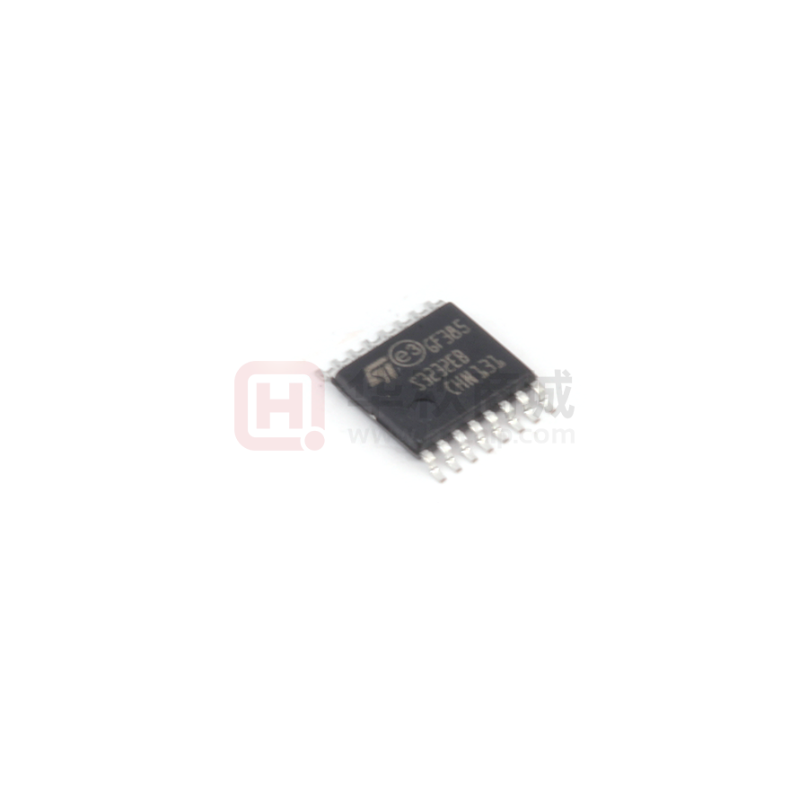
SO-16
TSSOP16
Features
• ESD protection for RS-232 I/O pins
The ST3232E has two receivers and two drivers.
• ±15 kV human body model
The device is guaranteed to run at data rates of
250 kbps while maintaining RS-232 output levels.
• ±8 kV IEC 1000-4-2 contact discharge
• 300 µA supply current
• 250 kbps minimum guaranteed data rate
• 6 V/µs minimum guaranteed slew rate
• Meet EIA/TIA-232 specifications down to 3 V
• Available in SO-16 and TSSOP16
Applications
• Notebook, subnotebook and palmtop
computers
• Battery-powered equipment
Table 1. Device summary
Order code
Temperature range
Package
ST3232ECDR
0 to 70 °C
SO-16 (tape and reel)
ST3232EBDR
-40 to 85 °C
SO-16 (tape and reel)
ST3232ECTR
0 to 70 °C
TSSOP16 (tape and reel)
ST3232EBTR
-40 to 85 °C
TSSOP16 (tape and reel)
July 2018
This is information on a product in full production.
DocID8784 Rev 7
1/14
www.st.com
�Contents
ST3232EB, ST3232EC
Contents
1
Pin configuration . . . . . . . . . . . . . . . . . . . . . . . . . . . . . . . . . . . . . . . . . . . . 3
2
Absolute maximum ratings . . . . . . . . . . . . . . . . . . . . . . . . . . . . . . . . . . . 4
3
Electrical characteristics . . . . . . . . . . . . . . . . . . . . . . . . . . . . . . . . . . . . . 5
4
Application . . . . . . . . . . . . . . . . . . . . . . . . . . . . . . . . . . . . . . . . . . . . . . . . . 7
5
Typical performance characteristics . . . . . . . . . . . . . . . . . . . . . . . . . . . . 8
6
Package information . . . . . . . . . . . . . . . . . . . . . . . . . . . . . . . . . . . . . . . . . 9
7
2/14
6.1
SO-16 package information . . . . . . . . . . . . . . . . . . . . . . . . . . . . . . . . . . . 10
6.2
TSSOP-16 package information . . . . . . . . . . . . . . . . . . . . . . . . . . . . . . . . 12
Revision history . . . . . . . . . . . . . . . . . . . . . . . . . . . . . . . . . . . . . . . . . . . 13
DocID8784 Rev 7
�ST3232EB, ST3232EC
1
Pin configuration
Pin configuration
Figure 1. Pin connection
Table 2. Pin description
Pin n°
Symbol
Name and function
1
C1+
Positive terminal for the first charge pump capacitor
2
V+
Doubled voltage terminal
3
C1-
Negative Terminal for the first charge pump capacitor
4
C2+
Positive terminal for the second charge pump capacitor
5
C2-
Negative terminal for the second charge pump capacitor
6
V-
Inverted voltage terminal
7
T2OUT
8
R2IN
9
R2OUT
Second receiver output voltage
10
T2IN
Second transmitter input voltage
11
T1IN
First transmitter input voltage
12
R1OUT
First receiver output voltage
13
R1IN
14
T1OUT
15
GND
Ground
16
VCC
Supply voltage
Second transmitter output voltage
Second receiver input voltage
First receiver input voltage
First transmitter output voltage
DocID8784 Rev 7
3/14
14
�Absolute maximum ratings
2
ST3232EB, ST3232EC
Absolute maximum ratings
Table 3. Absolute maximum ratings
Symbol
Parameter
Value
Unit
-0.3 to 6
V
VCC
Supply voltage
V+
Doubled voltage terminal
(VCC - 0.3) to 7
V
V-
Inverted voltage terminal
0.3 to -7
V
13
V
-0.3 to 6
V
± 25
V
± 13.2
V
-0.3 to (VCC + 0.3)
V
V+ +|V-|
TIN
Transmitter input voltage range
RIN
Receiver input voltage range
TOUT
Transmitter output voltage range
ROUT
Receiver output voltage range
tSHORT
Tj
Transmitter output short-to-ground time
Maximum junction temperature
Thermal resistance
Rth-jc
Continuous
150
SO-16
30
TSSOP16
25
Thermal resistance junction-to-ambient
Rth-ja
°C
junction-to-case(1) (2)
°C/W
(1) (2)
SO-16
95
TSSOP16
95
1. Short-circuits can cause excessive heating and destructive dissipation.
2. Rth are typical values.
Note:
Absolute maximum ratings are those values beyond which damage to the device may occur.
Functional operation under these condition is not implied.
Externally applied V+ and V- can have a maximum magnitude of +7 V, but their absolute
addition can not exceed 13 V.
Running on internal charge pump, intrinsic self limitation allows exceeding those values
without any damage.
Start-up voltage sequence (VCC, then V+, then V-) is critical, therefore it is not
recommended to use this device using externally applied voltage to V+ and V-.
Figure 2. ESD performance: transmitter outputs, receiver inputs
Symbol
4/14
Parameter
Test conditions
Min.
Typ.
Max.
Unit
ESD
ESD protection
voltage
Human body model
±15
kV
ESD
ESD protection
voltage
IEC-1000-4-2
±8
kV
DocID8784 Rev 7
�ST3232EB, ST3232EC
3
Electrical characteristics
Electrical characteristics
C1 - C4 = 0.1 µF, VCC = 3 V to 5.5 V, TA = -40 to 85 °C, unless otherwise specified. Typical
values are referred to TA = 25 °C.
Table 4. Electrical characteristics
Symbol
ISUPPLY
Parameter
Test conditions
Min.
VCC Power supply current No Load, VCC = 3 V or 5 V, TA = 25 °C
Typ.
Max.
Unit
0.3
1
mA
C1 - C4 = 0.1 µF, VCC = 3 V to 5.5 V, TA = -40 to 85 °C, unless otherwise specified. Typical
values are referred to TA = 25 °C.
Table 5. Logic input
Symbol
Parameter
VTIL
Input logic threshold low
VHYS
Transmitter input hysteresis
VTIH
Input logic threshold high
IIL
Test conditions
Typ.
T-IN
Max.
Unit
0.8
V
0.25
VCC = 3.3 V
VCC = 5 V
Input leakage current
Min.
V
2
V
2.4
± 0.01
T-IN
±1
µA
C1 - C4 = 0.1 µF tested at 3.3 V ± 10 %, VCC = 3 V to 5.5 V, TA = -40 to 85 °C, unless
otherwise specified. Typical values are referred to TA = 25 °C.
Table 6. Transmitter
Symbol
Parameter
Test conditions
Min.
Typ.
Max.
Unit
VTOUT
Output voltage swing
All transmitter outputs are loaded with
3 kΩ to GND
±5
± 5.4
V
RTOUT
Transmitter output
resistance
VCC = 0 V, VOUT = ± 2 V
300
10M
W
± 60
mA
ISC
Output short-circuit current
ITOL
Output leakage current
VCC = 0 V or 3.3 V to 5.5 V
VOUT = ± 12 V
Transmitters disable
DocID8784 Rev 7
± 25
µA
5/14
14
�Electrical characteristics
ST3232EB, ST3232EC
C1 - C4 = 0.1 µF tested at 3.3 V ± 10%, VCC = 3 V to 5.5 V, TA = -40 to 85 °C, unless
otherwise specified. Typical values are referred to TA = 25 °C.
Table 7. Receiver
Symbol
Parameter
Test conditions
VRIN
Receiver input voltage operating
range
VRIL
RS-232 input threshold low
VRIH
RS-232 input threshold high
Min.
Typ.
-25
TA = 25 °C, VCC = 3.3 V
0.6
1.1
TA = 25 °C, VCC = 5 V
0.8
1.5
Max.
Unit
25
V
V
TA = 25 °C, VCC = 3.3 V
1.4
2.4
TA = 25 °C, VCC = 5 V
1.8
2.4
VRIHYS
Input hysteresis
RRIN
Input resistance
TA = 25 °C
VROL
TTL/CMOS Output voltage low
IOUT = 1.6 mA
VROH
TTL/CMOS Output voltage high IOUT = -1 mA
V
0.5
3
VCC-0.6
V
5
7
kΩ
0.4
V
VCC-0.1
V
C1 - C4 = 0.1 µF tested at 3.3 V ± 10%, VCC = 3 V to 5.5 V, TA = -40 to 85 °C, unless
otherwise specified. Typical values are referred to TA = 25 °C
Table 8. Timing characteristics
Symbol
Parameter
Test conditions
Data transfer rate
RL = 3 kΩ, CL2= 1000 pF
one transmitter switching
tPHLR
tPLHR
Propagation delay input to
output
RXIN = RXOUT, CL = 150 pF
tOER
tODR
DR
Min.
Typ.
Max.
250
Unit
kbps
0.15
µs
Receiver output enable time Normal operation
50
ns
Receiver output disable time Normal operation
50
ns
|tPHLT
- tTHL|
Transmitter propagation
delay difference
200
ns
|tPHLR
- tTHR|
Receiver propagation delay
difference
50
ns
SRT
Transition slew rate
(1)
TA = 25 °C RL = 3 kΩ to 7 kΩ VCC=
3.3 V measured from +3 V to -3 V or -3 V
to +3 V
CL = 150 pF to 1000 pF
CL = 150 pF to 2500 pF
1. Transmitter skew is measured at the transmitter zero-cross points.
6/14
DocID8784 Rev 7
6
4
30
30
V/µs
V/µs
�ST3232EB, ST3232EC
4
Application
Application
Figure 3. Application circuits
Table 9. Capacitance value (µF)
VCC
C1
C2
C3
C4
Cbypass
3.0 to 3.6
0.1
0.1
0.1
0.1
0.1
4.5 to 5.5
0.047
0.33
0.33
0.33
0.1
3.0 to 5.5
0.1
0.47
0.47
0.47
0.1
DocID8784 Rev 7
7/14
14
�Typical performance characteristics
5
ST3232EB, ST3232EC
Typical performance characteristics
Unless otherwise specified TJ = 25 °C.
Figure 4. Output current vs. output high voltage Figure 5. Output current vs. output high voltage
Figure 6. Output current vs. output low voltage Figure 7. Output current vs. output low voltage
Figure 8. Voltage transfer characteristics for
transmitter inputs
8/14
Figure 9. Receiver input resistance
DocID8784 Rev 7
�ST3232EB, ST3232EC
6
Package information
Package information
In order to meet environmental requirements, ST offers these devices in different grades of
ECOPACK® packages, depending on their level of environmental compliance. ECOPACK®
specifications, grade definitions and product status are available at: www.st.com.
ECOPACK® is an ST trademark.
DocID8784 Rev 7
9/14
14
�Package information
6.1
ST3232EB, ST3232EC
SO-16 package information
Figure 10. SO-16 package outline
H
N
�
�
�
�
��
E
'
�������B*
Table 10. SO-16 package mechanical data
Dimensions (mm)
Ref.
Min.
Typ.
A
Max.
1.75
A1
0.10
A2
1.25
b
0.31
0.51
c
0.17
0.25
D
9.80
9.90
10.00
E
5.80
6.00
6.20
E1
3.80
3.90
4.00
e
0.25
1.27
h
0.25
0.50
L
0.40
1.27
k
0
8
ccc
0.10
Dimension D does not include mold flash, protrusions or gate burrs. Mold flash, protrusions
or gate burrs shall not exceed 0.15 mm in total (both side).
Dimension “E1” does not include interlead flash or protrusions.Interlead flash or protrusions
shall not exceed 0.25mm per side.
Dimensions referred to the bottom side of the package.
10/14
DocID8784 Rev 7
�ST3232EB, ST3232EC
Package information
Figure 11. SO-16 recommended footprint
DocID8784 Rev 7
11/14
14
�Package information
6.2
ST3232EB, ST3232EC
TSSOP-16 package information
Figure 12. TSSOP-16 package outline
�
�������B(
Table 11. TSSOP-16 package mechanical data
Dimensions
Ref.
mm
Min.
Typ.
A
Max.
1.20
A1
0.05
A2
0.80
b
0.19
0.30
c
0.09
0.20
D
4.90
5.00
5.10
E
6.20
6.40
6.60
E1
4.30
4.40
4.50
e
L
1.00
1.05
0.65
0.45
L1
k
0.15
0.60
0.75
1.00
0
aaa
8
0.10
TSSOP stands for thin shrink small outline package. Dimension “D” does not include mold
flash, protrusions or gate burrs. Mold flash, protrusions or gate burrs shall not exceed 0.15
mm per side. Dimension “E1” does not include interlead flash or protrusions. Interlead flash
or protrusions shall not exceed 0.25 mm per side.
12/14
DocID8784 Rev 7
�ST3232EB, ST3232EC
7
Revision history
Revision history
Table 12. Document revision history
Date
Revision
Changes
06-Sep-2006
3
Order codes updated.
21-Jan-2008
4
Added: Table 1 and note on Table 3.
08-Feb-2008
5
Modified: Table 1 on page 1.
05-Jan-2010
6
Modified: Table 1 on page 1.
04-Jul-2018
7
Updated Table 3: Absolute maximum ratings and Section 6: Package
information.
DocID8784 Rev 7
13/14
14
�ST3232EB, ST3232EC
IMPORTANT NOTICE – PLEASE READ CAREFULLY
STMicroelectronics NV and its subsidiaries (“ST”) reserve the right to make changes, corrections, enhancements, modifications, and
improvements to ST products and/or to this document at any time without notice. Purchasers should obtain the latest relevant information on
ST products before placing orders. ST products are sold pursuant to ST’s terms and conditions of sale in place at the time of order
acknowledgement.
Purchasers are solely responsible for the choice, selection, and use of ST products and ST assumes no liability for application assistance or
the design of Purchasers’ products.
No license, express or implied, to any intellectual property right is granted by ST herein.
Resale of ST products with provisions different from the information set forth herein shall void any warranty granted by ST for such product.
ST and the ST logo are trademarks of ST. All other product or service names are the property of their respective owners.
Information in this document supersedes and replaces information previously supplied in any prior versions of this document.
© 2018 STMicroelectronics – All rights reserved
14/14
DocID8784 Rev 7
�


 工商网监
湘ICP备2023018690号
工商网监
湘ICP备2023018690号
