ST92F124xx/ST92F150Cxx/
ST92F150JDV1/ST92F250CV2
8/16-bit single voltage Flash MCU family with RAM,
E³ TM (emulated EEPROM), CAN 2.0B and J1850 BLPD
Datasheet − production data
Features
■
Memories
– Internal memory: Single Voltage Flash up to 256
Kbytes, RAM up to 8 Kbytes, 1 Kbyte E3 TM
(Emulated EEPROM)
– In-Application Programming (IAP)
– 224 general purpose registers (register file)
available as RAM, accumulators or index
pointers
■
Clock, reset and supply management
– Register-oriented 8/16 bit CORE with RUN,
WFI, SLOW, HALT and STOP modes
– 0-24 MHz Operation (Int. Clock), 4.5-5.5 V
range
– PLL Clock Generator (3-5 MHz crystal)
– Minimum instruction time: 83 ns (24 MHz int.
clock)
■
Up to 80 I/O pins
■
Interrupt management
– 4 external fast interrupts + 1 NMI
– Up to 16 pins programmable as wake-up or
additional external interrupt with multi-level
interrupt handler
■
DMA controller for reduced processor overhead
■
Timers
– 16-bit Timer with 8-bit Prescaler, and Watchdog
Timer (activated by software or by hardware)
– 16-bit Standard Timer that can be used to
generate a time base independent of PLL Clock
Generator
– Two 16-bit independent Extended Function
Timers (EFTs) with Prescaler, up to two Input
Captures and up to two Output Compares
– Two 16-bit Multifunction Timers, with Prescaler,
up to two Input Captures and up to two Output
Compares
■
Communication interfaces
– Serial Peripheral Interface (SPI) with selectable
Master/Slave mode
July 2012
This is information on a product in full production.
LQFP64
PQFP100
14x14
14x20
LQFP100
14x14
– One Multiprotocol Serial Communications
Interface with asynchronous and synchronous
capabilities
– One asynchronous Serial Communications
Interface with 13-bit LIN Synch Break
generation capability
– J1850 Byte Level Protocol Decoder (JBLPD)
– Up to two full I²C multiple Master/Slave
Interfaces supporting Access Bus
– Up to two CAN 2.0B Active interfaces
■
Analog peripheral (low current coupling)
– 10-bit A/D Converter with up to 16 robust input
channels
■
Development tools
– Free High performance development
environment (IDE) based on Visual Debugger,
Assembler, Linker, and C-Compiler; Real Time
Operating System (OSEK OS, CMX) and CAN
drivers
– Hardware emulator and Flash programming
board for development and ISP Flasher for
production
Table 1.
Device summary
Reference
Part number
ST92F124xx
ST92F124R1, ST92F124R9,
ST92F124V1
ST92F150Cxx
ST92F150CR1, ST92F150CR9,
ST92F150CV1, ST92F150CV9
ST92F150JDxx
ST92F150JDV1
ST92F250Cxx
ST92F250CV2
Doc ID 8848 Rev 7
1/523
www.st.com
1
�Contents
ST92F124xx/ST92F150Cxx/ST92F150JDV1/ST92F250CV2
Contents
1
Description . . . . . . . . . . . . . . . . . . . . . . . . . . . . . . . . . . . . . . . . . . . . . . . . 20
2
Pinout and pin description . . . . . . . . . . . . . . . . . . . . . . . . . . . . . . . . . . . 27
2.1
I/O port alternate functions . . . . . . . . . . . . . . . . . . . . . . . . . . . . . . . . . . . . 28
2.2
Termination of unused pins . . . . . . . . . . . . . . . . . . . . . . . . . . . . . . . . . . . 28
3
Voltage regulator . . . . . . . . . . . . . . . . . . . . . . . . . . . . . . . . . . . . . . . . . . . 40
4
I/O ports . . . . . . . . . . . . . . . . . . . . . . . . . . . . . . . . . . . . . . . . . . . . . . . . . . 41
4.1
Alternate functions for I/O ports . . . . . . . . . . . . . . . . . . . . . . . . . . . . . . . . 43
5
Operating modes . . . . . . . . . . . . . . . . . . . . . . . . . . . . . . . . . . . . . . . . . . . 48
6
Device architecture . . . . . . . . . . . . . . . . . . . . . . . . . . . . . . . . . . . . . . . . . 49
6.1
Core architecture . . . . . . . . . . . . . . . . . . . . . . . . . . . . . . . . . . . . . . . . . . . 49
6.2
Memory spaces . . . . . . . . . . . . . . . . . . . . . . . . . . . . . . . . . . . . . . . . . . . . 49
6.3
Register file . . . . . . . . . . . . . . . . . . . . . . . . . . . . . . . . . . . . . . . . . . . . . . 49
6.2.2
Register addressing . . . . . . . . . . . . . . . . . . . . . . . . . . . . . . . . . . . . . . . . 51
System registers . . . . . . . . . . . . . . . . . . . . . . . . . . . . . . . . . . . . . . . . . . . . 53
6.3.1
Central interrupt control register . . . . . . . . . . . . . . . . . . . . . . . . . . . . . . 54
6.3.2
Flag register . . . . . . . . . . . . . . . . . . . . . . . . . . . . . . . . . . . . . . . . . . . . . . 55
6.3.3
Register pointing techniques . . . . . . . . . . . . . . . . . . . . . . . . . . . . . . . . . 57
6.3.4
Paged registers . . . . . . . . . . . . . . . . . . . . . . . . . . . . . . . . . . . . . . . . . . . 60
6.3.5
Mode register . . . . . . . . . . . . . . . . . . . . . . . . . . . . . . . . . . . . . . . . . . . . . 61
6.3.6
Stack pointers . . . . . . . . . . . . . . . . . . . . . . . . . . . . . . . . . . . . . . . . . . . . 62
6.4
Memory organization . . . . . . . . . . . . . . . . . . . . . . . . . . . . . . . . . . . . . . . . 65
6.5
Memory management unit . . . . . . . . . . . . . . . . . . . . . . . . . . . . . . . . . . . . 66
6.6
Address space extension . . . . . . . . . . . . . . . . . . . . . . . . . . . . . . . . . . . . . 66
6.7
2/523
6.2.1
6.6.1
Addressing 16-Kbyte pages . . . . . . . . . . . . . . . . . . . . . . . . . . . . . . . . . . 66
6.6.2
Addressing 64-Kbyte segments . . . . . . . . . . . . . . . . . . . . . . . . . . . . . . . 67
MMU registers . . . . . . . . . . . . . . . . . . . . . . . . . . . . . . . . . . . . . . . . . . . . . 68
6.7.1
DPR[3:0]: data page registers . . . . . . . . . . . . . . . . . . . . . . . . . . . . . . . . 68
6.7.2
CSR: Code segment register . . . . . . . . . . . . . . . . . . . . . . . . . . . . . . . . . 70
6.7.3
ISR: Interrupt segment register . . . . . . . . . . . . . . . . . . . . . . . . . . . . . . . 70
Doc ID 8848 Rev 7
�ST92F124xx/ST92F150Cxx/ST92F150JDV1/ST92F250CV2
6.7.4
6.8
7
MMU usage . . . . . . . . . . . . . . . . . . . . . . . . . . . . . . . . . . . . . . . . . . . . . . . 72
6.8.1
Normal program execution . . . . . . . . . . . . . . . . . . . . . . . . . . . . . . . . . . . 72
6.8.2
Interrupts . . . . . . . . . . . . . . . . . . . . . . . . . . . . . . . . . . . . . . . . . . . . . . . . 73
6.8.3
DMA . . . . . . . . . . . . . . . . . . . . . . . . . . . . . . . . . . . . . . . . . . . . . . . . . . . . 74
7.1
Introduction . . . . . . . . . . . . . . . . . . . . . . . . . . . . . . . . . . . . . . . . . . . . . . . 75
7.2
Functional description . . . . . . . . . . . . . . . . . . . . . . . . . . . . . . . . . . . . . . . 76
7.2.1
Structure . . . . . . . . . . . . . . . . . . . . . . . . . . . . . . . . . . . . . . . . . . . . . . . . 76
7.2.2
EEPROM emulation . . . . . . . . . . . . . . . . . . . . . . . . . . . . . . . . . . . . . . . . 76
7.2.3
Operation . . . . . . . . . . . . . . . . . . . . . . . . . . . . . . . . . . . . . . . . . . . . . . . . 78
7.2.4
E3 TM update operation . . . . . . . . . . . . . . . . . . . . . . . . . . . . . . . . . . . . 78
7.2.5
Important note on Flash erase suspend . . . . . . . . . . . . . . . . . . . . . . . . 79
Register description . . . . . . . . . . . . . . . . . . . . . . . . . . . . . . . . . . . . . . . . . 80
7.3.1
Control registers . . . . . . . . . . . . . . . . . . . . . . . . . . . . . . . . . . . . . . . . . . 80
7.3.2
Status registers . . . . . . . . . . . . . . . . . . . . . . . . . . . . . . . . . . . . . . . . . . . 84
7.4
Write operation example . . . . . . . . . . . . . . . . . . . . . . . . . . . . . . . . . . . . . 86
7.5
Protection strategy . . . . . . . . . . . . . . . . . . . . . . . . . . . . . . . . . . . . . . . . . . 87
7.6
7.5.1
Non volatile registers . . . . . . . . . . . . . . . . . . . . . . . . . . . . . . . . . . . . . . . 87
7.5.2
Temporary unprotection . . . . . . . . . . . . . . . . . . . . . . . . . . . . . . . . . . . . . 90
Flash in-system programming . . . . . . . . . . . . . . . . . . . . . . . . . . . . . . . . . 92
7.6.1
Code update routine . . . . . . . . . . . . . . . . . . . . . . . . . . . . . . . . . . . . . . . 92
Register and memory map . . . . . . . . . . . . . . . . . . . . . . . . . . . . . . . . . . . 95
8.1
Introduction . . . . . . . . . . . . . . . . . . . . . . . . . . . . . . . . . . . . . . . . . . . . . . . 95
8.2
Memory configuration . . . . . . . . . . . . . . . . . . . . . . . . . . . . . . . . . . . . . . . . 95
8.3
9
DMASR: DMA segment register . . . . . . . . . . . . . . . . . . . . . . . . . . . . . . 71
Single voltage Flash and E3™ (emulated EEPROM) . . . . . . . . . . . . . . 75
7.3
8
Contents
8.2.1
Reset vector location . . . . . . . . . . . . . . . . . . . . . . . . . . . . . . . . . . . . . . . 95
8.2.2
Location of vector for external watchdog refresh . . . . . . . . . . . . . . . . . . 95
ST92F124/F150/F250 register map . . . . . . . . . . . . . . . . . . . . . . . . . . . . 101
Interrupts . . . . . . . . . . . . . . . . . . . . . . . . . . . . . . . . . . . . . . . . . . . . . . . . 121
9.1
Introduction . . . . . . . . . . . . . . . . . . . . . . . . . . . . . . . . . . . . . . . . . . . . . . 121
9.1.1
9.2
On-chip peripheral interrupt sources . . . . . . . . . . . . . . . . . . . . . . . . . . 121
Interrupt vectoring . . . . . . . . . . . . . . . . . . . . . . . . . . . . . . . . . . . . . . . . . 122
9.2.1
Divide by zero trap . . . . . . . . . . . . . . . . . . . . . . . . . . . . . . . . . . . . . . . . 123
Doc ID 8848 Rev 7
3/523
�Contents
ST92F124xx/ST92F150Cxx/ST92F150JDV1/ST92F250CV2
9.2.2
9.3
Interrupt priority levels . . . . . . . . . . . . . . . . . . . . . . . . . . . . . . . . . . . . . . 124
9.4
Priority level arbitration . . . . . . . . . . . . . . . . . . . . . . . . . . . . . . . . . . . . . . 124
9.5
10
11
4/523
Segment paging during interrupt routines . . . . . . . . . . . . . . . . . . . . . . 123
9.4.1
Priority level 7 (Lowest) . . . . . . . . . . . . . . . . . . . . . . . . . . . . . . . . . . . . 124
9.4.2
Maximum depth of nesting . . . . . . . . . . . . . . . . . . . . . . . . . . . . . . . . . . 124
9.4.3
Simultaneous interrupts . . . . . . . . . . . . . . . . . . . . . . . . . . . . . . . . . . . . 125
9.4.4
Dynamic priority level modification . . . . . . . . . . . . . . . . . . . . . . . . . . . . 125
Arbitration modes . . . . . . . . . . . . . . . . . . . . . . . . . . . . . . . . . . . . . . . . . . 126
9.5.1
Concurrent mode . . . . . . . . . . . . . . . . . . . . . . . . . . . . . . . . . . . . . . . . . 126
9.5.2
Nested mode . . . . . . . . . . . . . . . . . . . . . . . . . . . . . . . . . . . . . . . . . . . . 129
9.6
External interrupts . . . . . . . . . . . . . . . . . . . . . . . . . . . . . . . . . . . . . . . . . 131
9.7
Standard interrupts (CAN and SCI-A) . . . . . . . . . . . . . . . . . . . . . . . . . . 135
9.7.1
Functional description . . . . . . . . . . . . . . . . . . . . . . . . . . . . . . . . . . . . . 135
9.7.2
Important note on standard interrupts . . . . . . . . . . . . . . . . . . . . . . . . . 137
9.8
Top level interrupt . . . . . . . . . . . . . . . . . . . . . . . . . . . . . . . . . . . . . . . . . . 137
9.9
Dedicated on-chip peripheral interrupts . . . . . . . . . . . . . . . . . . . . . . . . . 137
9.10
Interrupt response time . . . . . . . . . . . . . . . . . . . . . . . . . . . . . . . . . . . . . 138
9.11
Interrupt registers . . . . . . . . . . . . . . . . . . . . . . . . . . . . . . . . . . . . . . . . . . 139
9.12
Wake-up / interrupt lines management unit (WUIMU) . . . . . . . . . . . . . . 149
9.12.1
Introduction . . . . . . . . . . . . . . . . . . . . . . . . . . . . . . . . . . . . . . . . . . . . . 149
9.12.2
Main features . . . . . . . . . . . . . . . . . . . . . . . . . . . . . . . . . . . . . . . . . . . . 150
9.12.3
Functional description . . . . . . . . . . . . . . . . . . . . . . . . . . . . . . . . . . . . . 151
9.12.4
Programming considerations . . . . . . . . . . . . . . . . . . . . . . . . . . . . . . . . 154
9.12.5
Register description . . . . . . . . . . . . . . . . . . . . . . . . . . . . . . . . . . . . . . . 155
9.12.6
Important note on WUIMU . . . . . . . . . . . . . . . . . . . . . . . . . . . . . . . . . . 158
On-chip direct memory access (DMA) . . . . . . . . . . . . . . . . . . . . . . . . 159
10.1
Introduction . . . . . . . . . . . . . . . . . . . . . . . . . . . . . . . . . . . . . . . . . . . . . . 159
10.2
DMA priority levels . . . . . . . . . . . . . . . . . . . . . . . . . . . . . . . . . . . . . . . . . 159
10.3
DMA transactions . . . . . . . . . . . . . . . . . . . . . . . . . . . . . . . . . . . . . . . . . . 160
10.4
DMA cycle time . . . . . . . . . . . . . . . . . . . . . . . . . . . . . . . . . . . . . . . . . . . 162
10.5
Swap mode . . . . . . . . . . . . . . . . . . . . . . . . . . . . . . . . . . . . . . . . . . . . . . 162
10.6
DMA registers . . . . . . . . . . . . . . . . . . . . . . . . . . . . . . . . . . . . . . . . . . . . . 163
Reset and clock control unit (RCCU) . . . . . . . . . . . . . . . . . . . . . . . . . 165
Doc ID 8848 Rev 7
�ST92F124xx/ST92F150Cxx/ST92F150JDV1/ST92F250CV2
11.1
Introduction . . . . . . . . . . . . . . . . . . . . . . . . . . . . . . . . . . . . . . . . . . . . . . 165
11.2
Clock control unit . . . . . . . . . . . . . . . . . . . . . . . . . . . . . . . . . . . . . . . . . . 165
11.2.1
11.3
11.3.1
PLL clock multiplier programming . . . . . . . . . . . . . . . . . . . . . . . . . . . . 168
11.3.2
PLL free running mode . . . . . . . . . . . . . . . . . . . . . . . . . . . . . . . . . . . . 169
11.3.3
CPU clock prescaling . . . . . . . . . . . . . . . . . . . . . . . . . . . . . . . . . . . . . . 169
11.3.4
Peripheral clock . . . . . . . . . . . . . . . . . . . . . . . . . . . . . . . . . . . . . . . . . . 170
11.3.5
Low power modes . . . . . . . . . . . . . . . . . . . . . . . . . . . . . . . . . . . . . . . . 170
11.3.6
Interrupt generation . . . . . . . . . . . . . . . . . . . . . . . . . . . . . . . . . . . . . . . 171
11.4
Clock control registers . . . . . . . . . . . . . . . . . . . . . . . . . . . . . . . . . . . . . . 174
11.5
Crystal oscillator . . . . . . . . . . . . . . . . . . . . . . . . . . . . . . . . . . . . . . . . . . . 180
11.6
Reset/stop manager . . . . . . . . . . . . . . . . . . . . . . . . . . . . . . . . . . . . . . . . 183
Reset pin timing . . . . . . . . . . . . . . . . . . . . . . . . . . . . . . . . . . . . . . . . . . 184
External memory interface (EXTMI) . . . . . . . . . . . . . . . . . . . . . . . . . . . 186
12.1
Introduction . . . . . . . . . . . . . . . . . . . . . . . . . . . . . . . . . . . . . . . . . . . . . . 186
12.2
External memory signals . . . . . . . . . . . . . . . . . . . . . . . . . . . . . . . . . . . . 186
12.3
13
Clock control unit overview . . . . . . . . . . . . . . . . . . . . . . . . . . . . . . . . . 165
Clock management . . . . . . . . . . . . . . . . . . . . . . . . . . . . . . . . . . . . . . . . 167
11.6.1
12
Contents
12.2.1
AS: Address strobe . . . . . . . . . . . . . . . . . . . . . . . . . . . . . . . . . . . . . . . 187
12.2.2
DS: Data strobe . . . . . . . . . . . . . . . . . . . . . . . . . . . . . . . . . . . . . . . . . . 187
12.2.3
RW: Read/write . . . . . . . . . . . . . . . . . . . . . . . . . . . . . . . . . . . . . . . . . . 187
12.2.4
DS2: Data strobe 2 . . . . . . . . . . . . . . . . . . . . . . . . . . . . . . . . . . . . . . . 187
12.2.5
PORT 0 . . . . . . . . . . . . . . . . . . . . . . . . . . . . . . . . . . . . . . . . . . . . . . . . 188
12.2.6
PORT 1 . . . . . . . . . . . . . . . . . . . . . . . . . . . . . . . . . . . . . . . . . . . . . . . . 188
12.2.7
PORT 9 [7:2] . . . . . . . . . . . . . . . . . . . . . . . . . . . . . . . . . . . . . . . . . . . . 188
12.2.8
WAIT: External memory wait . . . . . . . . . . . . . . . . . . . . . . . . . . . . . . . . 190
Register description . . . . . . . . . . . . . . . . . . . . . . . . . . . . . . . . . . . . . . . . 191
I/O ports . . . . . . . . . . . . . . . . . . . . . . . . . . . . . . . . . . . . . . . . . . . . . . . . . 195
13.1
Introduction . . . . . . . . . . . . . . . . . . . . . . . . . . . . . . . . . . . . . . . . . . . . . . 195
13.2
Specific port configurations . . . . . . . . . . . . . . . . . . . . . . . . . . . . . . . . . . 195
13.3
Port control registers . . . . . . . . . . . . . . . . . . . . . . . . . . . . . . . . . . . . . . . 195
13.4
Input/output bit configuration . . . . . . . . . . . . . . . . . . . . . . . . . . . . . . . . . 196
13.5
Alternate function architecture . . . . . . . . . . . . . . . . . . . . . . . . . . . . . . . . 200
13.5.1
Pin declared as I/O . . . . . . . . . . . . . . . . . . . . . . . . . . . . . . . . . . . . . . . 200
13.5.2
Pin declared as an alternate function input . . . . . . . . . . . . . . . . . . . . . 200
Doc ID 8848 Rev 7
5/523
�Contents
ST92F124xx/ST92F150Cxx/ST92F150JDV1/ST92F250CV2
13.5.3
13.6
14
I/O status after Wfi, Halt and Reset . . . . . . . . . . . . . . . . . . . . . . . . . . . . 201
On-chip peripherals . . . . . . . . . . . . . . . . . . . . . . . . . . . . . . . . . . . . . . . 203
14.1
14.2
14.3
14.4
14.5
6/523
Pin declared as an alternate function output . . . . . . . . . . . . . . . . . . . . 201
Timer/watchdog (WDT) . . . . . . . . . . . . . . . . . . . . . . . . . . . . . . . . . . . . . 203
14.1.1
Introduction . . . . . . . . . . . . . . . . . . . . . . . . . . . . . . . . . . . . . . . . . . . . . 203
14.1.2
Functional description . . . . . . . . . . . . . . . . . . . . . . . . . . . . . . . . . . . . . 204
14.1.3
Watchdog timer operation . . . . . . . . . . . . . . . . . . . . . . . . . . . . . . . . . . 206
14.1.4
WDT interrupts . . . . . . . . . . . . . . . . . . . . . . . . . . . . . . . . . . . . . . . . . . . 208
14.1.5
Register description . . . . . . . . . . . . . . . . . . . . . . . . . . . . . . . . . . . . . . . 209
Standard timer (STIM) . . . . . . . . . . . . . . . . . . . . . . . . . . . . . . . . . . . . . . 213
14.2.1
Introduction . . . . . . . . . . . . . . . . . . . . . . . . . . . . . . . . . . . . . . . . . . . . . 213
14.2.2
Functional description . . . . . . . . . . . . . . . . . . . . . . . . . . . . . . . . . . . . . 214
14.2.3
Interrupt selection . . . . . . . . . . . . . . . . . . . . . . . . . . . . . . . . . . . . . . . . 215
14.2.4
Register description . . . . . . . . . . . . . . . . . . . . . . . . . . . . . . . . . . . . . . . 216
Extended function timer (EFT) . . . . . . . . . . . . . . . . . . . . . . . . . . . . . . . . 217
14.3.1
Introduction . . . . . . . . . . . . . . . . . . . . . . . . . . . . . . . . . . . . . . . . . . . . . 217
14.3.2
Main features . . . . . . . . . . . . . . . . . . . . . . . . . . . . . . . . . . . . . . . . . . . . 218
14.3.3
Functional description . . . . . . . . . . . . . . . . . . . . . . . . . . . . . . . . . . . . . 218
14.3.4
Interrupt management . . . . . . . . . . . . . . . . . . . . . . . . . . . . . . . . . . . . . 231
14.3.5
Register description . . . . . . . . . . . . . . . . . . . . . . . . . . . . . . . . . . . . . . . 233
Multifunction timer (MFT) . . . . . . . . . . . . . . . . . . . . . . . . . . . . . . . . . . . . 241
14.4.1
Introduction . . . . . . . . . . . . . . . . . . . . . . . . . . . . . . . . . . . . . . . . . . . . . 241
14.4.2
Functional description . . . . . . . . . . . . . . . . . . . . . . . . . . . . . . . . . . . . . 243
14.4.3
Input pin assignment . . . . . . . . . . . . . . . . . . . . . . . . . . . . . . . . . . . . . . 247
14.4.4
Output pin assignment . . . . . . . . . . . . . . . . . . . . . . . . . . . . . . . . . . . . . 252
14.4.5
Interrupt and DMA . . . . . . . . . . . . . . . . . . . . . . . . . . . . . . . . . . . . . . . . 254
14.4.6
Register description . . . . . . . . . . . . . . . . . . . . . . . . . . . . . . . . . . . . . . . 258
Multiprotocol serial communications interface (SCI-M) . . . . . . . . . . . . . 273
14.5.1
Introduction . . . . . . . . . . . . . . . . . . . . . . . . . . . . . . . . . . . . . . . . . . . . . 273
14.5.2
Main features . . . . . . . . . . . . . . . . . . . . . . . . . . . . . . . . . . . . . . . . . . . . 273
14.5.3
Functional description . . . . . . . . . . . . . . . . . . . . . . . . . . . . . . . . . . . . . 274
14.5.4
SCI-M operating modes . . . . . . . . . . . . . . . . . . . . . . . . . . . . . . . . . . . . 275
14.5.5
Serial frame format . . . . . . . . . . . . . . . . . . . . . . . . . . . . . . . . . . . . . . . 277
14.5.6
Clocks and serial transmission rates . . . . . . . . . . . . . . . . . . . . . . . . . . 280
14.5.7
SCI -M initialization procedure . . . . . . . . . . . . . . . . . . . . . . . . . . . . . . . 281
Doc ID 8848 Rev 7
�ST92F124xx/ST92F150Cxx/ST92F150JDV1/ST92F250CV2
Contents
14.5.8
Input signals . . . . . . . . . . . . . . . . . . . . . . . . . . . . . . . . . . . . . . . . . . . . . 283
14.5.9
Output signals . . . . . . . . . . . . . . . . . . . . . . . . . . . . . . . . . . . . . . . . . . . 283
14.5.10 Interrupts and DMA . . . . . . . . . . . . . . . . . . . . . . . . . . . . . . . . . . . . . . . 284
14.5.11 Register description . . . . . . . . . . . . . . . . . . . . . . . . . . . . . . . . . . . . . . . 287
14.6
14.7
14.8
14.9
Asynchronous serial communications interface (SCI-A) . . . . . . . . . . . . 300
14.6.1
Introduction . . . . . . . . . . . . . . . . . . . . . . . . . . . . . . . . . . . . . . . . . . . . . 300
14.6.2
Main features . . . . . . . . . . . . . . . . . . . . . . . . . . . . . . . . . . . . . . . . . . . . 301
14.6.3
General description . . . . . . . . . . . . . . . . . . . . . . . . . . . . . . . . . . . . . . . 301
14.6.4
Functional description . . . . . . . . . . . . . . . . . . . . . . . . . . . . . . . . . . . . . 303
14.6.5
Register description . . . . . . . . . . . . . . . . . . . . . . . . . . . . . . . . . . . . . . . 309
14.6.6
Important notes on SCI-A . . . . . . . . . . . . . . . . . . . . . . . . . . . . . . . . . . 317
Serial peripheral interface (SPI) . . . . . . . . . . . . . . . . . . . . . . . . . . . . . . . 317
14.7.1
Introduction . . . . . . . . . . . . . . . . . . . . . . . . . . . . . . . . . . . . . . . . . . . . . 317
14.7.2
Main features . . . . . . . . . . . . . . . . . . . . . . . . . . . . . . . . . . . . . . . . . . . . 317
14.7.3
General description . . . . . . . . . . . . . . . . . . . . . . . . . . . . . . . . . . . . . . . 317
14.7.4
Functional description . . . . . . . . . . . . . . . . . . . . . . . . . . . . . . . . . . . . . 319
14.7.5
Interrupt management . . . . . . . . . . . . . . . . . . . . . . . . . . . . . . . . . . . . . 326
14.7.6
Register description . . . . . . . . . . . . . . . . . . . . . . . . . . . . . . . . . . . . . . . 327
I2C bus interface . . . . . . . . . . . . . . . . . . . . . . . . . . . . . . . . . . . . . . . . . . 331
14.8.1
Introduction . . . . . . . . . . . . . . . . . . . . . . . . . . . . . . . . . . . . . . . . . . . . . 331
14.8.2
Main features . . . . . . . . . . . . . . . . . . . . . . . . . . . . . . . . . . . . . . . . . . . . 331
14.8.3
Functional description . . . . . . . . . . . . . . . . . . . . . . . . . . . . . . . . . . . . . 333
14.8.4
I2C state machine . . . . . . . . . . . . . . . . . . . . . . . . . . . . . . . . . . . . . . . . 335
14.8.5
Interrupt features . . . . . . . . . . . . . . . . . . . . . . . . . . . . . . . . . . . . . . . . . 340
14.8.6
DMA features . . . . . . . . . . . . . . . . . . . . . . . . . . . . . . . . . . . . . . . . . . . . 342
14.8.7
Register description . . . . . . . . . . . . . . . . . . . . . . . . . . . . . . . . . . . . . . . 344
14.8.8
Important notes on I2C . . . . . . . . . . . . . . . . . . . . . . . . . . . . . . . . . . . . 359
J1850 byte level protocol decoder (JBLPD) . . . . . . . . . . . . . . . . . . . . . . 359
14.9.1
Introduction . . . . . . . . . . . . . . . . . . . . . . . . . . . . . . . . . . . . . . . . . . . . . 359
14.9.2
Main features . . . . . . . . . . . . . . . . . . . . . . . . . . . . . . . . . . . . . . . . . . . . 360
14.9.3
Functional description . . . . . . . . . . . . . . . . . . . . . . . . . . . . . . . . . . . . . 361
14.9.4
Peripheral functional modes . . . . . . . . . . . . . . . . . . . . . . . . . . . . . . . . 373
14.9.5
Interrupt features . . . . . . . . . . . . . . . . . . . . . . . . . . . . . . . . . . . . . . . . . 374
14.9.6
DMA features . . . . . . . . . . . . . . . . . . . . . . . . . . . . . . . . . . . . . . . . . . . . 376
14.9.7
Register description . . . . . . . . . . . . . . . . . . . . . . . . . . . . . . . . . . . . . . . 380
14.10 Controller area network (bxCAN) . . . . . . . . . . . . . . . . . . . . . . . . . . . . . . 406
Doc ID 8848 Rev 7
7/523
�Contents
ST92F124xx/ST92F150Cxx/ST92F150JDV1/ST92F250CV2
14.10.1 Introduction . . . . . . . . . . . . . . . . . . . . . . . . . . . . . . . . . . . . . . . . . . . . . 406
14.10.2 Main features . . . . . . . . . . . . . . . . . . . . . . . . . . . . . . . . . . . . . . . . . . . . 406
14.10.3 General description . . . . . . . . . . . . . . . . . . . . . . . . . . . . . . . . . . . . . . . 407
14.10.4 Operating modes . . . . . . . . . . . . . . . . . . . . . . . . . . . . . . . . . . . . . . . . . 409
14.10.5 Functional description . . . . . . . . . . . . . . . . . . . . . . . . . . . . . . . . . . . . . 412
14.10.6 Interrupts . . . . . . . . . . . . . . . . . . . . . . . . . . . . . . . . . . . . . . . . . . . . . . . 424
14.10.7 Register access protection . . . . . . . . . . . . . . . . . . . . . . . . . . . . . . . . . 426
14.10.8 Register description . . . . . . . . . . . . . . . . . . . . . . . . . . . . . . . . . . . . . . . 426
14.10.9 Important notes on CAN . . . . . . . . . . . . . . . . . . . . . . . . . . . . . . . . . . . 451
14.11 10-bit analog to digital converter (ADC) . . . . . . . . . . . . . . . . . . . . . . . . . 451
14.11.1 Main characteristics . . . . . . . . . . . . . . . . . . . . . . . . . . . . . . . . . . . . . . . 451
14.11.2 Introduction . . . . . . . . . . . . . . . . . . . . . . . . . . . . . . . . . . . . . . . . . . . . . 451
14.11.3 Functional description . . . . . . . . . . . . . . . . . . . . . . . . . . . . . . . . . . . . . 453
14.11.4 Interrupts . . . . . . . . . . . . . . . . . . . . . . . . . . . . . . . . . . . . . . . . . . . . . . . 455
14.11.5 Register description . . . . . . . . . . . . . . . . . . . . . . . . . . . . . . . . . . . . . . . 456
15
Electrical characteristics . . . . . . . . . . . . . . . . . . . . . . . . . . . . . . . . . . . 471
15.1
DC electrical characteristics . . . . . . . . . . . . . . . . . . . . . . . . . . . . . . . . . . 472
15.2
AC electrical characteristics . . . . . . . . . . . . . . . . . . . . . . . . . . . . . . . . . . 474
15.3
Flash / E3 TM specifications . . . . . . . . . . . . . . . . . . . . . . . . . . . . . . . . . 476
15.4
EMC characteristics . . . . . . . . . . . . . . . . . . . . . . . . . . . . . . . . . . . . . . . . 477
15.5
RCCU characteristics . . . . . . . . . . . . . . . . . . . . . . . . . . . . . . . . . . . . . . . 481
15.6
PLL characteristics . . . . . . . . . . . . . . . . . . . . . . . . . . . . . . . . . . . . . . . . . 482
15.7
Oscillator characteristics . . . . . . . . . . . . . . . . . . . . . . . . . . . . . . . . . . . . 482
15.8
External bus timing . . . . . . . . . . . . . . . . . . . . . . . . . . . . . . . . . . . . . . . . . 483
15.9
Watchdog timing . . . . . . . . . . . . . . . . . . . . . . . . . . . . . . . . . . . . . . . . . . . 484
15.10 Standard timer timing . . . . . . . . . . . . . . . . . . . . . . . . . . . . . . . . . . . . . . . 485
15.11 Extended function timer external timing . . . . . . . . . . . . . . . . . . . . . . . . . 486
15.12 Multifunction timer external timing . . . . . . . . . . . . . . . . . . . . . . . . . . . . . 487
15.13 SCI timing . . . . . . . . . . . . . . . . . . . . . . . . . . . . . . . . . . . . . . . . . . . . . . . . 488
15.14 SPI timing . . . . . . . . . . . . . . . . . . . . . . . . . . . . . . . . . . . . . . . . . . . . . . . . 489
15.15 I2C/DDC-bus timing . . . . . . . . . . . . . . . . . . . . . . . . . . . . . . . . . . . . . . . . 491
15.16 J1850 byte level protocol decoder timing . . . . . . . . . . . . . . . . . . . . . . . . 493
15.17 10-bit ADC characteristics . . . . . . . . . . . . . . . . . . . . . . . . . . . . . . . . . . . 494
8/523
Doc ID 8848 Rev 7
�ST92F124xx/ST92F150Cxx/ST92F150JDV1/ST92F250CV2
16
General information . . . . . . . . . . . . . . . . . . . . . . . . . . . . . . . . . . . . . . . 497
16.1
Ordering information . . . . . . . . . . . . . . . . . . . . . . . . . . . . . . . . . . . . . . . 497
16.2
Version-specific sales conditions . . . . . . . . . . . . . . . . . . . . . . . . . . . . . . 497
16.3
Package mechanical data . . . . . . . . . . . . . . . . . . . . . . . . . . . . . . . . . . . 499
16.4
Soldering and glueability information . . . . . . . . . . . . . . . . . . . . . . . . . . . 500
16.5
Development tools . . . . . . . . . . . . . . . . . . . . . . . . . . . . . . . . . . . . . . . . . 500
16.5.1
17
Contents
Socket and emulator adapter information . . . . . . . . . . . . . . . . . . . . . . 501
Known limitations . . . . . . . . . . . . . . . . . . . . . . . . . . . . . . . . . . . . . . . . . 502
17.1
FLASH erase suspend limitations . . . . . . . . . . . . . . . . . . . . . . . . . . . . . 502
17.1.1
Description . . . . . . . . . . . . . . . . . . . . . . . . . . . . . . . . . . . . . . . . . . . . . . 502
17.1.2
Workaround . . . . . . . . . . . . . . . . . . . . . . . . . . . . . . . . . . . . . . . . . . . . . 503
17.2
Flash corruption when exiting stop mode . . . . . . . . . . . . . . . . . . . . . . . . 503
17.3
I2C limitations . . . . . . . . . . . . . . . . . . . . . . . . . . . . . . . . . . . . . . . . . . . . . 504
17.3.1
Start condition ignored in multimaster mode . . . . . . . . . . . . . . . . . . . . 505
17.3.2
Missing BUS error in master transmitter mode . . . . . . . . . . . . . . . . . . 505
17.3.3
AF bit (acknowledge failure flag) in transmitter mode
(slave and master) . . . . . . . . . . . . . . . . . . . . . . . . . . . . . . . . . . . . . . . . 505
17.3.4
BUSY flag in multimaster mode . . . . . . . . . . . . . . . . . . . . . . . . . . . . . . 506
17.3.5
ARLO (arbitration lost) flag in multimaster mode . . . . . . . . . . . . . . . . . 506
17.3.6
BUSY flag gets cleared when BUS error occurs . . . . . . . . . . . . . . . . . 506
17.4
SCI-A and CAN interrupts . . . . . . . . . . . . . . . . . . . . . . . . . . . . . . . . . . . 506
17.5
SCI-A mute mode . . . . . . . . . . . . . . . . . . . . . . . . . . . . . . . . . . . . . . . . . . 507
17.5.1
Mute mode description . . . . . . . . . . . . . . . . . . . . . . . . . . . . . . . . . . . . 507
17.5.2
Limitation description . . . . . . . . . . . . . . . . . . . . . . . . . . . . . . . . . . . . . . 507
17.5.3
Workaround . . . . . . . . . . . . . . . . . . . . . . . . . . . . . . . . . . . . . . . . . . . . . 508
17.6
CAN FIFO corruption when 2 FIFO messages are pending . . . . . . . . . 508
17.7
MFT DMA mask bit reset when MFT0 DMA priority level is set to 0 . . . 513
17.8
Emulation chip limitations . . . . . . . . . . . . . . . . . . . . . . . . . . . . . . . . . . . . 516
17.8.1
Reset behavior for bi-directional, weak pull-up ports . . . . . . . . . . . . . . 516
17.8.2
High drive I/Os when BSZ=1 . . . . . . . . . . . . . . . . . . . . . . . . . . . . . . . . 517
17.8.3
ADC parasitic diode . . . . . . . . . . . . . . . . . . . . . . . . . . . . . . . . . . . . . . . 517
17.8.4
ADC accuracy vs. negative injection current . . . . . . . . . . . . . . . . . . . . 518
17.8.5
I2CECCR register limitation . . . . . . . . . . . . . . . . . . . . . . . . . . . . . . . . . 519
17.8.6
I2C behavior disturbed during DMA transactions . . . . . . . . . . . . . . . . 519
17.8.7
MFT DMA mask bit reset . . . . . . . . . . . . . . . . . . . . . . . . . . . . . . . . . . . 519
Doc ID 8848 Rev 7
9/523
�Contents
ST92F124xx/ST92F150Cxx/ST92F150JDV1/ST92F250CV2
17.8.8
DMA data corrupted by MFT input capture . . . . . . . . . . . . . . . . . . . . . 519
17.8.9
SCI-A wrong break duration . . . . . . . . . . . . . . . . . . . . . . . . . . . . . . . . 520
17.8.10 LIN master mode not available on SCI-A . . . . . . . . . . . . . . . . . . . . . . . 521
17.8.11 Limitations on LQFP64 devices . . . . . . . . . . . . . . . . . . . . . . . . . . . . . . 521
18
10/523
Revision history . . . . . . . . . . . . . . . . . . . . . . . . . . . . . . . . . . . . . . . . . . 522
Doc ID 8848 Rev 7
�ST92F124xx/ST92F150Cxx/ST92F150JDV1/ST92F250CV2
List of tables
List of tables
Table 1.
Table 2.
Table 3.
Table 4.
Table 5.
Table 6.
Table 7.
Table 8.
Table 9.
Table 10.
Table 11.
Table 12.
Table 13.
Table 14.
Table 15.
Table 16.
Table 17.
Table 18.
Table 19.
Table 20.
Table 21.
Table 22.
Table 23.
Table 24.
Table 25.
Table 26.
Table 27.
Table 28.
Table 29.
Table 30.
Table 31.
Table 32.
Table 33.
Table 34.
Table 35.
Table 36.
Table 37.
Table 38.
Table 39.
Table 40.
Table 41.
Table 42.
Table 43.
Table 44.
Table 45.
Table 46.
Table 47.
Table 48.
Device summary . . . . . . . . . . . . . . . . . . . . . . . . . . . . . . . . . . . . . . . . . . . . . . . . . . . . . . . . . . 1
Detailed device summary . . . . . . . . . . . . . . . . . . . . . . . . . . . . . . . . . . . . . . . . . . . . . . . . . 19
ST92F124/F150/F250 power supply pins . . . . . . . . . . . . . . . . . . . . . . . . . . . . . . . . . . . . . . 38
ST92F124/F150/F250 primary function pins . . . . . . . . . . . . . . . . . . . . . . . . . . . . . . . . . . . 39
I/O port characteristics . . . . . . . . . . . . . . . . . . . . . . . . . . . . . . . . . . . . . . . . . . . . . . . . . . . . 41
I/O port alternate functions . . . . . . . . . . . . . . . . . . . . . . . . . . . . . . . . . . . . . . . . . . . . . . . . . 43
Register file organization . . . . . . . . . . . . . . . . . . . . . . . . . . . . . . . . . . . . . . . . . . . . . . . . . . 52
System registers (group E) . . . . . . . . . . . . . . . . . . . . . . . . . . . . . . . . . . . . . . . . . . . . . . . . . 53
Memory structure for 64K Flash device . . . . . . . . . . . . . . . . . . . . . . . . . . . . . . . . . . . . . . . 77
Memory structure for 128K Flash device . . . . . . . . . . . . . . . . . . . . . . . . . . . . . . . . . . . . . . 77
Memory structure for 256K Flash device . . . . . . . . . . . . . . . . . . . . . . . . . . . . . . . . . . . . . . 77
Sector status bits . . . . . . . . . . . . . . . . . . . . . . . . . . . . . . . . . . . . . . . . . . . . . . . . . . . . . . . . 84
Flash write operations. . . . . . . . . . . . . . . . . . . . . . . . . . . . . . . . . . . . . . . . . . . . . . . . . . . . . 86
E3 TM Write operations . . . . . . . . . . . . . . . . . . . . . . . . . . . . . . . . . . . . . . . . . . . . . . . . . . . 86
SCI0 registers (page 24) initialization . . . . . . . . . . . . . . . . . . . . . . . . . . . . . . . . . . . . . . . . . 93
User routine parameters . . . . . . . . . . . . . . . . . . . . . . . . . . . . . . . . . . . . . . . . . . . . . . . . . . . 95
Common registers . . . . . . . . . . . . . . . . . . . . . . . . . . . . . . . . . . . . . . . . . . . . . . . . . . . . . . 101
Group F pages register map (0 to 40) . . . . . . . . . . . . . . . . . . . . . . . . . . . . . . . . . . . . . . . 102
Group F pages register map (41 to 63) . . . . . . . . . . . . . . . . . . . . . . . . . . . . . . . . . . . . . . 103
Detailed register map . . . . . . . . . . . . . . . . . . . . . . . . . . . . . . . . . . . . . . . . . . . . . . . . . . . . 104
ENCSR . . . . . . . . . . . . . . . . . . . . . . . . . . . . . . . . . . . . . . . . . . . . . . . . . . . . . . . . . . . . . . . 124
Daisy chain priority . . . . . . . . . . . . . . . . . . . . . . . . . . . . . . . . . . . . . . . . . . . . . . . . . . . . . . 125
External interrupt channel grouping . . . . . . . . . . . . . . . . . . . . . . . . . . . . . . . . . . . . . . . . . 131
Multiplexed interrupt sources . . . . . . . . . . . . . . . . . . . . . . . . . . . . . . . . . . . . . . . . . . . . . . 133
Interrupt channel assignment . . . . . . . . . . . . . . . . . . . . . . . . . . . . . . . . . . . . . . . . . . . . . . 135
EIPLR . . . . . . . . . . . . . . . . . . . . . . . . . . . . . . . . . . . . . . . . . . . . . . . . . . . . . . . . . . . . . . . . 142
SIVR . . . . . . . . . . . . . . . . . . . . . . . . . . . . . . . . . . . . . . . . . . . . . . . . . . . . . . . . . . . . . . . . . 146
PL bit assignment . . . . . . . . . . . . . . . . . . . . . . . . . . . . . . . . . . . . . . . . . . . . . . . . . . . . . . . 147
PL bit meaning . . . . . . . . . . . . . . . . . . . . . . . . . . . . . . . . . . . . . . . . . . . . . . . . . . . . . . . . . 147
Channel E to H priority levels . . . . . . . . . . . . . . . . . . . . . . . . . . . . . . . . . . . . . . . . . . . . . . 148
Standard interrupt channel register map (Page 60) . . . . . . . . . . . . . . . . . . . . . . . . . . . . . 149
DM and IM meanings . . . . . . . . . . . . . . . . . . . . . . . . . . . . . . . . . . . . . . . . . . . . . . . . . . . . 164
Source priority levels . . . . . . . . . . . . . . . . . . . . . . . . . . . . . . . . . . . . . . . . . . . . . . . . . . . . 164
Free running clock frequency . . . . . . . . . . . . . . . . . . . . . . . . . . . . . . . . . . . . . . . . . . . . . . 169
Summary of operating modes using main crystal controlled oscillator . . . . . . . . . . . . . . . 172
Reset flags . . . . . . . . . . . . . . . . . . . . . . . . . . . . . . . . . . . . . . . . . . . . . . . . . . . . . . . . . . . . 177
PLL multiplication factors . . . . . . . . . . . . . . . . . . . . . . . . . . . . . . . . . . . . . . . . . . . . . . . . . 179
PLL divider factors . . . . . . . . . . . . . . . . . . . . . . . . . . . . . . . . . . . . . . . . . . . . . . . . . . . . . . 179
Maximum RS values . . . . . . . . . . . . . . . . . . . . . . . . . . . . . . . . . . . . . . . . . . . . . . . . . . . . . 181
Obtained results . . . . . . . . . . . . . . . . . . . . . . . . . . . . . . . . . . . . . . . . . . . . . . . . . . . . . . . . 182
I/O register map . . . . . . . . . . . . . . . . . . . . . . . . . . . . . . . . . . . . . . . . . . . . . . . . . . . . . . . . 196
Control bits . . . . . . . . . . . . . . . . . . . . . . . . . . . . . . . . . . . . . . . . . . . . . . . . . . . . . . . . . . . . 197
Port bit configuration table (n = 0, 1... 7; X = port number). . . . . . . . . . . . . . . . . . . . . . . . 197
Status of the I/O ports . . . . . . . . . . . . . . . . . . . . . . . . . . . . . . . . . . . . . . . . . . . . . . . . . . . . 202
Interrupt configuration . . . . . . . . . . . . . . . . . . . . . . . . . . . . . . . . . . . . . . . . . . . . . . . . . . . . 209
Input mode selection. . . . . . . . . . . . . . . . . . . . . . . . . . . . . . . . . . . . . . . . . . . . . . . . . . . . . 211
Clock input . . . . . . . . . . . . . . . . . . . . . . . . . . . . . . . . . . . . . . . . . . . . . . . . . . . . . . . . . . . . 217
Output modes . . . . . . . . . . . . . . . . . . . . . . . . . . . . . . . . . . . . . . . . . . . . . . . . . . . . . . . . . . 217
Doc ID 8848 Rev 7
11/523
�List of tables
Table 49.
Table 50.
Table 51.
Table 52.
Table 53.
Table 54.
Table 55.
Table 56.
Table 57.
Table 58.
Table 59.
Table 60.
Table 61.
Table 62.
Table 63.
Table 64.
Table 65.
Table 66.
Table 67.
Table 68.
Table 69.
Table 70.
Table 71.
Table 72.
Table 73.
Table 74.
Table 75.
Table 76.
Table 77.
Table 78.
Table 79.
Table 80.
Table 81.
Table 82.
Table 83.
Table 84.
Table 85.
Table 86.
Table 87.
Table 88.
Table 89.
Table 90.
Table 91.
Table 92.
Table 93.
Table 94.
Table 95.
Table 96.
Table 97.
Table 98.
Table 99.
Table 100.
12/523
ST92F124xx/ST92F150Cxx/ST92F150JDV1/ST92F250CV2
EFT pin naming conventions . . . . . . . . . . . . . . . . . . . . . . . . . . . . . . . . . . . . . . . . . . . . . . 218
Clock control bits . . . . . . . . . . . . . . . . . . . . . . . . . . . . . . . . . . . . . . . . . . . . . . . . . . . . . . . 238
Extended function timer register map . . . . . . . . . . . . . . . . . . . . . . . . . . . . . . . . . . . . . . . . 240
Bi-value modes . . . . . . . . . . . . . . . . . . . . . . . . . . . . . . . . . . . . . . . . . . . . . . . . . . . . . . . . . 246
Input pin function . . . . . . . . . . . . . . . . . . . . . . . . . . . . . . . . . . . . . . . . . . . . . . . . . . . . . . . 247
Timer interrupt structure . . . . . . . . . . . . . . . . . . . . . . . . . . . . . . . . . . . . . . . . . . . . . . . . . . 254
Timer operating modes . . . . . . . . . . . . . . . . . . . . . . . . . . . . . . . . . . . . . . . . . . . . . . . . . . . 262
TxINA pin and TxINB input pin functions . . . . . . . . . . . . . . . . . . . . . . . . . . . . . . . . . . . . . 263
TxINA pin event . . . . . . . . . . . . . . . . . . . . . . . . . . . . . . . . . . . . . . . . . . . . . . . . . . . . . . . . 263
TxINB pin event . . . . . . . . . . . . . . . . . . . . . . . . . . . . . . . . . . . . . . . . . . . . . . . . . . . . . . . . 263
Output A action bits . . . . . . . . . . . . . . . . . . . . . . . . . . . . . . . . . . . . . . . . . . . . . . . . . . . . . 264
Output B action bits . . . . . . . . . . . . . . . . . . . . . . . . . . . . . . . . . . . . . . . . . . . . . . . . . . . . . 266
DMA source and destination. . . . . . . . . . . . . . . . . . . . . . . . . . . . . . . . . . . . . . . . . . . . . . . 270
Interrupt sources . . . . . . . . . . . . . . . . . . . . . . . . . . . . . . . . . . . . . . . . . . . . . . . . . . . . . . . . 271
SCI character formats . . . . . . . . . . . . . . . . . . . . . . . . . . . . . . . . . . . . . . . . . . . . . . . . . . . . 278
Address interrupt modes. . . . . . . . . . . . . . . . . . . . . . . . . . . . . . . . . . . . . . . . . . . . . . . . . . 280
SCI-M baud rate generator divider values example 1 . . . . . . . . . . . . . . . . . . . . . . . . . . . 282
SCI-M baud rate generator divider values example 2 . . . . . . . . . . . . . . . . . . . . . . . . . . . 282
Receiver and transmitter clock frequencies . . . . . . . . . . . . . . . . . . . . . . . . . . . . . . . . . . . 284
SCI interrupt internal priority . . . . . . . . . . . . . . . . . . . . . . . . . . . . . . . . . . . . . . . . . . . . . . . 285
SCI-M interrupt vectors . . . . . . . . . . . . . . . . . . . . . . . . . . . . . . . . . . . . . . . . . . . . . . . . . . . 285
Control registers . . . . . . . . . . . . . . . . . . . . . . . . . . . . . . . . . . . . . . . . . . . . . . . . . . . . . . . . 287
EV2 and EV1 interrupt sources . . . . . . . . . . . . . . . . . . . . . . . . . . . . . . . . . . . . . . . . . . . . 289
Address detection . . . . . . . . . . . . . . . . . . . . . . . . . . . . . . . . . . . . . . . . . . . . . . . . . . . . . . . 293
SCI internal priorities . . . . . . . . . . . . . . . . . . . . . . . . . . . . . . . . . . . . . . . . . . . . . . . . . . . . 294
Number of stop bits. . . . . . . . . . . . . . . . . . . . . . . . . . . . . . . . . . . . . . . . . . . . . . . . . . . . . . 295
Number of data bits . . . . . . . . . . . . . . . . . . . . . . . . . . . . . . . . . . . . . . . . . . . . . . . . . . . . . 296
XTCLK and OCLK coding . . . . . . . . . . . . . . . . . . . . . . . . . . . . . . . . . . . . . . . . . . . . . . . . . 296
Transmitter and receiver parity . . . . . . . . . . . . . . . . . . . . . . . . . . . . . . . . . . . . . . . . . . . . . 297
SCI frames . . . . . . . . . . . . . . . . . . . . . . . . . . . . . . . . . . . . . . . . . . . . . . . . . . . . . . . . . . . . 309
LIN synch break low phase duration . . . . . . . . . . . . . . . . . . . . . . . . . . . . . . . . . . . . . . . . 314
First SCI prescaler . . . . . . . . . . . . . . . . . . . . . . . . . . . . . . . . . . . . . . . . . . . . . . . . . . . . . . 315
SCI transmitter rate divisor . . . . . . . . . . . . . . . . . . . . . . . . . . . . . . . . . . . . . . . . . . . . . . . . 315
SCI receiver rate divisor . . . . . . . . . . . . . . . . . . . . . . . . . . . . . . . . . . . . . . . . . . . . . . . . . . 316
Serial peripheral interfaces . . . . . . . . . . . . . . . . . . . . . . . . . . . . . . . . . . . . . . . . . . . . . . . . 327
Serial peripheral baud rate . . . . . . . . . . . . . . . . . . . . . . . . . . . . . . . . . . . . . . . . . . . . . . . . 329
Prescaler baud rate . . . . . . . . . . . . . . . . . . . . . . . . . . . . . . . . . . . . . . . . . . . . . . . . . . . . . 331
Microcontroller internal frequency INTCLK values . . . . . . . . . . . . . . . . . . . . . . . . . . . . . . 352
I2C bus register map and reset values . . . . . . . . . . . . . . . . . . . . . . . . . . . . . . . . . . . . . . . 358
J1850 symbol definitions . . . . . . . . . . . . . . . . . . . . . . . . . . . . . . . . . . . . . . . . . . . . . . . . . 362
J1850 VPW mode timing value (Tv) definitions (in clock cycles) . . . . . . . . . . . . . . . . . . . 363
Normalization bit configurations . . . . . . . . . . . . . . . . . . . . . . . . . . . . . . . . . . . . . . . . . . . . 372
JBLPD functional modes . . . . . . . . . . . . . . . . . . . . . . . . . . . . . . . . . . . . . . . . . . . . . . . . . 373
JBLPD internal priority levels . . . . . . . . . . . . . . . . . . . . . . . . . . . . . . . . . . . . . . . . . . . . . . 376
JBLPD interrupt vectors . . . . . . . . . . . . . . . . . . . . . . . . . . . . . . . . . . . . . . . . . . . . . . . . . . 376
Opcode definitions . . . . . . . . . . . . . . . . . . . . . . . . . . . . . . . . . . . . . . . . . . . . . . . . . . . . . . 386
Interrupt sources . . . . . . . . . . . . . . . . . . . . . . . . . . . . . . . . . . . . . . . . . . . . . . . . . . . . . . . . 396
Internal interrupt and DMA priorities without DMA suspend mode . . . . . . . . . . . . . . . . . . 396
Internal interrupt and DMA priorities with DMA suspend mode . . . . . . . . . . . . . . . . . . . . 397
Stacked registers map . . . . . . . . . . . . . . . . . . . . . . . . . . . . . . . . . . . . . . . . . . . . . . . . . . . 402
Transmit mailbox mapping . . . . . . . . . . . . . . . . . . . . . . . . . . . . . . . . . . . . . . . . . . . . . . . . 420
Receive mailbox mapping. . . . . . . . . . . . . . . . . . . . . . . . . . . . . . . . . . . . . . . . . . . . . . . . . 420
Doc ID 8848 Rev 7
�ST92F124xx/ST92F150Cxx/ST92F150JDV1/ST92F250CV2
Table 101.
Table 102.
Table 103.
Table 104.
Table 105.
Table 106.
Table 107.
Table 108.
Table 109.
Table 110.
Table 111.
Table 112.
Table 113.
Table 114.
Table 115.
Table 116.
Table 117.
Table 118.
Table 119.
Table 120.
Table 121.
Table 122.
Table 123.
Table 124.
Table 125.
Table 126.
Table 127.
Table 128.
Table 129.
Table 130.
Table 131.
Table 132.
Table 133.
Table 134.
Table 135.
Table 136.
Table 137.
Table 138.
Table 139.
Table 140.
Table 141.
Table 142.
Table 143.
Table 144.
Table 145.
Table 146.
List of tables
LEC error types. . . . . . . . . . . . . . . . . . . . . . . . . . . . . . . . . . . . . . . . . . . . . . . . . . . . . . . . . 433
Filter page selection . . . . . . . . . . . . . . . . . . . . . . . . . . . . . . . . . . . . . . . . . . . . . . . . . . . . . 437
bxCAN control & status page - register map and reset values . . . . . . . . . . . . . . . . . . . . . 449
bxCAN mailbox pages - register map and reset values . . . . . . . . . . . . . . . . . . . . . . . . . . 450
bxCAN filter configuration page - register map and reset values . . . . . . . . . . . . . . . . . . . 451
Compare channels definition . . . . . . . . . . . . . . . . . . . . . . . . . . . . . . . . . . . . . . . . . . . . . . 467
Prescaler programming . . . . . . . . . . . . . . . . . . . . . . . . . . . . . . . . . . . . . . . . . . . . . . . . . . 468
Absolute maximum ratings . . . . . . . . . . . . . . . . . . . . . . . . . . . . . . . . . . . . . . . . . . . . . . . . 471
Thermal characteristics. . . . . . . . . . . . . . . . . . . . . . . . . . . . . . . . . . . . . . . . . . . . . . . . . . . 472
Recommended operating conditions . . . . . . . . . . . . . . . . . . . . . . . . . . . . . . . . . . . . . . . . 472
DC electrical characteristics . . . . . . . . . . . . . . . . . . . . . . . . . . . . . . . . . . . . . . . . . . . . . . . 472
AC electrical characteristics . . . . . . . . . . . . . . . . . . . . . . . . . . . . . . . . . . . . . . . . . . . . . . . 474
Flash / E3 TM specifications . . . . . . . . . . . . . . . . . . . . . . . . . . . . . . . . . . . . . . . . . . . . . . . 476
Susceptibilty tests . . . . . . . . . . . . . . . . . . . . . . . . . . . . . . . . . . . . . . . . . . . . . . . . . . . . . . . 478
Emission test . . . . . . . . . . . . . . . . . . . . . . . . . . . . . . . . . . . . . . . . . . . . . . . . . . . . . . . . . . 478
Absolute maximum ratings . . . . . . . . . . . . . . . . . . . . . . . . . . . . . . . . . . . . . . . . . . . . . . . . 479
Electrical sensitivities . . . . . . . . . . . . . . . . . . . . . . . . . . . . . . . . . . . . . . . . . . . . . . . . . . . . 479
External interrupt timing . . . . . . . . . . . . . . . . . . . . . . . . . . . . . . . . . . . . . . . . . . . . . . . . . . 479
Wake-up management timing . . . . . . . . . . . . . . . . . . . . . . . . . . . . . . . . . . . . . . . . . . . . . . 480
RCCU characteristics . . . . . . . . . . . . . . . . . . . . . . . . . . . . . . . . . . . . . . . . . . . . . . . . . . . . 481
RCCU timing . . . . . . . . . . . . . . . . . . . . . . . . . . . . . . . . . . . . . . . . . . . . . . . . . . . . . . . . . . . 481
BOOTROM timing. . . . . . . . . . . . . . . . . . . . . . . . . . . . . . . . . . . . . . . . . . . . . . . . . . . . . . . 481
PLL characteristics . . . . . . . . . . . . . . . . . . . . . . . . . . . . . . . . . . . . . . . . . . . . . . . . . . . . . . 482
Oscillator characteristics . . . . . . . . . . . . . . . . . . . . . . . . . . . . . . . . . . . . . . . . . . . . . . . . . . 482
External bus timing (MC=1) . . . . . . . . . . . . . . . . . . . . . . . . . . . . . . . . . . . . . . . . . . . . . . . 483
Watchdog timing table . . . . . . . . . . . . . . . . . . . . . . . . . . . . . . . . . . . . . . . . . . . . . . . . . . . 484
Standard timer timing . . . . . . . . . . . . . . . . . . . . . . . . . . . . . . . . . . . . . . . . . . . . . . . . . . . . 485
Extended function timer external timing . . . . . . . . . . . . . . . . . . . . . . . . . . . . . . . . . . . . . . 486
Multifunction timer external timing . . . . . . . . . . . . . . . . . . . . . . . . . . . . . . . . . . . . . . . . . . 487
SCI-M timing . . . . . . . . . . . . . . . . . . . . . . . . . . . . . . . . . . . . . . . . . . . . . . . . . . . . . . . . . . . 488
SPI timing . . . . . . . . . . . . . . . . . . . . . . . . . . . . . . . . . . . . . . . . . . . . . . . . . . . . . . . . . . . . . 489
I2C/DDC-bus timing . . . . . . . . . . . . . . . . . . . . . . . . . . . . . . . . . . . . . . . . . . . . . . . . . . . . . 491
SCL frequency . . . . . . . . . . . . . . . . . . . . . . . . . . . . . . . . . . . . . . . . . . . . . . . . . . . . . . . . . 493
J1850 byte level protocol decoder timing . . . . . . . . . . . . . . . . . . . . . . . . . . . . . . . . . . . . . 493
10-bit ADC characteristics . . . . . . . . . . . . . . . . . . . . . . . . . . . . . . . . . . . . . . . . . . . . . . . . 494
ADC accuracy . . . . . . . . . . . . . . . . . . . . . . . . . . . . . . . . . . . . . . . . . . . . . . . . . . . . . . . . . . 495
Supported part numbers . . . . . . . . . . . . . . . . . . . . . . . . . . . . . . . . . . . . . . . . . . . . . . . . . . 498
STMicroelectronics development tools . . . . . . . . . . . . . . . . . . . . . . . . . . . . . . . . . . . . . . . 500
Suggested list of socket types . . . . . . . . . . . . . . . . . . . . . . . . . . . . . . . . . . . . . . . . . . . . . 501
List of limitations . . . . . . . . . . . . . . . . . . . . . . . . . . . . . . . . . . . . . . . . . . . . . . . . . . . . . . . . 502
Compiled code (with –O2 optimization option) and hexa . . . . . . . . . . . . . . . . . . . . . . . . . 504
I2C limitations . . . . . . . . . . . . . . . . . . . . . . . . . . . . . . . . . . . . . . . . . . . . . . . . . . . . . . . . . . 504
While loop timing . . . . . . . . . . . . . . . . . . . . . . . . . . . . . . . . . . . . . . . . . . . . . . . . . . . . . . . 512
Emulation chip limitations . . . . . . . . . . . . . . . . . . . . . . . . . . . . . . . . . . . . . . . . . . . . . . . . . 516
Reset behavior table . . . . . . . . . . . . . . . . . . . . . . . . . . . . . . . . . . . . . . . . . . . . . . . . . . . . . 517
Document revision history . . . . . . . . . . . . . . . . . . . . . . . . . . . . . . . . . . . . . . . . . . . . . . . . 522
Doc ID 8848 Rev 7
13/523
�List of figures
ST92F124xx/ST92F150Cxx/ST92F150JDV1/ST92F250CV2
List of figures
Figure 1.
Figure 2.
Figure 3.
Figure 4.
Figure 5.
Figure 6.
Figure 7.
Figure 8.
Figure 9.
Figure 10.
Figure 11.
Figure 12.
Figure 13.
Figure 14.
Figure 15.
Figure 16.
Figure 17.
Figure 18.
Figure 19.
Figure 20.
Figure 21.
Figure 22.
Figure 23.
Figure 24.
Figure 25.
Figure 26.
Figure 27.
Figure 28.
Figure 29.
Figure 30.
Figure 31.
Figure 32.
Figure 33.
Figure 34.
Figure 35.
Figure 36.
Figure 37.
Figure 38.
Figure 39.
Figure 40.
Figure 41.
Figure 42.
Figure 43.
Figure 44.
Figure 45.
Figure 46.
Figure 47.
14/523
ST92F124R9: Architectural block diagram . . . . . . . . . . . . . . . . . . . . . . . . . . . . . . . . . . . . . 22
ST92F124V1: Architectural block diagram . . . . . . . . . . . . . . . . . . . . . . . . . . . . . . . . . . . . . 23
ST92F150C(R/V)1/9: Architectural block diagram . . . . . . . . . . . . . . . . . . . . . . . . . . . . . . . 24
ST92F150JDV1: Architectural block diagram . . . . . . . . . . . . . . . . . . . . . . . . . . . . . . . . . . . 25
ST92F250CV2: Architectural block diagram. . . . . . . . . . . . . . . . . . . . . . . . . . . . . . . . . . . . 26
ST92F124R9/R1: Pin configuration (top-view LQFP64) . . . . . . . . . . . . . . . . . . . . . . . . . . . 29
ST92F124V1: Pin configuration (top-view PQFP100) . . . . . . . . . . . . . . . . . . . . . . . . . . . . 30
ST92F124V1: Pin configuration (top-view LQFP100). . . . . . . . . . . . . . . . . . . . . . . . . . . . . 31
ST92F150: Pin configuration (top-view LQFP64) . . . . . . . . . . . . . . . . . . . . . . . . . . . . . . . . 32
ST92F150C: Pin configuration (top-view PQFP100) . . . . . . . . . . . . . . . . . . . . . . . . . . . . . 33
ST92F150JD: Pin configuration (top-view PQFP100) . . . . . . . . . . . . . . . . . . . . . . . . . . . . 34
ST92F150C: Pin configuration (top-view LQFP100) . . . . . . . . . . . . . . . . . . . . . . . . . . . . . 35
ST92F150JD: Pin configuration (top-view LQFP100). . . . . . . . . . . . . . . . . . . . . . . . . . . . . 36
ST92F250: Pin configuration (top-view PQFP100). . . . . . . . . . . . . . . . . . . . . . . . . . . . . . . 37
ST92F250: Pin configuration (top-view LQFP100) . . . . . . . . . . . . . . . . . . . . . . . . . . . . . . . 38
Recommended connections for VREG . . . . . . . . . . . . . . . . . . . . . . . . . . . . . . . . . . . . . . . . 40
Minimum required connections for VREG . . . . . . . . . . . . . . . . . . . . . . . . . . . . . . . . . . . . . 40
Single program and data memory address space . . . . . . . . . . . . . . . . . . . . . . . . . . . . . . . 50
Register groups . . . . . . . . . . . . . . . . . . . . . . . . . . . . . . . . . . . . . . . . . . . . . . . . . . . . . . . . . 50
Page pointer for group F mapping . . . . . . . . . . . . . . . . . . . . . . . . . . . . . . . . . . . . . . . . . . . 51
Addressing the register file . . . . . . . . . . . . . . . . . . . . . . . . . . . . . . . . . . . . . . . . . . . . . . . . . 51
Pointing to a single group of 16 registers . . . . . . . . . . . . . . . . . . . . . . . . . . . . . . . . . . . . . . 59
Pointing to two groups of 8 registers . . . . . . . . . . . . . . . . . . . . . . . . . . . . . . . . . . . . . . . . . 60
Internal stack mode . . . . . . . . . . . . . . . . . . . . . . . . . . . . . . . . . . . . . . . . . . . . . . . . . . . . . . 64
External stack mode . . . . . . . . . . . . . . . . . . . . . . . . . . . . . . . . . . . . . . . . . . . . . . . . . . . . . . 65
Page 21 registers . . . . . . . . . . . . . . . . . . . . . . . . . . . . . . . . . . . . . . . . . . . . . . . . . . . . . . . . 66
Addressing via DPR[3:0]. . . . . . . . . . . . . . . . . . . . . . . . . . . . . . . . . . . . . . . . . . . . . . . . . . . 67
Addressing via CSR, ISR, and DMASR . . . . . . . . . . . . . . . . . . . . . . . . . . . . . . . . . . . . . . . 68
Memory addressing scheme (example) . . . . . . . . . . . . . . . . . . . . . . . . . . . . . . . . . . . . . . . 72
Flash memory structure (example for 64K Flash device) . . . . . . . . . . . . . . . . . . . . . . . . . . 75
Flash memory structure (example for 128K Flash device) . . . . . . . . . . . . . . . . . . . . . . . . . 76
Control and status register map . . . . . . . . . . . . . . . . . . . . . . . . . . . . . . . . . . . . . . . . . . . . . 78
Hardware emulation flow . . . . . . . . . . . . . . . . . . . . . . . . . . . . . . . . . . . . . . . . . . . . . . . . . . 79
Protection register map. . . . . . . . . . . . . . . . . . . . . . . . . . . . . . . . . . . . . . . . . . . . . . . . . . . . 87
Test /EPB mode protection . . . . . . . . . . . . . . . . . . . . . . . . . . . . . . . . . . . . . . . . . . . . . . . . . 91
Access mode protection . . . . . . . . . . . . . . . . . . . . . . . . . . . . . . . . . . . . . . . . . . . . . . . . . . . 91
WRITE mode protection . . . . . . . . . . . . . . . . . . . . . . . . . . . . . . . . . . . . . . . . . . . . . . . . . . . 92
Flash in-system programming . . . . . . . . . . . . . . . . . . . . . . . . . . . . . . . . . . . . . . . . . . . . . . 94
ST92F150/F250 external memory map . . . . . . . . . . . . . . . . . . . . . . . . . . . . . . . . . . . . . . . 96
ST92F124/F150/F250 TESTFLASH and E3 TM memory map . . . . . . . . . . . . . . . . . . . . . 97
ST92F124/F150 internal memory map (64K versions) . . . . . . . . . . . . . . . . . . . . . . . . . . . . 98
ST92F124/F150 internal memory map (128K versions) . . . . . . . . . . . . . . . . . . . . . . . . . . . 99
ST92F250 internal memory map (256K version) . . . . . . . . . . . . . . . . . . . . . . . . . . . . . . . 100
Interrupt response. . . . . . . . . . . . . . . . . . . . . . . . . . . . . . . . . . . . . . . . . . . . . . . . . . . . . . . 122
Example of dynamic priority level modification in Nested mode . . . . . . . . . . . . . . . . . . . . 126
Simple example of a sequence of interrupt requests with concurrent mode selected
and IEN unchanged by the interrupt routines . . . . . . . . . . . . . . . . . . . . . . . . . . . . . . . . . 127
Complex example of a sequence of interrupt requests with concurrent mode
Doc ID 8848 Rev 7
�ST92F124xx/ST92F150Cxx/ST92F150JDV1/ST92F250CV2
Figure 48.
Figure 49.
Figure 50.
Figure 51.
Figure 52.
Figure 53.
Figure 54.
Figure 55.
Figure 56.
Figure 57.
Figure 58.
Figure 59.
Figure 60.
Figure 61.
Figure 62.
Figure 63.
Figure 64.
Figure 65.
Figure 66.
Figure 67.
Figure 68.
Figure 69.
Figure 70.
Figure 71.
Figure 72.
Figure 73.
Figure 74.
Figure 75.
Figure 76.
Figure 77.
Figure 78.
Figure 79.
Figure 80.
Figure 81.
Figure 82.
Figure 83.
Figure 84.
Figure 85.
Figure 86.
Figure 87.
Figure 88.
Figure 89.
Figure 90.
Figure 91.
Figure 92.
Figure 93.
Figure 94.
Figure 95.
Figure 96.
List of figures
selected and IEN set to 1 during interrupt service routine execution . . . . . . . . . . . . . . . . 128
Simple example of a sequence of interrupt requests with Nested mode and IEN
unchanged by the interrupt routines . . . . . . . . . . . . . . . . . . . . . . . . . . . . . . . . . . . . . . . . . 130
Complex example of a sequence of interrupt requests with Nested mode and IEN
set to 1 during the interrupt routine execution . . . . . . . . . . . . . . . . . . . . . . . . . . . . . . . . . 131
Priority level examples . . . . . . . . . . . . . . . . . . . . . . . . . . . . . . . . . . . . . . . . . . . . . . . . . . . 132
External interrupt control bits and vectors . . . . . . . . . . . . . . . . . . . . . . . . . . . . . . . . . . . . 134
Priority level examples . . . . . . . . . . . . . . . . . . . . . . . . . . . . . . . . . . . . . . . . . . . . . . . . . . . 135
Standard interrupt (channels E to I) control bits and vectors . . . . . . . . . . . . . . . . . . . . . . 136
Top level interrupt structure . . . . . . . . . . . . . . . . . . . . . . . . . . . . . . . . . . . . . . . . . . . . . . . 138
Wake-up lines / interrupt management unit block diagram. . . . . . . . . . . . . . . . . . . . . . . . 150
DMA Data Transfer . . . . . . . . . . . . . . . . . . . . . . . . . . . . . . . . . . . . . . . . . . . . . . . . . . . . . . 159
DMA between register file and peripheral. . . . . . . . . . . . . . . . . . . . . . . . . . . . . . . . . . . . . 160
DMA between memory and peripheral . . . . . . . . . . . . . . . . . . . . . . . . . . . . . . . . . . . . . . . 162
Clock control unit simplified block diagram . . . . . . . . . . . . . . . . . . . . . . . . . . . . . . . . . . . . 166
ST92F124/F150/F250 clock distribution diagram . . . . . . . . . . . . . . . . . . . . . . . . . . . . . . . 166
Clock control unit programming . . . . . . . . . . . . . . . . . . . . . . . . . . . . . . . . . . . . . . . . . . . . 168
CPU clock prescaling . . . . . . . . . . . . . . . . . . . . . . . . . . . . . . . . . . . . . . . . . . . . . . . . . . . . 170
Example of low power mode programming in WFI using CK_AF external clock . . . . . . . 173
Example of low power mode programming in WFI using CLOCK2/16 . . . . . . . . . . . . . . . 174
RCCU general timing . . . . . . . . . . . . . . . . . . . . . . . . . . . . . . . . . . . . . . . . . . . . . . . . . . . . 180
Crystal oscillator . . . . . . . . . . . . . . . . . . . . . . . . . . . . . . . . . . . . . . . . . . . . . . . . . . . . . . . . 181
Internal oscillator schematic . . . . . . . . . . . . . . . . . . . . . . . . . . . . . . . . . . . . . . . . . . . . . . . 181
External clock . . . . . . . . . . . . . . . . . . . . . . . . . . . . . . . . . . . . . . . . . . . . . . . . . . . . . . . . . . 182
Test circuit . . . . . . . . . . . . . . . . . . . . . . . . . . . . . . . . . . . . . . . . . . . . . . . . . . . . . . . . . . . . 182
Oscillator start-up sequence and reset timing . . . . . . . . . . . . . . . . . . . . . . . . . . . . . . . . . 184
Recommended signal to be applied on reset pin . . . . . . . . . . . . . . . . . . . . . . . . . . . . . . . 185
Reset pin input structure . . . . . . . . . . . . . . . . . . . . . . . . . . . . . . . . . . . . . . . . . . . . . . . . . . 185
Page 21 registers . . . . . . . . . . . . . . . . . . . . . . . . . . . . . . . . . . . . . . . . . . . . . . . . . . . . . . . 186
Application example (MC=0). . . . . . . . . . . . . . . . . . . . . . . . . . . . . . . . . . . . . . . . . . . . . . . 188
Application example (MC=1). . . . . . . . . . . . . . . . . . . . . . . . . . . . . . . . . . . . . . . . . . . . . . . 189
External memory read/write with a programmable wait . . . . . . . . . . . . . . . . . . . . . . . . . . 189
Effects of DS2EN on the behavior of DS and DS2 . . . . . . . . . . . . . . . . . . . . . . . . . . . . . . 190
External memory Read/Write sequence with external wait request (WAIT pin) . . . . . . . . 191
Basic structure of an I/O port pin . . . . . . . . . . . . . . . . . . . . . . . . . . . . . . . . . . . . . . . . . . . 198
Input configuration . . . . . . . . . . . . . . . . . . . . . . . . . . . . . . . . . . . . . . . . . . . . . . . . . . . . . . 198
Output configuration . . . . . . . . . . . . . . . . . . . . . . . . . . . . . . . . . . . . . . . . . . . . . . . . . . . . . 198
Bidirectional configuration. . . . . . . . . . . . . . . . . . . . . . . . . . . . . . . . . . . . . . . . . . . . . . . . . 200
Alternate function configuration . . . . . . . . . . . . . . . . . . . . . . . . . . . . . . . . . . . . . . . . . . . . 200
A/D input configuration . . . . . . . . . . . . . . . . . . . . . . . . . . . . . . . . . . . . . . . . . . . . . . . . . . . 201
Timer/watchdog block diagram . . . . . . . . . . . . . . . . . . . . . . . . . . . . . . . . . . . . . . . . . . . . . 204
Watchdog timer mode. . . . . . . . . . . . . . . . . . . . . . . . . . . . . . . . . . . . . . . . . . . . . . . . . . . . 208
Interrupt sources . . . . . . . . . . . . . . . . . . . . . . . . . . . . . . . . . . . . . . . . . . . . . . . . . . . . . . . . 209
Standard timer block diagram . . . . . . . . . . . . . . . . . . . . . . . . . . . . . . . . . . . . . . . . . . . . . . 214
Timer block diagram . . . . . . . . . . . . . . . . . . . . . . . . . . . . . . . . . . . . . . . . . . . . . . . . . . . . . 220
16-bit read sequence (from either the counter register or the alternate counter register) 220
Counter timing diagram, INTCLK divided by 2 . . . . . . . . . . . . . . . . . . . . . . . . . . . . . . . . . 221
Counter timing diagram, INTCLK divided by 4 . . . . . . . . . . . . . . . . . . . . . . . . . . . . . . . . . 222
Counter timing diagram, INTCLK divided by 8 . . . . . . . . . . . . . . . . . . . . . . . . . . . . . . . . . 222
Input capture block diagram . . . . . . . . . . . . . . . . . . . . . . . . . . . . . . . . . . . . . . . . . . . . . . . 223
Input capture timing diagram . . . . . . . . . . . . . . . . . . . . . . . . . . . . . . . . . . . . . . . . . . . . . . 224
Output compare block diagram. . . . . . . . . . . . . . . . . . . . . . . . . . . . . . . . . . . . . . . . . . . . . 226
Doc ID 8848 Rev 7
15/523
�List of figures
Figure 97.
Figure 98.
Figure 99.
Figure 100.
Figure 101.
Figure 102.
Figure 103.
Figure 104.
Figure 105.
Figure 106.
Figure 107.
Figure 108.
Figure 109.
Figure 110.
Figure 111.
Figure 112.
Figure 113.
Figure 114.
Figure 115.
Figure 116.
Figure 117.
Figure 118.
Figure 119.
Figure 120.
Figure 121.
Figure 122.
Figure 123.
Figure 124.
Figure 125.
Figure 126.
Figure 127.
Figure 128.
Figure 129.
Figure 130.
Figure 131.
Figure 132.
Figure 133.
Figure 134.
Figure 135.
Figure 136.
Figure 137.
Figure 138.
Figure 139.
Figure 140.
Figure 141.
Figure 142.
Figure 143.
Figure 144.
Figure 145.
Figure 146.
Figure 147.
Figure 148.
16/523
ST92F124xx/ST92F150Cxx/ST92F150JDV1/ST92F250CV2
Output compare timing diagram, internal clock divided by 2 . . . . . . . . . . . . . . . . . . . . . . 226
.One pulse mode cycle . . . . . . . . . . . . . . . . . . . . . . . . . . . . . . . . . . . . . . . . . . . . . . . . . . . 227
One pulse mode timing . . . . . . . . . . . . . . . . . . . . . . . . . . . . . . . . . . . . . . . . . . . . . . . . . . . 228
Pulse width modulation cycle . . . . . . . . . . . . . . . . . . . . . . . . . . . . . . . . . . . . . . . . . . . . . . 229
Pulse width modulation mode timing . . . . . . . . . . . . . . . . . . . . . . . . . . . . . . . . . . . . . . . . 231
MFT simplified block diagram . . . . . . . . . . . . . . . . . . . . . . . . . . . . . . . . . . . . . . . . . . . . . . 242
Detailed block diagram . . . . . . . . . . . . . . . . . . . . . . . . . . . . . . . . . . . . . . . . . . . . . . . . . . . 243
Parallel mode description . . . . . . . . . . . . . . . . . . . . . . . . . . . . . . . . . . . . . . . . . . . . . . . . . 247
TxINA = Gate - TxINB = I/O signal . . . . . . . . . . . . . . . . . . . . . . . . . . . . . . . . . . . . . . . . . 248
TxINA = Trigger - TxINB = I/O signal . . . . . . . . . . . . . . . . . . . . . . . . . . . . . . . . . . . . . . . . 249
.TxINA = Gate - TxINB = Ext. clock signal . . . . . . . . . . . . . . . . . . . . . . . . . . . . . . . . . . . . 249
TxINA = Clock Up - TxINB = Clock down signal . . . . . . . . . . . . . . . . . . . . . . . . . . . . . . . . 250
TxINA = Up/Down - TxINB = Ext clock signal . . . . . . . . . . . . . . . . . . . . . . . . . . . . . . . . . . 250
TxINA = Trigger Up - TxINB = Trigger down signal . . . . . . . . . . . . . . . . . . . . . . . . . . . . . 250
TxINA = Up/Down - TxINB = I/O signal . . . . . . . . . . . . . . . . . . . . . . . . . . . . . . . . . . . . . . 251
Autodiscrimination mode signal . . . . . . . . . . . . . . . . . . . . . . . . . . . . . . . . . . . . . . . . . . . . 251
TxINA = Trigger - TxINB = Ext. clock signal . . . . . . . . . . . . . . . . . . . . . . . . . . . . . . . . . . . 251
Output waveforms. . . . . . . . . . . . . . . . . . . . . . . . . . . . . . . . . . . . . . . . . . . . . . . . . . . . . . . 252
Configuration example 1 . . . . . . . . . . . . . . . . . . . . . . . . . . . . . . . . . . . . . . . . . . . . . . . . . . 253
Configuration example 2 . . . . . . . . . . . . . . . . . . . . . . . . . . . . . . . . . . . . . . . . . . . . . . . . . . 253
Configuration example 3 . . . . . . . . . . . . . . . . . . . . . . . . . . . . . . . . . . . . . . . . . . . . . . . . . . 253
.Sample waveforms . . . . . . . . . . . . . . . . . . . . . . . . . . . . . . . . . . . . . . . . . . . . . . . . . . . . . 254
Pointer mapping for transfers between registers and memory . . . . . . . . . . . . . . . . . . . . . 256
Pointer mapping for register to register transfers . . . . . . . . . . . . . . . . . . . . . . . . . . . . . . . 256
SCI-M block diagram . . . . . . . . . . . . . . . . . . . . . . . . . . . . . . . . . . . . . . . . . . . . . . . . . . . . 274
SCI -M functional schematic . . . . . . . . . . . . . . . . . . . . . . . . . . . . . . . . . . . . . . . . . . . . . . . 275
Sampling times in asynchronous format . . . . . . . . . . . . . . . . . . . . . . . . . . . . . . . . . . . . . . 276
SCI -M operating modes . . . . . . . . . . . . . . . . . . . . . . . . . . . . . . . . . . . . . . . . . . . . . . . . . . 277
SCI signal . . . . . . . . . . . . . . . . . . . . . . . . . . . . . . . . . . . . . . . . . . . . . . . . . . . . . . . . . . . . . 278
Auto echo configuration . . . . . . . . . . . . . . . . . . . . . . . . . . . . . . . . . . . . . . . . . . . . . . . . . . 280
Loop back configuration . . . . . . . . . . . . . . . . . . . . . . . . . . . . . . . . . . . . . . . . . . . . . . . . . . 280
Auto echo and loop-back configuration . . . . . . . . . . . . . . . . . . . . . . . . . . . . . . . . . . . . . . 280
SCI-M baud rate generator initialization sequence . . . . . . . . . . . . . . . . . . . . . . . . . . . . . . 282
SCI-M interrupts: example of typical usage . . . . . . . . . . . . . . . . . . . . . . . . . . . . . . . . . . . 285
SCI-A block diagram . . . . . . . . . . . . . . . . . . . . . . . . . . . . . . . . . . . . . . . . . . . . . . . . . . . . . 302
Word length programming . . . . . . . . . . . . . . . . . . . . . . . . . . . . . . . . . . . . . . . . . . . . . . . . 303
SCI baud rate and extended prescaler block diagram . . . . . . . . . . . . . . . . . . . . . . . . . . . 307
Serial peripheral interface master/slave . . . . . . . . . . . . . . . . . . . . . . . . . . . . . . . . . . . . . . 318
Serial peripheral interface block diagram . . . . . . . . . . . . . . . . . . . . . . . . . . . . . . . . . . . . . 319
CPHA / SS timing diagram . . . . . . . . . . . . . . . . . . . . . . . . . . . . . . . . . . . . . . . . . . . . . . . . 322
Data clock timing diagram . . . . . . . . . . . . . . . . . . . . . . . . . . . . . . . . . . . . . . . . . . . . . . . . 323
Clearing the WCOL bit (write collision flag) software sequence . . . . . . . . . . . . . . . . . . . . 324
Single master configuration . . . . . . . . . . . . . . . . . . . . . . . . . . . . . . . . . . . . . . . . . . . . . . . 326
I2C interface block diagram . . . . . . . . . . . . . . . . . . . . . . . . . . . . . . . . . . . . . . . . . . . . . . . 333
I2C bus protocol . . . . . . . . . . . . . . . . . . . . . . . . . . . . . . . . . . . . . . . . . . . . . . . . . . . . . . . . 335
Event flags and interrupt generation . . . . . . . . . . . . . . . . . . . . . . . . . . . . . . . . . . . . . . . . . 340
JBLPD byte level protocol decoder block diagram . . . . . . . . . . . . . . . . . . . . . . . . . . . . . 361
J1850 string transmission type 0 . . . . . . . . . . . . . . . . . . . . . . . . . . . . . . . . . . . . . . . . . . . 366
J1850 string transmission type 1 . . . . . . . . . . . . . . . . . . . . . . . . . . . . . . . . . . . . . . . . . . . 366
J1850 string transmission type 2 . . . . . . . . . . . . . . . . . . . . . . . . . . . . . . . . . . . . . . . . . . . 367
J1850 string transmission type 3 . . . . . . . . . . . . . . . . . . . . . . . . . . . . . . . . . . . . . . . . . . . 367
J1850 arbitration example . . . . . . . . . . . . . . . . . . . . . . . . . . . . . . . . . . . . . . . . . . . . . . . . 368
Doc ID 8848 Rev 7
�ST92F124xx/ST92F150Cxx/ST92F150JDV1/ST92F250CV2
Figure 149.
Figure 150.
Figure 151.
Figure 152.
Figure 153.
Figure 154.
Figure 155.
Figure 156.
Figure 157.
Figure 158.
Figure 159.
Figure 160.
Figure 161.
Figure 162.
Figure 163.
Figure 164.
Figure 165.
Figure 166.
Figure 167.
Figure 168.
Figure 169.
Figure 170.
Figure 171.
Figure 172.
Figure 173.
Figure 174.
Figure 175.
Figure 176.
Figure 177.
Figure 178.
Figure 179.
Figure 180.
Figure 181.
Figure 182.
Figure 183.
Figure 184.
Figure 185.
Figure 186.
Figure 187.
Figure 188.
Figure 189.
Figure 190.
Figure 191.
Figure 192.
Figure 193.
Figure 194.
Figure 195.
Figure 196.
Figure 197.
Figure 198.
Figure 199.
Figure 200.
List of figures
J1850 received symbol timing . . . . . . . . . . . . . . . . . . . . . . . . . . . . . . . . . . . . . . . . . . . . . 369
I.D. byte and message filter array use . . . . . . . . . . . . . . . . . . . . . . . . . . . . . . . . . . . . . . . 371
Local loopback structure . . . . . . . . . . . . . . . . . . . . . . . . . . . . . . . . . . . . . . . . . . . . . . . . . . 373
DMA in reception mode . . . . . . . . . . . . . . . . . . . . . . . . . . . . . . . . . . . . . . . . . . . . . . . . . . 378
DMA in transmission mode . . . . . . . . . . . . . . . . . . . . . . . . . . . . . . . . . . . . . . . . . . . . . . . . 380
JBLPD register map . . . . . . . . . . . . . . . . . . . . . . . . . . . . . . . . . . . . . . . . . . . . . . . . . . . . . 381
CAN network topology . . . . . . . . . . . . . . . . . . . . . . . . . . . . . . . . . . . . . . . . . . . . . . . . . . . 407
CAN block diagram . . . . . . . . . . . . . . . . . . . . . . . . . . . . . . . . . . . . . . . . . . . . . . . . . . . . . . 409
bxCAN operating modes. . . . . . . . . . . . . . . . . . . . . . . . . . . . . . . . . . . . . . . . . . . . . . . . . . 409
bxCAN in silent mode . . . . . . . . . . . . . . . . . . . . . . . . . . . . . . . . . . . . . . . . . . . . . . . . . . . . 411
bxCAN in loop back mode . . . . . . . . . . . . . . . . . . . . . . . . . . . . . . . . . . . . . . . . . . . . . . . . 411
bxCAN in combined mode . . . . . . . . . . . . . . . . . . . . . . . . . . . . . . . . . . . . . . . . . . . . . . . . 412
Transmit mailbox states . . . . . . . . . . . . . . . . . . . . . . . . . . . . . . . . . . . . . . . . . . . . . . . . . . 413
Receive FIFO states . . . . . . . . . . . . . . . . . . . . . . . . . . . . . . . . . . . . . . . . . . . . . . . . . . . . . 414
Filter bank scale configuration - register organization . . . . . . . . . . . . . . . . . . . . . . . . . . . 417
Filtering mechanism - example . . . . . . . . . . . . . . . . . . . . . . . . . . . . . . . . . . . . . . . . . . . . . 419
CAN error state diagram . . . . . . . . . . . . . . . . . . . . . . . . . . . . . . . . . . . . . . . . . . . . . . . . . . 421
Bit timing . . . . . . . . . . . . . . . . . . . . . . . . . . . . . . . . . . . . . . . . . . . . . . . . . . . . . . . . . . . . . . 423
CAN frames . . . . . . . . . . . . . . . . . . . . . . . . . . . . . . . . . . . . . . . . . . . . . . . . . . . . . . . . . . . 424
Event flags and interrupt generation . . . . . . . . . . . . . . . . . . . . . . . . . . . . . . . . . . . . . . . . . 425
Page mapping for CAN 0 / CAN 1 . . . . . . . . . . . . . . . . . . . . . . . . . . . . . . . . . . . . . . . . . . 448
Page mapping for CAN0 /CAN1 (continued) . . . . . . . . . . . . . . . . . . . . . . . . . . . . . . . . . . 449
ADC block diagram . . . . . . . . . . . . . . . . . . . . . . . . . . . . . . . . . . . . . . . . . . . . . . . . . . . . . . 452
Analog watchdog function. . . . . . . . . . . . . . . . . . . . . . . . . . . . . . . . . . . . . . . . . . . . . . . . . 455
ADC trigger source . . . . . . . . . . . . . . . . . . . . . . . . . . . . . . . . . . . . . . . . . . . . . . . . . . . . . . 455
Application example: analog watchdog used in motor speed control . . . . . . . . . . . . . . . . 455
Stop mode current . . . . . . . . . . . . . . . . . . . . . . . . . . . . . . . . . . . . . . . . . . . . . . . . . . . . . . 476
Evolution of worst case E3 page update time. . . . . . . . . . . . . . . . . . . . . . . . . . . . . . . . . . 477
External interrupt timing . . . . . . . . . . . . . . . . . . . . . . . . . . . . . . . . . . . . . . . . . . . . . . . . . . 480
Wake-up management timing . . . . . . . . . . . . . . . . . . . . . . . . . . . . . . . . . . . . . . . . . . . . . . 480
External bus timing . . . . . . . . . . . . . . . . . . . . . . . . . . . . . . . . . . . . . . . . . . . . . . . . . . . . . . 484
Watchdog timing . . . . . . . . . . . . . . . . . . . . . . . . . . . . . . . . . . . . . . . . . . . . . . . . . . . . . . . . 485
Standard timer timing . . . . . . . . . . . . . . . . . . . . . . . . . . . . . . . . . . . . . . . . . . . . . . . . . . . . 486
Extended function timer external timing . . . . . . . . . . . . . . . . . . . . . . . . . . . . . . . . . . . . . . 486
Multifunction timer external timing . . . . . . . . . . . . . . . . . . . . . . . . . . . . . . . . . . . . . . . . . . 487
SCI timing . . . . . . . . . . . . . . . . . . . . . . . . . . . . . . . . . . . . . . . . . . . . . . . . . . . . . . . . . . . . . 488
SPI master timing diagram CPHA=0, CPOL=0 . . . . . . . . . . . . . . . . . . . . . . . . . . . . . . . . 490
SPI master timing diagram CPHA=0, CPOL=1 . . . . . . . . . . . . . . . . . . . . . . . . . . . . . . . . 490
SPI Master timing diagram CPHA=1, CPOL=0 . . . . . . . . . . . . . . . . . . . . . . . . . . . . . . . . 490
SPI Master timing diagram CPHA=1, CPOL=1 . . . . . . . . . . . . . . . . . . . . . . . . . . . . . . . . 490
SPI Slave timing diagram CPHA=0, CPOL=0 . . . . . . . . . . . . . . . . . . . . . . . . . . . . . . . . . 490
SPI slave timing diagram CPHA=0, CPOL=1 . . . . . . . . . . . . . . . . . . . . . . . . . . . . . . . . . 491
SPI slave timing diagram CPHA=1, CPOL=0 . . . . . . . . . . . . . . . . . . . . . . . . . . . . . . . . . 491
SPI slave timing diagram CPHA=1, CPOL=1 . . . . . . . . . . . . . . . . . . . . . . . . . . . . . . . . . 491
I2C timing . . . . . . . . . . . . . . . . . . . . . . . . . . . . . . . . . . . . . . . . . . . . . . . . . . . . . . . . . . . . . 492
J1850 protocol timing . . . . . . . . . . . . . . . . . . . . . . . . . . . . . . . . . . . . . . . . . . . . . . . . . . . . 494
Typical application with ADC . . . . . . . . . . . . . . . . . . . . . . . . . . . . . . . . . . . . . . . . . . . . . . 495
ADC accuracy characteristics . . . . . . . . . . . . . . . . . . . . . . . . . . . . . . . . . . . . . . . . . . . . . . 496
Device types . . . . . . . . . . . . . . . . . . . . . . . . . . . . . . . . . . . . . . . . . . . . . . . . . . . . . . . . . . . 497
64-pin low profile quad flat package . . . . . . . . . . . . . . . . . . . . . . . . . . . . . . . . . . . . . . . . . 499
100-pin low profile quad flat package . . . . . . . . . . . . . . . . . . . . . . . . . . . . . . . . . . . . . . . . 499
100-pin plastic quad flat package . . . . . . . . . . . . . . . . . . . . . . . . . . . . . . . . . . . . . . . . . . . 500
Doc ID 8848 Rev 7
17/523
�List of figures
Figure 201.
Figure 202.
Figure 203.
Figure 204.
Figure 205.
Figure 206.
Figure 207.
Figure 208.
Figure 209.
18/523
ST92F124xx/ST92F150Cxx/ST92F150JDV1/ST92F250CV2
Mute mode mechanism on address mark. . . . . . . . . . . . . . . . . . . . . . . . . . . . . . . . . . . . . 507
FIFO corruption. . . . . . . . . . . . . . . . . . . . . . . . . . . . . . . . . . . . . . . . . . . . . . . . . . . . . . . . . 509
Workaround 1 in assembler . . . . . . . . . . . . . . . . . . . . . . . . . . . . . . . . . . . . . . . . . . . . . . . 510
Critical window timing diagram . . . . . . . . . . . . . . . . . . . . . . . . . . . . . . . . . . . . . . . . . . . . . 511
Reception of a sequence of frames . . . . . . . . . . . . . . . . . . . . . . . . . . . . . . . . . . . . . . . . . 511
Reception with TCAN=12/fCPU and sampling time is 16/fCPU . . . . . . . . . . . . . . . . . . . . 512
Workaround 2 in assembler . . . . . . . . . . . . . . . . . . . . . . . . . . . . . . . . . . . . . . . . . . . . . . . 513
Multifunction timer. . . . . . . . . . . . . . . . . . . . . . . . . . . . . . . . . . . . . . . . . . . . . . . . . . . . . . . 514
Impact of negative current injection on adjacent pin. . . . . . . . . . . . . . . . . . . . . . . . . . . . . 518
Doc ID 8848 Rev 7
�ST92F124xx/ST92F150Cxx/ST92F150JDV1/ST92F250CV2
Table 2.
Detailed device summary (1)
y
ST92F124xx
Features
ST92F124R1
ST92F124R9
ST92F150Cxx
ST92F150CR1
ST92F124V1
ST92F150CR9
ST92F150CV1
ST92F150CV9
ST92F150JDV ST92F250CV
1
2
FLASH bytes
64 Kbytes/
128 Kbytes
128 Kbytes
64Kbytes/
128 Kbytes
64 Kbytes/
128 Kbytes
128 Kbytes
256 Kbytes
RAM - bytes
2 Kbytes/
4 Kbytes
4 Kbytes
2 Kbytes/4
Kbytes
2 Kbytes/
4 Kbytes
6 Kbytes
8 Kbytes
E3 TM - bytes
1 Kbyte
1 Kbyte
1 Kbyte
1 Kbyte
1 Kbyte
1 Kbyte
Timers and
Serial
Interface
2 MFT, 2 EFT,
STIM, WD, SCI,
SPI, I²C
2 MFT, 2
EFT,
STIM, WD,
2 SCI, SPI,
I²C
2 MFT, 2 EFT,
STIM, WD,
SCI, SPI, I²C
2 MFT, 2 EFT,
STIM, WD,
2 SCI, SPI, I²C
2 MFT, 2 EFT,
STIM, WD,
2 SCI, SPI, I²C
2 MFT, 2 EFT,
STIM, WD, 2
SCI,
SPI, 2 I²C (2)
ADC
16 x 10 bits
16 x 10 bits
16 x 10 bits
16 x 10 bits
16 x 10 bits
16 x 10 bits
Network
Interface
-
LIN Master
CAN
CAN, LIN
Master
2 CAN, J1850,
LIN Master
CAN,
LIN Master
Packages
LQFP64
P/LQFP100
LQFP64
P/LQFP100
P/LQFP100
1. see Table 137: Supported part numbers on page 498 for the list of supported part numbers.
2. see Section 16.4 on page 500 for important information.
Doc ID 8848 Rev 7
19/523
�Description
1
ST92F124xx/ST92F150Cxx/ST92F150JDV1/ST92F250CV2
Description
The ST92F124/F150/F250 microcontroller is developed and manufactured by
STMicroelectronics using a proprietary n-well HCMOS process. Its performance derives
from the use of a flexible 256-register programming model for ultra-fast context switching
and real-time event response. The intelligent on-chip peripherals offload the ST9 core from
I/O and data management processing tasks allowing critical application tasks to get the
maximum use of core resources. The new-generation ST9 MCU devices now also support
low power consumption and low voltage operation for power-efficient and low-cost
embedded systems.
ST9+ core
The advanced Core consists of the Central Processing Unit (CPU), the Register File, the
Interrupt and DMA controller, and the Memory Management Unit. The MMU allows a single
linear address space of up to 4 Mbytes.
Four independent buses are controlled by the Core: a 22-bit memory bus, an 8-bit register
data bus, an 8-bit register address bus and a 6-bit interrupt/DMA bus which connects the
interrupt and DMA controllers in the on-chip peripherals with the core.
This multiple bus architecture makes the ST9 family devices highly efficient for accessing on
and off-chip memory and fast exchange of data with the on-chip peripherals.
The general-purpose registers can be used as accumulators, index registers, or address
pointers. Adjacent register pairs make up 16-bit registers for addressing or 16-bit
processing. Although the ST9 has an 8-bit ALU, the chip handles 16-bit operations,
including arithmetic, loads/stores, and memory/register and memory/memory exchanges.
The powerful I/O capabilities demanded by microcontroller applications are fulfilled by the
ST92F150/F124 with 48 (64-pin devices) or 77 (100-pin devices) I/O lines dedicated to
digital Input/Output and with 80 I/O lines by the ST92F250. These lines are grouped into up
to ten 8-bit I/O Ports and can be configured on a bit basis under software control to provide
timing, status signals, an address/data bus for interfacing to the external memory, timer
inputs and outputs, analog inputs, external interrupts and serial or parallel I/O. Two memory
spaces are available to support this wide range of configurations: a combined Program/Data
Memory Space and the internal Register File, which includes the control and status
registers of the on-chip peripherals.
External memory interface
100-pin devices have a 22-bit external address bus allowing them to address up to 4 Mbytes
of external memory.
On-chip peripherals
Two 16-bit Multifunction Timers, each with an 8 bit Prescaler and 12 operating modes, allow
simple use for complex waveform generation and measurement, PWM functions and many
other system timing functions by the usage of the two associated DMA channels for each
timer.
Two Extended Function Timers provide further timing and signal generation capabilities.
A Standard Timer can be used to generate a stable time base independent from the PLL.
An I2C interface (two in the ST92F250 device) provides fast I2C and Access Bus support.
20/523
Doc ID 8848 Rev 7
�ST92F124xx/ST92F150Cxx/ST92F150JDV1/ST92F250CV2
Description
The SPI is a synchronous serial interface for Master and Slave device communication. It
supports single master and multimaster systems.
A J1850 Byte Level Protocol Decoder is available (ST92F150JDV1 device only) for
communicating with a J1850 network.
The bxCAN (basic extended) interface (two in the ST92F150JDV1 device) supports 2.0B
Active protocol. It has 3 transmit mailboxes, 2 independent receive FIFOs and 8 filters.
In addition, there is a 16 channel Analog to Digital Converter with integral sample and hold,
fast conversion time and 10-bit resolution.
There is one Multiprotocol Serial Communications Interface with an integral generator,
asynchronous and synchronous capability (fully programmable format) and associated
address/wake-up option, plus two DMA channels.
On 100-pin devices, there is an additional asynchronous Serial Communications interface
with 13-bit LIN Synch Break generation capability.
Finally, a programmable PLL Clock Generator allows the usage of standard 3 to 5 MHz
crystals to obtain a large range of internal frequencies up to 24 MHz. Low power Run
(SLOW), Wait For Interrupt, low power Wait For Interrupt, STOP and HALT modes are also
available.
Doc ID 8848 Rev 7
21/523
�Description
ST92F124xx/ST92F150Cxx/ST92F150JDV1/ST92F250CV2
Figure 1.
ST92F124R9: Architectural block diagram
FLASH
64 Kbytes
E3 TM
1 Kbyte
NMI
256 bytes
Register File
Fully
Prog.
I/Os
MEMORY BUS
RAM
2 Kbytes
P0[7:0]
P1[2:0]
P2[7:0]
P3[7:4]
P4[7:4]
P5[7:0]
P6[5:2,0]
P7[7:0]
8/16 bits
CPU
INT[5:0]
WKUP[13:0]
Interrupt
Management
I2C BUS
SDA
SCL
ST9 CORE
WATCHDOG
RCCU
STOUT
ST. TIMER
ICAPA0
OCMPA0
ICAPB0
EF TIMER 0
ICAPA1
OCMPA1
ICAPB1
TINPA0
TOUTA0
TINPB0
TOUTB0
TINPA1
TOUTA1
TINPB1
TOUTB1
VREG
REGISTER BUS
OSCIN
OSCOUT
RESET
CLOCK2/8
INTCLK
CK_AF
SPI
MISO
MOSI
SCK
SS
ADC
AVDD
AVSS
AIN[15:8]
EXTRG
SCI M
TXCLK
RXCLK
SIN
DCD
SOUT
CLKOUT
RTS
EF TIMER 1
MF TIMER 0
MF TIMER 1
VOLTAGE
REGULATOR
The alternate functions (Italic characters) are mapped on Port 0, Port 1, Port2, Port3, Port4, Port5, Port6
and Port7.
22/523
WDOUT
HW0SW1
Doc ID 8848 Rev 7
�ST92F124xx/ST92F150Cxx/ST92F150JDV1/ST92F250CV2
Figure 2.
Description
ST92F124V1: Architectural block diagram
FLASH
128 Kbytes
AS
DS
RW
WAIT
NMI
DS2
RW
INT[6:0]
WKUP[15:0]
OSCIN
OSCOUT
RESET
CLOCK2/8
INTCLK
CK_AF
RAM
4 Kbytes
256 bytes
Register File
MEMORY BUS
E3 TM
1 Kbyte
Ext. MEM.
ADDRESS
DATA
Port0
A[7:0]
D[7:0]
Ext. MEM.
ADDRESS
Ports
1,9
A[10:8]
A[21:11]
Fully
Prog.
I/Os
8/16 bits
CPU
Interrupt
Management
ST9 CORE
I2C BUS
STOUT
ST. TIMER
WATCHDOG
ICAPA0
OCMPA0
ICAPB0
OCMPB0
EXTCLK0
EF TIMER 0
ICAPA1
OCMPA1
ICAPB1
OCMPB1
EXTCLK1
EF TIMER 1
TINPA0
TOUTA0
TINPB0
TOUTB0
TINPA1
TOUTA1
TINPB1
TOUTB1
VREG
MF TIMER 0
REGISTER BUS
RCCU
SPI
ADC
SCI M
MF TIMER 1
SCI A
P0[7:0]
P1[7:3]
P1[2:0]
P2[7:0]
P3[7:4]
P3[3:1]
P4[7:4]
P4[3:0]
P5[7:0]
P6[5:2,0]
P6.1
P7[7:0]
P8[7:0]
P9[7:0]
SDA
SCL
WDOUT
HW0SW1
MISO
MOSI
SCK
SS
AVDD
AVSS
AIN[15:8]
AIN[7:0]
EXTRG
TXCLK
RXCLK
SIN
DCD
SOUT
CLKOUT
RTS
RDI
TDO
VOLTAGE
REGULATOR
The alternate functions (Italic characters) are mapped on Port 0, Port 1, Port2, Port3, Port4, Port5, Port6, Port7,
Port8 and Port9.
Doc ID 8848 Rev 7
23/523
�Description
ST92F124xx/ST92F150Cxx/ST92F150JDV1/ST92F250CV2
Figure 3.
ST92F150C(R/V)1/9: Architectural block diagram
FLASH
128/64 Kbytes
AS
DS
RW
WAIT
NMI
DS2
RW*
INT[5:0]
INT6*
WKUP[13:0]
WKUP[15:14]*
OSCIN
OSCOUT
RESET
CLOCK2/8
INTCLK
CK_AF
RAM
2/4 Kbytes
256 bytes
Register File
MEMORY BUS
E3 TM
1 Kbyte
Ext. MEM.
ADDRESS
DATA
Port0
A[7:0]
D[7:0]
Ext. MEM.
ADDRESS
Ports
1,9*
A[10:8]
A[21:11]*
Fully
Prog.
I/Os
8/16 bits
CPU
Interrupt
Management
ST9 CORE
I2C BUS
STOUT
ST. TIMER
WATCHDOG
ICAPA0
OCMPA0
ICAPB0
OCMPB0*
EXTCLK0*
EF TIMER 0
ICAPA1
OCMPA1
ICAPB1
OCMPB1*
EXTCLK1*
TINPA0
TOUTA0
TINPB0
TOUTB0
TINPA1
TOUTA1
TINPB1
TOUTB1
VREG
EF TIMER 1
MF TIMER 0
REGISTER BUS
RCCU
SPI
ADC
SCI M
MF TIMER 1
SCI A*
VOLTAGE
REGULATOR
CAN_0
P0[7:0]
P1[7:3]*
P1[2:0]
P2[7:0]
P3[7:4]
P3[3:1]*
P4[7:4]
P4[3:0]*
P5[7:0]
P6[5:2,0]
P6.1*
P7[7:0]
P8[7:0]*
P9[7:0]*
SDA
SCL
WDOUT
HW0SW1
MISO
MOSI
SCK
SS
AVDD
AVSS
AIN[15:8]
AIN[7:0]
EXTRG
TXCLK
RXCLK
SIN
DCD
SOUT
CLKOUT
RTS
RDI
TDO
RX0
TX0
* Not available on 64-pin version.
The alternate functions (Italic characters) are mapped on Port 0, Port 1, Port2, Port3, Port4, Port5, Port6, Port7,
Port8* and Port9*.
24/523
Doc ID 8848 Rev 7
�ST92F124xx/ST92F150Cxx/ST92F150JDV1/ST92F250CV2
Figure 4.
Description
ST92F150JDV1: Architectural block diagram
FLASH
128 Kbytes
AS
DS
RW
WAIT
NMI
DS2
RW
INT[6:0]
WKUP[15:0]
RAM
6 Kbytes
256 bytes
Register File
MEMORY BUS
E3 TM
1K byte
A[7:0]
D[7:0]
Ext. MEM.
ADDRESS
Ports 1,9
A[21:8]
Fully Prog.
I/Os
8/16 bit
CPU
J1850
JBLPD
Interrupt
Management
ST9 CORE
I2C BUS
RCCU
WATCHDOG
REGISTER BUS
OSCIN
OSCOUT
RESET
CLOCK2/8
CLOCK2
INTCLK
CK_AF
Ext. MEM.
ADDRESS
DATA
Port0
STOUT
ST. TIMER
ICAPA0
OCMPA0
ICAPB0
OCMPB0
EXTCLK0
EF TIMER 0
ICAPA1
OCMPA1
ICAPB1
OCMPB1
EXTCLK1
EF TIMER 1
TINPA0
TOUTA0
TINPB0
TOUTB0
MF TIMER 0
TINPA1
TOUTA1
TINPB1
TOUTB1
MF TIMER 1
VREG
VOLTAGE
REGULATOR
SPI
ADC
P0[7:0]
P1[7:0]
P2[7:0]
P3[7:1]
P4[7:0]
P5[7:0]
P6[5:0]
P7[7:0]
P8[7:0]
P9[7:0]
VPWI
VPWO
SDA
SCL
WDOUT
HW0SW1
MISO
MOSI
SCK
SS
AVDD
AVSS
AIN[15:0]
EXTRG
SCI M
TXCLK
RXCLK
SIN
DCD
SOUT
CLKOUT
RTS
SCI A
RDI
TDO
CAN_0
RX0
TX0
CAN_1
RX1
TX1
The alternate functions (Italic characters) are mapped on Port0, Port1, Port2, Port3, Port4, Port5, Port6, Port7,
Port8 and Port9.
Doc ID 8848 Rev 7
25/523
�Description
ST92F124xx/ST92F150Cxx/ST92F150JDV1/ST92F250CV2
Figure 5.
ST92F250CV2: Architectural block diagram
FLASH
256 Kbytes
AS
DS
RW
WAIT
NMI
DS2
RW
INT[6:0]
WKUP[15:0]
RAM
8 Kbytes
256 bytes
Register File
MEMORY BUS
E3 TM
1K byte
Ext. MEM.
ADDRESS
DATA
Port0
A[7:0]
D[7:0]
Ext. MEM.
ADDRESS
Ports 1,9
A[21:8]
Fully Prog.
I/Os
8/16 bit
CPU
Interrupt
Management
I2C BUS _0
SDA0
SCL0
I2C BUS _1
SDA1
SCL1
ST9 CORE
STOUT
RCCU
REGISTER BUS
OSCIN
OSCOUT
RESET
CLOCK2/8
CLOCK2
INTCLK
CK_AF
ST. TIMER
ICAPA0
OCMPA0
ICAPB0
OCMPB0
EXTCLK0
EF TIMER 0
ICAPA1
OCMPA1
ICAPB1
OCMPB1
EXTCLK1
EF TIMER 1
TINPA0
TOUTA0
TINPB0
TOUTB0
MF TIMER 0
WATCHDOG
SPI
ADC
TINPA1
TOUTA1
TINPB1
TOUTB1
MF TIMER 1
VREG
VOLTAGE
REGULATOR
P0[7:0]
P1[7:0]
P2[7:0]
P3[7:0]
P4[7:0]
P5[7:0]
P6[7:0]
P7[7:0]
P8[7:0]
P9[7:0]
WDOUT
HW0SW1
MISO
MOSI
SCK
SS
AVDD
AVSS
AIN[15:0]
EXTRG
SCI M
TXCLK
RXCLK
SIN
DCD
SOUT
CLKOUT
RTS
SCI A
RDI
TDO
CAN_0
RX0
TX0
The alternate functions (Italic characters) are mapped on Port0, Port1, Port2, Port3, Port4, Port5, Port6, Port7,
Port8 and Port9.
26/523
Doc ID 8848 Rev 7
�ST92F124xx/ST92F150Cxx/ST92F150JDV1/ST92F250CV2
2
Pinout and pin description
Pinout and pin description
AS. Address Strobe (output, active low, 3-state). Address Strobe is pulsed low once at the
beginning of each memory cycle. The rising edge of AS indicates that address, Read/Write
(RW), and Data signals are valid for memory transfers.
DS. Data Strobe (output, active low, 3-state). Data Strobe provides the timing for data
movement to or from Port 0 for each memory transfer. During a write cycle, data out is valid
at the leading edge of DS. During a read cycle, Data In must be valid prior to the trailing
edge of DS. When the ST9 accesses on-chip memory, DS is held high during the whole
memory cycle.
RESET. Reset (input, active low). The ST9 is initialized by the Reset signal. With the
deactivation of RESET, program execution begins from the Program memory location
pointed to by the vector contained in program memory locations 00h and 01h.
RW. Read/Write (output, 3-state). Read/Write determines the direction of data transfer for
external memory transactions. RW is low when writing to external memory, and high for all
other transactions.
OSCIN, OSCOUT. Oscillator (input and output). These pins connect a parallel-resonant
crystal, or an external source to the on-chip clock oscillator and buffer. OSCIN is the input of
the oscillator inverter; OSCOUT is the output of the oscillator inverter.
HW0SW1. When connected to VDD through a 1K pull-up resistor, the software watchdog
option is selected. When connected to VSS through a 1K pull-down resistor, the hardware
watchdog option is selected.
VPWO. This pin is the output line of the J1850 peripheral (JBLPD). It is available only on
some devices.
RX1/WKUP6. Receive Data input of CAN1 and Wake-up line 6. Available only on some
devices. When the CAN1 peripheral is disabled, a pull-up resistor is connected internally to
this pin.
TX1. Transmit Data output of CAN1. Available on some devices.
P0[7:0], P1[7:0] or P9[7:2] (Input/Output, TTL or CMOS compatible). 11 lines (64-pin
devices) or 22 lines (100-pin devices) providing the external memory interface for
addressing 2K or 4M bytes of external memory.
P0[7:0], P1[2:0], P2[7:0], P3[7:4], P4.[7:4], P5[7:0], P6[5:2,0], P7[7:0] I/O Port Lines
(Input/Output, TTL or CMOS compatible). I/O lines grouped into I/O ports of 8 bits, bit
programmable under software control as general purpose I/O or as alternate functions.
P1[7:3], P3[3:1], P4[3:0], P6.1, P8[7:0], P9[7:0] Additional I/O Port Lines available on 100pin versions only.
P3.0, P6[7:6] Additional I/O Port Lines available on ST92F250 version only.
AVDD. Analog VDD of the Analog to Digital Converter (common for ADC 0 and ADC 1).
AVDD can be switched off when the ADC is not in use.
AVSS. Analog VSS of the Analog to Digital Converter (common for ADC 0 and ADC 1).
VDD. Main Power Supply Voltage. Four pins are available on 100-pin versions, two on 64-pin
versions. The pins are internally connected.
Doc ID 8848 Rev 7
27/523
�Pinout and pin description
ST92F124xx/ST92F150Cxx/ST92F150JDV1/ST92F250CV2
VSS. Digital Circuit Ground. Four pins are available on 100-pin versions, two on 64-pin
versions. The pins are internally connected.
VTEST Power Supply Voltage for Flash test purposes. This pin must be kept to 0 in user
mode.
VREG. Stabilization capacitors for the internal voltage regulator. The user must connect
external stabilization capacitors to these pins. Refer to Figure 16.
2.1
I/O port alternate functions
Each pin of the I/O ports of the ST92F124/F150/F250 may assume software programmable
Alternate Functions as shown in Section 4.
2.2
Termination of unused pins
For unused pins, input mode is not recommended. These pins must be kept at a fixed
voltage using the output push pull mode of the I/O or an external pull-up or pull-down
resistor.
28/523
Doc ID 8848 Rev 7
�ST92F124xx/ST92F150Cxx/ST92F150JDV1/ST92F250CV2
ST92F124R9/R1: Pin configuration (top-view LQFP64)
HW0SW1
RESET
OSCOUT
OSCIN
VDD
VSS
P7.7/AIN15/WKUP13
P7.6/AIN14/WKUP12
P7.5/AIN13/WKUP11
P7.4/AIN12/WKUP3
P7.3/AIN11
P7.2/AIN10
P7.1/AIN9
P7.0/AIN8/CK_AF
AVSS
AVDD
Figure 6.
Pinout and pin description
64 63 62 61 60 59 58 57 56 55 54 53 52 51 50 49
1
48
2
47
3
46
4
45
5
44
6
43
7
42
8
41
40
9
39
10
38
11
37
12
36
13
35
14
34
15
33
16
17 18 19 20 21 22 23 24 25 26 27 28 29 30 31 32
ST92F124R9/R1
N.C
P6.5/WKUP10/INTCLK
P6.4/NMI
P6.3/INT3/INT5
P6.2/INT2/INT4
P6.0/INT0/INT1/CLOCK2/8
P0.7(/AIN7***)
P0.6(/AIN6***)
P0.5(/AIN5***)
P0.4(/AIN4***)
P0.3(/AIN3***)
P0.2(/AIN2***)
P0.1(/AIN1***)
P0.0(/AIN0***)
Reserved*
Reserved*
Reserved*
TINPA0/P2.0
TINPB0/P2.1
TOUTA0/P2.2
TOUTB0/P2.3
TINPA1/P2.4
TINPB1/P2.5
TOUTA1/P2.6
TOUTB1/P2.7
VSS
VDD
VREG
**VTEST
(ICAPA0***/OCMPA0***/)P1.0
(ICAPA1***/OCMPA1***/)P1.1
(ICAPB1***/ICAPB0***/)P1.2
WAIT/WKUP5/P5.0
WKUP6/WDOUT/P5.1
SIN/WKUP2/P5.2
WDIN/SOUT/P5.3
TXCLK/CLKOUT/P5.4
RXCL0/WKUP7/P5.5
DCD/WKUP8/P5.6
WKUP9/RTS/P5.7
WKUP4/P4.4
EXTRG/STOUT/P4.5
SDA/P4.6
WKUP1/SCL/P4.7
SS/P3.4
MISO/P3.5
MOSI/P3.6
SCK/WKUP0/P3.7
* Reserved for ST tests, must be left unconnected
** VTEST must be kept low in standard operating mode
*** The ST92F150-EMU2 emulator does not emulate ADC channels from AIN0 to AIN7 and extended function timers because they are not implemented on the emulator chip. See also Section 17.8 on page 516
Doc ID 8848 Rev 7
29/523
�Pinout and pin description
ST92F124V1: Pin configuration (top-view PQFP100)
P9.2/A16
P9.1/TDO
P9.0/RDI
HW0SW1
RESET
OSCOUT
OSCIN
VDD
VSS
P7.7/AIN15/7/WKUP13
P7.6/AIN14/WKUP12
P7.5/AIN13/WKUP11
P7.4/AIN12/WKUP3
P7.3/AIN11
P7.2/AIN10
P7.1/AIN9
P7.0/AIN8/CK_AF
AVSS
AVDD
P8.7/AIN7
Figure 7.
ST92F124xx/ST92F150Cxx/ST92F150JDV1/ST92F250CV2
100 99 98 97 96 95 94 93 92 91 90 89 88 87 86 85 84 83 82 81
80
1
2
79
3
78
4
77
5
76
6
7
75
74
73
72
8
9
10
11
12
13
14
15
16
17
18
19
20
21
22
23
24
ST92F124
25
26
27
28
29
30
31 32 33 34 35 36 37 38 39 40 41 42 43 44 45 46 47 48 49
71
70
69
68
67
66
65
64
63
62
61
60
59
58
57
56
55
54
53
52
51
50
VREG
RW
TINPA0/P2.0
TINPB0/P2.1
TOUTA0/P2.2
TOUTB0/P2.3
TINPA1/P2.4
TINPB1/P2.5
TOUTA1/P2.6
TOUTB1/P2.7
VSS
VDD
VREG
*VTEST
A8/P1.0
A9/P1.1
A10/P1.2
A11/P1.3
WKUP6
NC
A17/P9.3
A18/P9.4
A19/P9.5
A20/P9.6
A21/P9.7
WAIT/WKUP5/P5.0
WKUP6/WDOUT/P5.1
SIN/WKUP2/P5.2
WDIN/SOUT/P5.3
TXCLK/CLKOUT/P5.4
RXCLK/WKUP7/P5.5
DCD/WKUP8/P5.6
WKUP9/RTS/P5.7
ICAPA1/P4.0
CLOCK2/P4.1
OCMPA1/P4.2
VSS
VDD
ICAPB1/OCMPB1/P4.3
EXTCLK1/WKUP4/P4.4
EXTRG/STOUT/P4.5
SDA/P4.6
WKUP1/SCL/P4.7
ICAPB0/P3.1
ICAPA0/OCMPA0/P3.2
OCMPB0/P3.3
EXTCLK0/SS/P3.4
MISO/P3.5
MOSI/P3.6
SCK/WKUP0/P3.7
* VTEST must be kept low in standard operating mode.
30/523
Doc ID 8848 Rev 7
P8.6/AIN6
P8.5/AIN5
P8.4/AIN4
P8.3/AIN3
P8.2/AIN2
P8.1/AIN1/WKUP15
P8.0/AIN0/WKUP14
NC
P6.5/WKUP10/INTCLK
P6.4/NMI
P6.3/INT3/INT5
P6.2/INT2/INT4/DS2
P6.1/INT6/RW
P6.0/INT0/INT1/CLOCK2/8
P0.7/A7/D7
VDD
VSS
P0.6/A6/D6
P0.5/A5/D5
P0.4/A4/D4
P0.3/A3/D3
P0.2/A2/D2
P0.1/A1/D1
P0.0/A0/D0
AS
DS
P1.7/A15
P1.6/A14
P1.5/A13
P1.4/A12
�ST92F124xx/ST92F150Cxx/ST92F150JDV1/ST92F250CV2
P7.6/AIN14/WKUP12
P7.5/AIN13/WKUP11
P7.4/AIN12/WKUP3
P7.3/AIN11
P7.2/AIN10
P7.1/AIN9
P7.0/AIN8/CK_AF
AVSS
AVDD
P8.7/AIN7
P8.6/AIN6
P8.5/AIN5
P7.7/AIN15/7/WKUP13
ST92F124V1: Pin configuration (top-view LQFP100)
P9.5/A19
P9.4/A18
P9.3/A17
P9.2/A16
P9.1/TDO
P9.0/RDI
HW0SW1
RESET
OSCOUT
OSCIN
VDD
VSS
Figure 8.
Pinout and pin description
100 99 98 97 96 95 94 93 92 91 90 89 88 87 86 85 84 83 82 81 80 79 78 77 76
A20/P9.6
A21/P9.7
WAIT/WKUP5/P5.0
WKUP6/WDOUT/P5.1
SIN/WKUP2/P5.2
WDIN/SOUT/P5.3
TXCLK/CLKOUT/P5.4
RXCLK/WKUP7/P5.5
DCD/WKUP8/P5.6
WKUP9/RTS/P5.7
ICAPA1/P4.0
CLOCK2/P4.1
OCMPA1/P4.2
VSS
VDD
ICAPB1/OCMPB1/P4.3
EXTCLK1/WKUP4/P4.4
EXTRG/STOUT/P4.5
SDA/P4.6
WKUP1/SCL/P4.7
ICAPB0/P3.1
ICAPA0/OCMPA0/P3.2
OCMPB0/P3.3
EXTCLK0/SS/P3.4
MISO/P3.5
1
2
3
4
5
6
7
8
9
10
11
12
13
14
15
16
17
18
19
20
21
22
23
24
25
ST92F124V1
75
74
73
72
71
70
69
68
67
66
65
64
63
62
61
60
59
58
57
56
55
54
53
52
51
P8.4/AIN4
P8.3/AIN3
P8.2/AIN2
P8.1/AIN1/WKUP15
P8.0/AIN0/WKUP14
NC
P6.5/WKUP10/INTCLK
P6.4/NMI
P6.3/INT3/INT5
P6.2/INT2/INT4/DS2
P6.1/INT6/RW
P6.0/INT0/INT1/CLOCK2/8
P0.7/A7/D7
VDD
VSS
P0.6/A6/D6
P0.5/A5/D5
P0.4/A4/D4
P0.3/A3/D3
P0.2/A2/D2
P0.1/A1/D1
P0.0/A0/D0
AS
DS
P1.7/A15
MOSI/P3.6
SCK/WKUP0/P3.7
VREG
RW
TINPA0/P2.0
TINPB0/P2.1
TOUTA0/P2.2
TOUTB0/P2.3
TINPA1/P2.4
TINPB1/P2.5
TOUTA1/P2.6
TOUTB1/P2.7
VSS
VDD
VREG
*VTEST
A8/P1.0
A9/P1.1
A10/P1.2
A11/P1.3
WKUP6
NC
A12/P1.4
A13/P1.5
A14/P1.6
26 27 28 29 30 31 32 33 34 35 36 37 38 39 40 41 42 43 44 45 46 47 48 49 50
* VTEST must be kept low in standard operating mode.
Doc ID 8848 Rev 7
31/523
�Pinout and pin description
ST92F150: Pin configuration (top-view LQFP64)
HW0SW1
RESET
OSCOUT
OSCIN
VDD
VSS
P7.7/AIN15/WKUP13
P7.6/AIN14/WKUP12
P7.5/AIN13/WKUP11
P7.4/AIN12/WKUP3
P7.3/AIN11
P7.2/AIN10
P7.1/AIN9
P7.0/AIN8/CK_AF
AVSS
AVDD
Figure 9.
ST92F124xx/ST92F150Cxx/ST92F150JDV1/ST92F250CV2
64 63 62 61 60 59 58 57 56 55 54 53 52 51 50 49
1
48
2
47
3
46
4
45
5
44
6
43
7
42
8
41
40
9
39
10
38
11
37
12
36
13
35
14
34
15
33
16
17 18 19 20 21 22 23 24 25 26 27 28 29 30 31 32
ST92F150
Reserved*
TINPA0/P2.0
TINPB0/P2.1
TOUTA0/P2.2
TOUTB0/P2.3
TINPA1/P2.4
TINPB1/P2.5
TOUTA1/P2.6
TOUTB1/P2.7
VSS
VDD
VREG
**VTEST
(ICAPA0***/OCMPA0***/)P1.0
(ICAPA1***/OCMPA1***/P1.1
(ICAPB1***/ICAPB0***/)P1.2
TX0/WAIT/WKUP5/P5.0
RX0/WKUP6/WDOUT/P5.1
SIN/WKUP2/P5.2
WDIN/SOUT/P5.3
TXCLK/CLKOUT/P5.4
RXCL0/WKUP7/P5.5
DCD/WKUP8/P5.6
WKUP9/RTS/P5.7
WKUP4/P4.4
EXTRG/STOUT/P4.5
SDA/P4.6
WKUP1/SCL/P4.7
SS/P3.4
MISO/P3.5
MOSI/P3.6
SCK/WKUP0/P3.7
* Reserved for ST tests, must be left unconnected
** VTEST must be kept low in standard operating mode.
*** Not emulated. Refer to Section 17.8
32/523
Doc ID 8848 Rev 7
N.C
P6.5/WKUP10/INTCLK
P6.4/NMI
P6.3/INT3/INT5
P6.2/INT2/INT4
P6.0/INT0/INT1/CLOCK2/8
P0.7(/AIN7***)
P0.6(/AIN6***)
P0.5(/AIN5***)
P0.4(/AIN4***)
P0.3(/AIN3***)
P0.2(/AIN2***)
P0.1(/AIN1***)
P0.0(/AIN0***)
Reserved*
Reserved*
�ST92F124xx/ST92F150Cxx/ST92F150JDV1/ST92F250CV2
Pinout and pin description
P9.2/A16
P9.1/TDO
P9.0/RDI
HW0SW1
RESET
OSCOUT
OSCIN
VDD
VSS
P7.7/AIN15/7/WKUP13
P7.6/AIN14/WKUP12
P7.5/AIN13/WKUP11
P7.4/AIN12/WKUP3
P7.3/AIN11
P7.2/AIN10
P7.1/AIN9
P7.0/AIN8/CK_AF
AVSS
AVDD
P8.7/AIN7
Figure 10. ST92F150C: Pin configuration (top-view PQFP100)
100 99 98 97 96 95 94 93 92 91 90 89 88 87 86 85 84 83 82 81
80
1
2
79
3
78
4
77
5
76
6
7
75
74
73
72
8
9
10
11
12
13
14
15
16
17
18
19
20
21
22
23
24
ST92F150C
25
26
27
28
29
30
31 32 33 34 35 36 37 38 39 40 41 42 43 44 45 46 47 48 49
71
70
69
68
67
66
65
64
63
62
61
60
59
58
57
56
55
54
53
52
51
50
P8.6/AIN6
P8.5/AIN5
P8.4/AIN4
P8.3/AIN3
P8.2/AIN2
P8.1/AIN1/WKUP15
P8.0/AIN0/WKUP14
NC
P6.5/WKUP10/INTCLK
P6.4/NMI
P6.3/INT3/INT5
P6.2/INT2/INT4/DS2
P6.1/INT6/RW
P6.0/INT0/INT1/CLOCK2/8
P0.7/A7/D7
VDD
VSS
P0.6/A6/D6
P0.5/A5/D5
P0.4/A4/D4
P0.3/A3/D3
P0.2/A2/D2
P0.1/A1/D1
P0.0/A0/D0
AS
DS
P1.7/A15
P1.6/A14
P1.5/A13
P1.4/A12
VREG
RW
TINPA0/P2.0
TINPB0/P2.1
TOUTA0/P2.2
TOUTB0/P2.3
TINPA1/P2.4
TINPB1/P2.5
TOUTA1/P2.6
TOUTB1/P2.7
VSS
VDD
VREG
*VTEST
A8/P1.0
A9/P1.1
A10/P1.2
A11/P1.3
WKUP6
NC
A17/P9.3
A18/P9.4
A19/P9.5
A20/P9.6
A21/P9.7
TX0/WAIT/WKUP5/P5.0
RX0/WKUP6/WDOUT/P5.1
SIN/WKUP2/P5.2
WDIN/SOUT/P5.3
TXCLK/CLKOUT/P5.4
RXCLK/WKUP7/P5.5
DCD/WKUP8/P5.6
WKUP9/RTS/P5.7
ICAPA1/P4.0
CLOCK2/P4.1
OCMPA1/P4.2
VSS
VDD
ICAPB1/OCMPB1/P4.3
EXTCLK1/WKUP4/P4.4
EXTRG/STOUT/P4.5
SDA/P4.6
WKUP1/SCL/P4.7
ICAPB0/P3.1
ICAPA0/OCMPA0/P3.2
OCMPB0/P3.3
EXTCLK0/SS/P3.4
MISO/P3.5
MOSI/P3.6
SCK/WKUP0/P3.7
* VTEST must be kept low in standard operating mode.
Doc ID 8848 Rev 7
33/523
�Pinout and pin description
ST92F124xx/ST92F150Cxx/ST92F150JDV1/ST92F250CV2
P9.2/A16
P9.1/TDO
P9.0/RDI
HW0SW1
RESET
OSCOUT
OSCIN
VDD
VSS
P7.7/AIN15/7/WKUP13
P7.6/AIN14/WKUP12
P7.5/AIN13/WKUP11
P7.4/AIN12/WKUP3
P7.3/AIN11
P7.2/AIN10
P7.1/AIN9
P7.0/AIN8/CK_AF
AVSS
AVDD
P8.7/AIN7
Figure 11. ST92F150JD: Pin configuration (top-view PQFP100)
100 99 98 97 96 95 94 93 92 91 90 89 88 87 86 85 84 83 82 81
80
1
2
79
3
78
4
77
5
76
6
75
7
74
8
73
9
72
10
71
11
70
12
69
13
68
14
67
15
16
17
18
19
20
21
22
23
24
ST92F150JD
25
26
27
28
29
30
31 32 33 34 35 36 37 38 39 40 41 42 43 44 45 46 47 48 49
66
65
64
63
62
61
60
59
58
57
56
55
54
53
52
51
50
VREG
RW
TINPA0/P2.0
TINPB0/P2.1
TOUTA0/P2.2
TOUTB0/P2.3
TINPA1/P2.4
TINPB1/P2.5
TOUTA1/P2.6
TOUTB1/P2.7
VSS
VDD
VREG
*VTEST
A8/P1.0
A9/P1.1
A10/P1.2
A11/P1.3
RX1/WKUP6
TX1
A17/P9.3
A18/P9.4
A19/P9.5
A20/P9.6
A21/P9.7
TX0/WAIT/WKUP5/P5.0
RX0/WKUP6/WDOUT/P5.1
SIN/WKUP2/P5.2
WDIN/SOUT/P5.3
TXCLK/CLKOUT/P5.4
RXCLK/WKUP7/P5.5
DCD/WKUP8/P5.6
WKUP9/RTS/P5.7
ICAPA1/P4.0
CLOCK2/P4.1
OCMPA1/P4.2
VSS
VDD
ICAPB1/OCMPB1/P4.3
EXTCLK1/WKUP4/P4.4
EXTRG/STOUT/P4.5
SDA/P4.6
WKUP1/SCL/P4.7
ICAPB0/P3.1
ICAPA0/OCMPA0/P3.2
OCMPB0/P3.3
EXTCLK0/SS/P3.4
MISO/P3.5
MOSI/P3.6
SCK/WKUP0/P3.7
* VTEST must be kept low in standard operating mode.
34/523
Doc ID 8848 Rev 7
P8.6/AIN6
P8.5/AIN5
P8.4/AIN4
P8.3/AIN3
P8.2/AIN2
P8.1/AIN1/WKUP15
P8.0/AIN0/WKUP14
VPWO
P6.5/WKUP10/INTCLK/VPWI
P6.4/NMI
P6.3/INT3/INT5
P6.2/INT2/INT4/DS2
P6.1/INT6/RW
P6.0/INT0/INT1/CLOCK2/8
P0.7/A7/D7
VDD
VSS
P0.6/A6/D6
P0.5/A5/D5
P0.4/A4/D4
P0.3/A3/D3
P0.2/A2/D2
P0.1/A1/D1
P0.0/A0/D0
AS
DS
P1.7/A15
P1.6/A14
P1.5/A13
P1.4/A12
�ST92F124xx/ST92F150Cxx/ST92F150JDV1/ST92F250CV2
Pinout and pin description
P7.6/AIN14/WKUP12
P7.5/AIN13/WKUP11
P7.4/AIN12/WKUP3
P7.3/AIN11
P7.2/AIN10
P7.1/AIN9
P7.0/AIN8/CK_AF
AVSS
AVDD
P8.7/AIN7
P8.6/AIN6
P8.5/AIN5
P7.7/AIN15/7/WKUP13
P9.5/A19
P9.4/A18
P9.3/A17
P9.2/A16
P9.1/TDO
P9.0/RDI
HW0SW1
RESET
OSCOUT
OSCIN
VDD
VSS
Figure 12. ST92F150C: Pin configuration (top-view LQFP100)
100 99 98 97 96 95 94 93 92 91 90 89 88 87 86 85 84 83 82 81 80 79 78 77 76
A20/P9.6
A21/P9.7
TX0/WAIT/WKUP5/P5.0
RX0/WKUP6/WDOUT/P5.1
SIN/WKUP2/P5.2
WDIN/SOUT/P5.3
TXCLK/CLKOUT/P5.4
RXCLK/WKUP7/P5.5
DCD/WKUP8/P5.6
WKUP9/RTS/P5.7
ICAPA1/P4.0
CLOCK2/P4.1
OCMPA1/P4.2
VSS
VDD
ICAPB1/OCMPB1/P4.3
EXTCLK1/WKUP4/P4.4
EXTRG/STOUT/P4.5
SDA/P4.6
WKUP1/SCL/P4.7
ICAPB0/P3.1
ICAPA0/OCMPA0/P3.2
OCMPB0/P3.3
EXTCLK0/SS/P3.4
MISO/P3.5
1
2
3
4
5
6
7
8
9
10
11
12
13
14
15
16
17
18
19
20
21
22
23
24
25
ST92F150C
75
74
73
72
71
70
69
68
67
66
65
64
63
62
61
60
59
58
57
56
55
54
53
52
51
P8.4/AIN4
P8.3/AIN3
P8.2/AIN2
P8.1/AIN1/WKUP15
P8.0/AIN0/WKUP14
NC
P6.5/WKUP10/INTCLK
P6.4/NMI
P6.3/INT3/INT5
P6.2/INT2/INT4/DS2
P6.1/INT6/RW
P6.0/INT0/INT1/CLOCK2/8
P0.7/A7/D7
VDD
VSS
P0.6/A6/D6
P0.5/A5/D5
P0.4/A4/D4
P0.3/A3/D3
P0.2/A2/D2
P0.1/A1/D1
P0.0/A0/D0
AS
DS
P1.7/A15
MOSI/P3.6
SCK/WKUP0/P3.7
VREG
RW
TINPA0/P2.0
TINPB0/P2.1
TOUTA0/P2.2
TOUTB0/P2.3
TINPA1/P2.4
TINPB1/P2.5
TOUTA1/P2.6
TOUTB1/P2.7
VSS
VDD
VREG
*VTEST
A8/P1.0
A9/P1.1
A10/P1.2
A11/P1.3
WKUP6
NC
A12/P1.4
A13/P1.5
A14/P1.6
26 27 28 29 30 31 32 33 34 35 36 37 38 39 40 41 42 43 44 45 46 47 48 49 50
* VTEST must be kept low in standard operating mode.
Doc ID 8848 Rev 7
35/523
�Pinout and pin description
ST92F124xx/ST92F150Cxx/ST92F150JDV1/ST92F250CV2
P7.6/AIN14/WKUP12
P7.5/AIN13/WKUP11
P7.4/AIN12/WKUP3
P7.3/AIN11
P7.2/AIN10
P7.1/AIN9
P7.0/AIN8/CK_AF
AVSS
AVDD
P8.7/AIN7
P8.6/AIN6
P8.5/AIN5
P7.7/AIN15/7/WKUP13
P9.5/A19
P9.4/A18
P9.3/A17
P9.2/A16
P9.1/TDO
P9.0/RDI
HW0SW1
RESET
OSCOUT
OSCIN
VDD
VSS
Figure 13. ST92F150JD: Pin configuration (top-view LQFP100)
100 99 98 97 96 95 94 93 92 91 90 89 88 87 86 85 84 83 82 81 80 79 78 77 76
A20/P9.6
A21/P9.7
TX0/WAIT/WKUP5/P5.0
RX0/WKUP6/WDOUT/P5.1
SIN/WKUP2/P5.2
WDIN/SOUT/P5.3
TXCLK/CLKOUT/P5.4
RXCLK/WKUP7/P5.5
DCD/WKUP8/P5.6
WKUP9/RTS/P5.7
ICAPA1/P4.0
CLOCK2/P4.1
OCMPA1/P4.2
VSS
VDD
ICAPB1/OCMPB1/P4.3
EXTCLK1/WKUP4/P4.4
EXTRG/STOUT/P4.5
SDA/P4.6
WKUP1/SCL/P4.7
ICAPB0/P3.1
ICAPA0/OCMPA0/P3.2
OCMPB0/P3.3
EXTCLK0/SS/P3.4
MISO/P3.5
1
2
3
4
5
6
7
8
9
10
11
12
13
14
15
16
17
18
19
20
21
22
23
24
25
ST92F150JD
MOSI/P3.6
SCK/WKUP0/P3.7
VREG
RW
TINPA0/P2.0
TINPB0/P2.1
TOUTA0/P2.2
TOUTB0/P2.3
TINPA1/P2.4
TINPB1/P2.5
TOUTA1/P2.6
TOUTB1/P2.7
VSS
VDD
VREG
*VTEST
A8/P1.0
A9/P1.1
A10/P1.2
A11/P1.3
RX1/WKUP6
TX1
A12/P1.4
A13/P1.5
A14/P1.6
26 27 28 29 30 31 32 33 34 35 36 37 38 39 40 41 42 43 44 45 46 47 48 49 50
36/523
Doc ID 8848 Rev 7
75
74
73
72
71
70
69
68
67
66
65
64
63
62
61
60
59
58
57
56
55
54
53
52
51
P8.4/AIN4
P8.3/AIN3
P8.2/AIN2
P8.1/AIN1/WKUP15
P8.0/AIN0/WKUP14
VPWO
P6.5/WKUP10/INTCLK/VPWI
P6.4/NMI
P6.3/INT3/INT5
P6.2/INT2/INT4/DS2
P6.1/INT6/RW
P6.0/INT0/INT1/CLOCK2/8
P0.7/A7/D7
VDD
VSS
P0.6/A6/D6
P0.5/A5/D5
P0.4/A4/D4
P0.3/A3/D3
P0.2/A2/D2
P0.1/A1/D1
P0.0/A0/D0
AS
DS
P1.7/A15
�ST92F124xx/ST92F150Cxx/ST92F150JDV1/ST92F250CV2
Pinout and pin description
P9.2/A16
P9.1/TDO
P9.0/RDI
HW0SW1
RESET
OSCOUT
OSCIN
VDD
VSS
P7.7/AIN15/7/WKUP13
P7.6/AIN14/WKUP12
P7.5/AIN13/WKUP11
P7.4/AIN12/WKUP3
P7.3/AIN11
P7.2/AIN10
P7.1/AIN9
P7.0/AIN8/CK_AF
AVSS
AVDD
P8.7/AIN7
Figure 14. ST92F250: Pin configuration (top-view PQFP100)
100 99 98 97 96 95 94 93 92 91 90 89 88 87 86 85 84 83 82 81
80
1
2
79
3
78
4
77
5
76
6
7
75
74
73
72
8
9
10
11
12
13
14
15
16
17
18
19
20
21
22
23
24
ST92F250
25
26
27
28
29
30
31 32 33 34 35 36 37 38 39 40 41 42 43 44 45 46 47 48 49
71
70
69
68
67
66
65
64
63
62
61
60
59
58
57
56
55
54
53
52
51
50
P8.6/AIN6
P8.5/AIN5
P8.4/AIN4
P8.3/AIN3
P8.2/AIN2
P8.1/AIN1/WKUP15
P8.0/AIN0/WKUP14
P3.0
P6.5/WKUP10/INTCLK
P6.4/NMI
P6.3/INT3/INT5
P6.2/INT2/INT4/DS2
P6.1/INT6/RW
P6.0/INT0/INT1/CLOCK2/8
P0.7/A7/D7
VDD
VSS
P0.6/A6/D6
P0.5/A5/D5
P0.4/A4/D4
P0.3/A3/D3
P0.2/A2/D2
P0.1/A1/D1
P0.0/A0/D0
AS
DS
P1.7/A15
P1.6/A14
P1.5/A13
P1.4/A12
VREG
RW
TINPA0/P2.0
TINPB0/P2.1
TOUTA0/P2.2
TOUTB0/P2.3
TINPA1/P2.4
TINPB1/P2.5
TOUTA1/P2.6
TOUTB1/P2.7
VSS
VDD
VREG
*VTEST
A8/P1.0
A9/P1.1
A10/P1.2
A11/P1.3
P6.6
P6.7
SDA1/A17/P9.3
SCL1/A18/P9.4
A19/P9.5
A20/P9.6
A21/P9.7
TX0/WAIT/WKUP5/P5.0
RX0/WKUP6/WDOUT/P5.1
SIN/WKUP2/P5.2
WDIN/SOUT/P5.3
TXCLK/CLKOUT/P5.4
RXCLK/WKUP7/P5.5
DCD/WKUP8/P5.6
WKUP9/RTS/P5.7
ICAPA1/P4.0
CLOCK2/P4.1
OCMPA1/P4.2
VSS
VDD
ICAPB1/OCMPB1/P4.3
EXTCLK1/WKUP4/P4.4
EXTRG/STOUT/P4.5
SDA0/P4.6
WKUP1/SCL0/P4.7
ICAPB0/P3.1
ICAPA0/OCMPA0/P3.2
OCMPB0/P3.3
EXTCLK0/SS/P3.4
MISO/P3.5
MOSI/P3.6
SCK/WKUP0/P3.7
* VTEST must be kept low in standard operating mode.
Doc ID 8848 Rev 7
37/523
�Pinout and pin description
ST92F124xx/ST92F150Cxx/ST92F150JDV1/ST92F250CV2
P7.6/AIN14/WKUP12
P7.5/AIN13/WKUP11
P7.4/AIN12/WKUP3
P7.3/AIN11
P7.2/AIN10
P7.1/AIN9
P7.0/AIN8/CK_AF
AVSS
AVDD
P8.7/AIN7
P8.6/AIN6
P8.5/AIN5
P7.7/AIN15/7/WKUP13
P9.5/A19
P9.4/A18/SCL1
P9.3/A17/SDA1
P9.2/A16
P9.1/TDO
P9.0/RDI
HW0SW1
RESET
OSCOUT
OSCIN
VDD
VSS
Figure 15. ST92F250: Pin configuration (top-view LQFP100)
100 99 98 97 96 95 94 93 92 91 90 89 88 87 86 85 84 83 82 81 80 79 78 77 76
A20/P9.6
A21/P9.7
TX/WAIT/WKUP5/P5.0
RX/WKUP6/WDOUT/P5.1
SIN/WKUP2/P5.2
WDIN/SOUT/P5.3
TXCLK/CLKOUT/P5.4
RXCLK/WKUP7/P5.5
DCD/WKUP8/P5.6
WKUP9/RTS/P5.7
ICAPA1/P4.0
CLOCK2/P4.1
OCMPA1/P4.2
VSS
VDD
ICAPB1/OCMPB1/P4.3
EXTCLK1/WKUP4/P4.4
EXTRG/STOUT/P4.5
SDA0/P4.6
WKUP1/SCL0/P4.7
ICAPB0/P3.1
ICAPA0/OCMPA0/P3.2
OCMPB0/P3.3
EXTCLK0/SS/P3.4
MISO/P3.5
1
2
3
4
5
6
7
8
9
10
11
12
13
14
15
16
17
18
19
20
21
22
23
24
25
75
74
73
72
71
70
69
68
67
66
65
64
63
62
61
60
59
58
57
56
55
54
53
52
51
ST92F250
P8.4/AIN4
P8.3/AIN3
P8.2/AIN2
P8.1/AIN1/WKUP15
P8.0/AIN0/WKUP14
P3.0
P6.5/WKUP10/INTCLK
P6.4/NMI
P6.3/INT3/INT5
P6.2/INT2/INT4/DS2
P6.1/INT6/RW
P6.0/INT0/INT1/CLOCK2/8
P0.7/A7/D7
VDD
VSS
P0.6/A6/D6
P0.5/A5/D5
P0.4/A4/D4
P0.3/A3/D3
P0.2/A2/D2
P0.1/A1/D1
P0.0/A0/D0
AS
DS
P1.7/A15
P6.6
P6.7
A12/P1.4
A13/P1.5
A14/P1.6
MOSI/P3.6
SCK/WKUP0/P3.7
VREG
RW
TINPA0/P2.0
TINPB0/P2.1
TOUTA0/P2.2
TOUTB0/P2.3
TINPA1/P2.4
TINPB1/P2.5
TOUTA1/P2.6
TOUTB1/P2.7
VSS
VDD
VREG
*VTEST
A8/P1.0
A9/P1.1
A10/P1.2
A11/P1.3
26 27 28 29 30 31 32 33 34 35 36 37 38 39 40 41 42 43 44 45 46 47 48 49 50
* VTEST must be kept low in standard operating mode.
Table 3.
Name
VDD
VSS
38/523
ST92F124/F150/F250 power supply pins
Function
Main Power Supply Voltage
(Pins internally connected)
Digital Circuit Ground
(Pins internally connected)
LQFP64 PQFP100 LQFP100
-
18
15
27
42
39
-
65
62
60
93
90
-
17
14
26
41
38
-
64
61
59
92
89
AVDD
Analog Circuit Supply Voltage
49
82
79
AVSS
Analog Circuit Ground
50
83
80
VTEST
Must be kept low in standard operating mode
29
44
41
VREG
Stabilization capacitor(s) for internal voltage regulator
28
31
43
28
40
Doc ID 8848 Rev 7
�ST92F124xx/ST92F150Cxx/ST92F150JDV1/ST92F250CV2
Table 4.
ST92F124/F150/F250 primary function pins
Name
Function
LQFP64 PQFP100 LQFP100
AS
Address Strobe
-
56
53
DS
Data Strobe
-
55
52
RW
Read/Write
-
32
29
Crystal Oscillator Input
61
94
91
Crystal Oscillator Output
62
95
92
RESET
Reset to initialize the Microcontroller
63
96
93
HW0SW1
Watchdog HW/SW enabling selection
64
97
94
J1850 JBLPD Output
-
73
70
CAN1 Receive Data / Wake-up Line 6
-
49
46
CAN1 Transmit Data.
-
50
47
OSCIN
OSCOUT
VPWO (1)
RX1/WKUP6
TX1
1.
Pinout and pin description
(1)
(1)
ST92F150JDV1 only.
Doc ID 8848 Rev 7
39/523
�Voltage regulator
3
ST92F124xx/ST92F150Cxx/ST92F150JDV1/ST92F250CV2
Voltage regulator
The internal Voltage Regulator (VR) is used to power the microcontroller starting from the
external power supply. The VR comprises a Main voltage regulator and a Low-power
regulator.
●
The Main voltage regulator generates sufficient current for the microcontroller to
operate in any mode. It has a static power consumption (300 µA typ.).
●
The separate Low-Power regulator consumes less power; it is used only when the
microcontroller is in Low Power mode. It has a different design from the main VR and
generates a lower, non-stabilized and non-thermally-compensated voltage sufficient for
maintaining the data in RAM and the Register File.
For both the Main VR and the Low-Power VR, stabilization is achieved by an external
capacitor, connected to one of the VREG pins. The minimum recommended value is 300 nF,
and care must be taken to minimize distance between the chip and the capacitor. Care
should also be taken to limit the serial inductance to less than 60 nH.
Figure 16. Recommended connections for VREG
PQFP100
LQFP100
Pin 43
Pin 31
Pin 28
QFP64
Pin 40
C
Pin 28
C
L
C
L
L
C = 300 to 600nF
L = Ferrite bead for EMI protection.
Suggested type: Murata BLM18BE601FH1: (Imp. 600 Ω at 100 MHz).
IMPORTANT: The VREG pin cannot be used to drive external devices.
Figure 17. Minimum required connections for VREG
PQFP100
Pin 31
LQFP100
Pin 43
Pin 28
C
QFP64
Pin 40
C
Pin 28
C
C = 300 to 600nF
Note:
40/523
Pin 31 of PQFP100 or pin 28 of LQFP100 can be left unconnected. A secondary
stabilization network can also be connected to these pins.
Doc ID 8848 Rev 7
�ST92F124xx/ST92F150Cxx/ST92F150JDV1/ST92F250CV2
4
I/O ports
I/O ports
Port 0, Port 1 and Port 9[7:2] provide the external memory interface. All the ports of the
device can be programmed as Input/Output or in Input mode, compatible with TTL or CMOS
levels (except where Schmitt Trigger is present). Each bit can be programmed individually
(Refer to Section 13: I/O ports).
Internal weak pull-up
As shown in Table , not all input sections implement a Weak Pull-up. This means that the
pull-up must be connected externally when the pin is not used or programmed as
bidirectional.
TTL/CMOS input
For all those port bits where no input schmitt trigger is implemented, it is always possible to
program the input level as TTL or CMOS compatible by programming the relevant PxC2.n
control bit. Refer to Section 13.4: Input/output bit configuration in Section 13: I/O ports.
Schmitt trigger input
Two different kinds of Schmitt Trigger circuitries are implemented: Standard and High
Hysteresis. Standard Schmitt Trigger is widely used (see Table ), while the High Hysteresis
Schmitt Trigger is present on ports P4[7:6] and P6[5:4].
All inputs which can be used for detecting interrupt events have been configured with a
“Standard” Schmitt Trigger, apart from the NMI pin which implements the “High Hysteresis”
version. In this way, all interrupt lines are guaranteed as “edge sensitive”.
Push-pull/OD output
The output buffer can be programmed as push-pull or open-drain: attention must be paid to
the fact that the open-drain option corresponds only to a disabling of P-channel MOS
transistor of the buffer itself: it is still present and physically connected to the pin.
Consequently, it is not possible to increase the output voltage on the pin over VDD+0.3 Volt,
to avoid direct junction biasing.
Pure open-drain output
The user can increase the voltage on an I/O pin over VDD+0.3 Volt where the P-channel
MOS transistor is physically absent: this is allowed on all “Pure Open Drain” pins. In this
case, the push-pull option is not available and any weak pull-up must be implemented
externally.
Table 5.
Port
I/O port characteristics
Input
Output
Weak pull-up
Reset state
Port 0[7:0]
TTL/CMOS
Push-Pull/OD
No
Bidirectional
Port 1[7:3]
Port 1[2:0]
TTL/CMOS
TTL/CMOS
Push-Pull/OD
Push-Pull/OD
Yes
No
Bidirectional
WPU
Bidirectional
Port 2[1:0]
Port 2[3:2]
Port 2[5:4]
Port 2[7:6]
Schmitt trigger
TTL/CMOS
Schmitt trigger
TTL/CMOS
Push-Pull/OD
Pure OD
Push-Pull/OD
Push-Pull/OD
Yes
No
Yes
Yes
Input
Input CMOS
Input
Input CMOS
Doc ID 8848 Rev 7
41/523
�I/O ports
ST92F124xx/ST92F150Cxx/ST92F150JDV1/ST92F250CV2
Table 5.
I/O port characteristics (continued)
Port
(1)
Input
Output
Weak pull-up
Reset state
Schmitt trigger
TTL/CMOS
Schmitt trigger
Push-Pull/OD
Push-Pull/OD
Push-Pull/OD
Yes
Yes
Yes
Input
Input CMOS
Input
Port 4.0, Port 4.4
Port 4.1
Port 4.2, Port 4.5
Port 4.3
Port 4[7:6]
Schmitt trigger
Schmitt trigger
TTL/CMOS
Schmitt trigger
High hysteresis Schmitt
trigger
Push-Pull/OD
Push-Pull/OD
Push-Pull/OD
Push-Pull/OD
Pure OD
No
Yes
Yes
Yes
No
Input
Bidirectional
WPU
Input CMOS
Input
Input
Port 5[2:0], Port
5[7:4]
Port 5.3
Schmitt trigger
TTL/CMOS
Push-Pull/OD
Push-Pull/OD
No
Yes
Input
Input CMOS
Port 6[3:0]
Port 6[5:4]
Port 6[7:6] (1)
Schmitt trigger
High hysteresis Schmitt
trigger
Schmitt trigger
Push-Pull/OD
Push-Pull/OD
Push-Pull/OD
Yes
Yes
Yes
Input
Input
Input
Port 7[7:0]
Schmitt trigger
Push-Pull/OD
Yes
Input
Port 8[1:0]
Port 8[7:2]
Schmitt trigger
Schmitt trigger
Push-Pull/OD
Push-Pull/OD
Yes
Yes
Input
Bidirectional
WPU
Port 9[7:0]
Schmitt trigger
Push-Pull/OD
Yes
Bidirectional
WPU
Port 3[2:0]
Port 3.3
Port 3[7:4]
1.
Port 3.0 and Port6 [7:6] present on ST92F250 version only.
Legend:WPU = Weak Pull-Up, OD = Open Drain.
How to configure the I/O ports
To configure the I/O ports, use the information in Table 5, Table 6 and the Port Bit
Configuration Table in Section 13: I/O ports.
Input Note = the hardware characteristics fixed for each port line in Table 5.
●
If Input note = TTL/CMOS, either TTL or CMOS input level can be selected by software.
●
If Input note = Schmitt trigger, selecting CMOS or TTL input by software has no effect,
the input will always be Schmitt Trigger.
Alternate Functions (AF) = More than one AF cannot be assigned to an I/O pin at the
same time:
An alternate function can be selected as follows.
AF Inputs:
●
AF is selected implicitly by enabling the corresponding peripheral. Exception to this are
ADC inputs which must be explicitly selected as AF input by software.
AF Outputs or Bidirectional Lines:
●
42/523
In the case of Outputs or I/Os, AF is selected explicitly by software.
Doc ID 8848 Rev 7
�ST92F124xx/ST92F150Cxx/ST92F150JDV1/ST92F250CV2
I/O ports
Example 1: SCI-M input
AF: SIN, Port: P5.2. Schmitt Trigger input.
Write the port configuration bits:
P5C2.2=1
P5C1.2=0
P5C0.2 =1
Enable the SCI peripheral by software as described in the SCI chapter.
Example 2: SCI-M output
AF: SOUT, Port: P5.3, Push-Pull/OD output.
Write the port configuration bits (for AF OUT PP):
P5C2.3=0
P5C1.3=1
P5C0.3 =1
Example 3: External Memory I/O
AF: A0/D0, Port: P0.0, Input Note: TTL/CMOS input.
Write the port configuration bits:
P0C2.0=1
P0C1.0=1
P0C0.0 =1
Example 4: Analog input
AF: AIN8, Port: 7.0, Analog input.
Write the port configuration bits:
P7C2.0=1
P7C1.0=1
P7C0.0 =1
4.1
Alternate functions for I/O ports
All the ports in the following table are usable for general purpose I/O (input, output or
bidirectional).
Table 6.
I
Port
name
I/O port alternate functions
Pin No.
Alternate functions
LQFP64
PQFP100
LQFP100
-
57
54
A0/D0
P0.0
(1)
35
-
-
AIN0
-
58
55
A1/D1
36
-
-
AIN1(1)
P0.1
Doc ID 8848 Rev 7
I/O Address/Data bit 0
I
Analog Data Input 0
I/O Address/Data bit 1
I
Analog Data Input 1
43/523
�I/O ports
ST92F124xx/ST92F150Cxx/ST92F150JDV1/ST92F250CV2
Table 6.
Port
name
I/O port alternate functions (continued)
Pin No.
Alternate functions
LQFP64
PQFP100
LQFP100
-
59
56
P0.2
37
-
-
-
60
57
P0.3
38
-
-
-
61
58
P0.4
39
-
-
-
62
59
P0.5
40
-
-
-
63
60
A2/D2
A7/D7
45
42
I
30
-
-
I
A8
46
43
OCMPA0
A9
ICAPA1
P1.1
31
-
-
47
44
P1.2
32
-
OCMPA1
A10
Ext. Timer 0 - Input Capture A
O
Ext. Timer 0 - Output Compare A
I
Ext. Timer 1- Input Capture A
O
Ext. Timer 1- Output Compare A
I/O Address bit 10
ICAPB1(1)
I
Ext. Timer 1- Input Capture B
(1)
I
Ext. Timer 0- Input Capture B
ICAPB0
44/523
I
I/O Address bit 9
(1)
(1)
-
Analog Data Input 7
I/O Address bit 8
(1)
-
Analog Data Input 6
I/O Address/Data bit 7
AIN7 (1)
ICAPA0 (1)
P1.0
Analog Data Input 5
I/O Address/Data bit 6
(1)
63
-
I
A6/D6
66
Analog Data Input 4
I/O Address/Data bit 5
AIN5 (1)
-
-
I
A5/D5
AIN6
Analog Data Input 3
I/O Address/Data bit 4
AIN4 (1)
-
-
I
A4/D4
-
Analog Data Input 2
I/O Address/Data bit 3
AIN3 (1)
41
42
I
A3/D3
P0.6
P0.7
I/O Address/Data bit 2
AIN2 (1)
P1.3
-
48
45
A11
I/O Address bit 11
P1.4
-
51
48
A12
I/O Address bit 12
P1.5
-
52
49
A13
I/O Address bit 13
P1.6
-
53
50
A14
I/O Address bit 14
P1.7
-
54
51
A15
I/O Address bit 15
P2.0
18
33
30
TINPA0
I
Multifunction Timer 0 - Input A
P2.1
19
34
31
TINPB0
I
Multifunction Timer 0 - Input B
P2.2
20
35
32
TOUTA0
O
Multifunction Timer 0 - Output A
P2.3
21
36
33
TOUTB0
O
Multifunction Timer 0 - Output B
P2.4
22
37
34
TINPA1
I
Multifunction Timer 1 - Input A
P2.5
23
38
35
TINPB1
I
Multifunction Timer 1 - Input B
Doc ID 8848 Rev 7
�ST92F124xx/ST92F150Cxx/ST92F150JDV1/ST92F250CV2
Table 6.
Port
name
I/O ports
I/O port alternate functions (continued)
Pin No.
Alternate functions
LQFP64
PQFP100
LQFP100
24
39
36
TOUTA1
O
Multifunction Timer 1 - Output A
25
40
37
TOUTB1
O
Multifunction Timer 1 - Output B
-
73
70
P3.1
-
24
21
ICAPB0
I
Ext. Timer 0 - Input Capture B
ICAPA0
I
Ext. Timer 0 - Input Capture A
P3.2
-
25
22
OCMPA0
O
Ext. Timer 0 - Output Compare A
OCMPB0
O
Ext. Timer 0 - Output Compare B
EXTCLK0
I
Ext. Timer 0 - Input Clock
SS
I
SPI - Slave Select
P2.6
P2.7
P3.0
(2)
P3.3
-
26
23
P3.4
-
27
24
P3.5
14
28
25
MISO
I/O SPI - Master Input/Slave Output Data
P3.6
15
29
26
MOSI
I/O SPI - Master Output/Slave Input Data
P3.7
16
30
27
SCK
I
SPI - Serial Input Clock
WKUP0
I
Wake-up Line 0
SCK
O
SPI - Serial Output Clock
P4.0
-
14
11
ICAPA1
I
Ext. Timer 1 - Input Capture A
P4.1
-
15
12
CLOCK2
O
CLOCK2 internal signal
P4.2
-
16
13
OCMPA1
O
Ext. Timer 1 - Output Compare A
ICAPB1
I
Ext. Timer 1 - Input Capture B
P4.3
-
19
16
OCMPB1
O
Ext. Timer 1 - Output Compare B
EXTCLK1
I
Ext. Timer 1 - Input Clock
WKUP4
I
Wake-up Line 4
EXTRG
I
ADC Ext. Trigger
STOUT
O
Standard Timer Output
SDA0
I/O I2C 0 Data
P4.4
P4.5
-
10
20
21
17
18
P4.6
11
22
19
P4.7
12
23
20
WKUP1
SCL0
P5.0
P5.1
1
2
6
7
3
4
I
Wake-up Line 1
I/O I2C 0 Clock
WAIT
I
External Wait Request
WKUP5
I
Wake-up Line 5
TX0 2)
O
CAN 0 output
WKUP6
I
Wake-up Line 6
I
CAN 0 input
O
Watchdog Timer Output
RX0
(2)
WDOUT
Doc ID 8848 Rev 7
45/523
�I/O ports
ST92F124xx/ST92F150Cxx/ST92F150JDV1/ST92F250CV2
Table 6.
Port
name
P5.2
P5.3
Pin No.
Alternate functions
LQFP64
PQFP100
LQFP100
3
8
5
4
P5.4
5
P5.5
6
P5.6
7
P5.7
8
P6.0
43
P6.1
-
P6.2
44
P6.3
45
P6.4
46
P6.5
47
9
10
11
12
13
67
68
69
70
71
72
I
SCI-M - Serial Data Input
WKUP2
I
Wake-up Line 2
WDIN
I
Watchdog Timer Input
SOUT
O
SCI-M - Serial Data Output
TXCLK
I
SCI-M - Transmit Clock Input
CLKOUT
O
SCI-M - Clock Output
RXCLK
I
SCI-M - Receive Clock Input
WKUP7
I
Wake-up Line 7
DCD
I
SCI-M - Data Carrier Detect
WKUP8
I
Wake-up Line 8
WKUP9
I
Wake-up Line 9
RTS
O
SCI-M - Request To Send
INT0
I
External Interrupt 0
INT1
I
External Interrupt 1
CLOCK2/8
O
CLOCK2 divided by 8
INT6
I
External Interrupt 6
RW
O
Read/Write
INT2
I
External Interrupt 2
INT4
I
External Interrupt 4
DS2
O
Data Strobe 2
INT3
I
External Interrupt 3
INT5
I
External Interrupt 5
NMI
I
Non Maskable Interrupt
WKUP10
I
Wake-up Line 10
VPWI (2)
I
JBLPD input
INTCLK
O
Internal Main Clock
AIN8
I
Analog Data Input 8
CK_AF
I
Clock Alternative Source
7
8
9
10
64
65
66
67
68
69
-
49
46
P6.7 (2)
-
50
47
51
84
81
P7.0
SIN0
6
(2)
P6.6
46/523
I/O port alternate functions (continued)
P7.1
52
85
82
AIN9
I
Analog Data Input 9
P7.2
53
86
83
AIN10
I
Analog Data Input 10
P7.3
54
87
84
AIN11
I
Analog Data Input 11
Doc ID 8848 Rev 7
�ST92F124xx/ST92F150Cxx/ST92F150JDV1/ST92F250CV2
Table 6.
Port
name
P7.4
P7.5
P7.6
P7.7
P8.0
P8.1
I/O ports
I/O port alternate functions (continued)
Pin No.
Alternate functions
LQFP64
PQFP100
LQFP100
55
88
85
56
57
58
-
-
89
90
91
74
75
WKUP3
I
Wake-up Line 3
AIN12
I
Analog Data Input 12
AIN13
I
Analog Data Input 13
WKUP11
I
Wake-up Line 11
AIN14
I
Analog Data Input14
WKUP12
I
Wake-up Line 12
AIN15
I
Analog Data Input 15
WKUP13
I
Wake-up Line 13
AIN0
I
Analog Data Input 0
WKUP14
I
Wake-up Line 14
AIN1
I
Analog Data Input 1
WKUP15
I
Wake-up Line 15
86
87
88
71
72
P8.2
-
76
73
AIN2
I
Analog Data Input 2
P8.3
-
77
74
AIN3
I
Analog Data Input 3
P8.4
-
78
75
AIN4
I
Analog Data Input 4
P8.5
-
79
76
AIN5
I
Analog Data Input 5
P8.6
-
80
77
AIN6
I
Analog Data Input 6
P8.7
-
81
78
AIN7
I
Analog Data Input 7
I
SCI-A Receive Data Input
O
SCI-A Transmit Data Output
O
Address bit 16
O
Address bit 17
P9.0
-
98
95
RD
(2)
P9.1
-
99
96
TDO
P9.2
-
100
97
A16
A17
P9.3
-
1
(2)
(3)
98
SDA1
A18
P9.4
-
2
99
(2)
(3)
I/O I²C 1 Data
O
Address bit 18
SCL1 (2)
I/O I²C 1 Clock
P9.5
-
3
100
A19
O
Address bit 19
P9.6
-
4
1
A20
O
Address bit 20
P9.7
-
5
2
A21
O
Address bit 21
1. The ST92F150-EMU2 emulator does not emulate ADC channels from AIN0 to AIN7 and extended function
timers because they are not implemented on the emulator chip. See also Section 17.8 on page 516.
2. Available on some devices only.
3. For the ST92F250 device, since A[18:17] share the same pins as SDA1 and SCL1 of I²C_1, these address
bits are not available when the I²C_1 is in use (when I2CCR.PE bit is set).
Doc ID 8848 Rev 7
47/523
�Operating modes
5
ST92F124xx/ST92F150Cxx/ST92F150JDV1/ST92F250CV2
Operating modes
To optimize the performance versus the power consumption of the device, the
ST92F124/F150/F250 supports different operating modes that can be dynamically selected
depending on the performance and functionality requirements of the application at a given
moment.
RUN MODE: This is the full speed execution mode with CPU and peripherals running at the
maximum clock speed delivered by the Phase Locked Loop (PLL) of the Clock Control Unit
(CCU).
SLOW MODE: Power consumption can be significantly reduced by running the CPU and the
peripherals at reduced clock speed using the CPU Prescaler and CCU Clock Divider.
WAIT FOR INTERRUPT MODE: The Wait For Interrupt (WFI) instruction suspends program
execution until an interrupt request is acknowledged. During WFI, the CPU clock is halted
while the peripheral and interrupt controller keep running at a frequency depending on the
CCU programming.
LOW POWER WAIT FOR INTERRUPT MODE: Combining SLOW mode and Wait For
Interrupt mode, it is possible to reduce the power consumption by more than 80%.
STOP MODE: When the STOP is requested by executing the STOP bit writing sequence
(see dedicated section on Wake-up Management Unit paragraph), and if NMI is kept low,
the CPU and the peripherals stop operating. Operations resume after a wake-up line is
activated (16 wake-up lines plus NMI pin). See the RCCU and Wake-up Management Unit
paragraphs in the following for the details. The difference with the HALT mode consists in
the way the CPU exits this state: when the STOP is executed, the status of the registers is
recorded; and when the system exits from the STOP mode, the CPU continues the
execution with the same status, without a system reset.
When the MCU enters STOP mode, the Watchdog stops counting. After the MCU exits from
STOP mode, the Watchdog resumes counting from where it left off.
When the MCU exits from STOP mode, the oscillator, which was sleeping too, requires
about 5 ms to restart working properly (at a 4 MHz oscillator frequency). An internal counter
is present to guarantee that all operations after exiting STOP Mode, take place with the
clock stabilized.
The counter is active only when the oscillation has already taken place. This means that 1-2
ms must be added to take into account the first phase of the oscillator restart.
In STOP mode, the oscillator is stopped. Therefore, if the PLL is used to provide the CPU
clock before entering STOP mode, it will have to be selected again when the MCU exits
STOP mode.
HALT MODE: When executing the HALT instruction, and if the Watchdog is not enabled, the
CPU and its peripherals stop operating and the status of the machine remains frozen (the
clock is also stopped). A reset is necessary to exit from Halt mode.
48/523
Doc ID 8848 Rev 7
�ST92F124xx/ST92F150Cxx/ST92F150JDV1/ST92F250CV2
6
Device architecture
6.1
Core architecture
Device architecture
The ST9 Core or Central Processing Unit (CPU) features a highly optimized instruction set,
capable of handling bit, byte (8-bit) and word (16-bit) data, as well as BCD and Boolean
formats; 14 addressing modes are available.
Four independent buses are controlled by the Core: a 16-bit Memory bus, an 8-bit Register
data bus, an 8-bit Register address bus and a 6-bit Interrupt/DMA bus which connects the
interrupt and DMA controllers in the on-chip peripherals with the Core.
This multiple bus architecture affords a high degree of pipelining and parallel operation, thus
making the ST9 family devices highly efficient, both for numerical calculation, data handling
and with regard to communication with on-chip peripheral resources.
6.2
Memory spaces
There are two separate memory spaces:
6.2.1
●
The Register File, which comprises 240 8-bit registers, arranged as 15 groups (Group 0
to E), each containing sixteen 8-bit registers plus up to 64 pages of 16 registers
mapped in Group F, which hold data and control bits for the on-chip peripherals and
I/Os.
●
A single linear memory space accommodating both program and data. All of the
physically separate memory areas, including the internal ROM, internal RAM and
external memory are mapped in this common address space. The total addressable
memory space of 4 Mbytes (limited by the size of on-chip memory and the number of
external address pins) is arranged as 64 segments of 64 Kbytes. Each segment is
further subdivided into four pages of 16 Kbytes, as illustrated in Figure 18. A Memory
Management Unit uses a set of pointer registers to address a 22-bit memory field using
16-bit address-based instructions.
Register file
The Register File consists of (see Figure 19):
●
224 general purpose registers (Group 0 to D, registers R0 to R223)
●
6 system registers in the System Group (Group E, registers R224 to R239)
●
Up to 64 pages, depending on device configuration, each containing up to 16 registers,
mapped to Group F (R240 to R255), see Figure 20.
Doc ID 8848 Rev 7
49/523
�Device architecture
ST92F124xx/ST92F150Cxx/ST92F150JDV1/ST92F250CV2
Figure 18. Single program and data memory address space
Data
16K Pages
Address
255
254
253
252
251
250
249
248
247
3FFFFFh
3F0000h
3EFFFFh
3E0000h
Code
64K Segments
63
62
up to 4 Mbytes
21FFFFh
Reserved
210000h
20FFFFh
02FFFFh
020000h
01FFFFh
010000h
00FFFFh
000000h
135
134
133
132
11
10
9
8
7
6
5
4
3
2
1
0
33
2
1
0
Figure 19. Register groups
UP TO
64 PAGES
255
240 F PAGED REGISTERS
239
E SYSTEM REGISTERS
224
223 D
C
B
A
9
8
224
GENERAL
PURPOSE
REGISTERS
7
6
5
4
3
2
1
0
50/523
0
Doc ID 8848 Rev 7
15
0
VA00432
�ST92F124xx/ST92F150Cxx/ST92F150JDV1/ST92F250CV2
Device architecture
Figure 20. Page pointer for group F mapping
PAGE 63
PAGE 5
R255
PAGE 0
R240
R234
PAGE POINTER
R224
R0
VA00433
Figure 21. Addressing the register file
REGISTER FILE
255
240 F PAGED REGISTERS
239 E SYSTEM REGISTERS
224
223 D
GROUP D
C
R195
(R0C3h)
B
R207
A
9
(1100) (0011)
8
GROUP C
7
6
R195
5
4
R192
3
GROUP B
2
1
0
0
6.2.2
15
0
VR000118
Register addressing
Register File registers, including Group F paged registers (but excluding Group D), may be
addressed explicitly by means of a decimal, hexadecimal or binary address; thus R231,
RE7h and R11100111b represent the same register (see Figure 21). Group D registers can
only be addressed in Working Register mode.
Note:
An upper case “R” is used to denote this direct addressing mode.
Doc ID 8848 Rev 7
51/523
�Device architecture
ST92F124xx/ST92F150Cxx/ST92F150JDV1/ST92F250CV2
Working registers
Certain types of instruction require that registers be specified in the form “rx”, where x is in
the range 0 to 15: these are known as Working Registers.
Note:
A lower case “r” is used to denote this indirect addressing mode.
Two addressing schemes are available: a single group of 16 working registers, or two
separately mapped groups, each consisting of 8 working registers. These groups may be
mapped starting at any 8- or 16-byte boundary in the register file by means of dedicated
pointer registers. This technique is described in more detail in Section 6.3.3 Register
pointing techniques, and illustrated in Figure 22 and in Figure 23.
System registers
The 16 registers in Group E (R224 to R239) are System registers and may be addressed
using any of the register addressing modes. These registers are described in greater detail
in Section 6.3 System registers.
Paged registers
Up to 64 pages, each containing 16 registers, may be mapped to Group F. These are
addressed using any register addressing mode, in conjunction with the Page Pointer
register, R234, which is one of the System registers. This register selects the page to be
mapped to Group F and, once set, does not need to be changed if two or more registers on
the same page are to be addressed in succession.
Therefore if the Page Pointer, R234, is set to 5, the instructions:
spp #5
ld R242, r4
will load the contents of working register r4 into the third register of page 5 (R242).
These paged registers hold data and control information relating to the on-chip peripherals,
each peripheral always being associated with the same pages and registers to ensure code
compatibility between ST9 devices. The number of these registers therefore depends on the
peripherals which are present in the specific ST9 family device. In other words, pages only
exist if the relevant peripheral is present.
Table 7.
52/523
Register file organization
Hex.
address
Decimal
address
Function
Register file group
F0-FF
240-255
Paged
Registers
Group F
E0-EF
224-239
System
Registers
Group E
Doc ID 8848 Rev 7
�ST92F124xx/ST92F150Cxx/ST92F150JDV1/ST92F250CV2
Table 7.
6.3
Device architecture
Register file organization (continued)
Hex.
address
Decimal
address
D0-DF
208-223
Group D
C0-CF
192-207
Group C
B0-BF
176-191
Group B
A0-AF
160-175
Group A
90-9F
144-159
Group 9
80-8F
128-143
Group 8
70-7F
112-127
60-6F
96-111
50-5F
80-95
Group 5
40-4F
64-79
Group 4
30-3F
48-63
Group 3
20-2F
32-47
Group 2
10-1F
16-31
Group 1
00-0F
00-15
Group 0
Function
Register file group
General
Purpose
Registers
Group 7
Group 6
System registers
The System registers are listed in Table 8. They are used to perform all the important
system settings. Their purpose is described in the following pages. Refer to the chapter
dealing with I/O for a description of the PORT[5:0] Data registers.
Table 8.
System registers (group E)
Register
Description
R239 (EFh)
SSPLR
R238 (EEh)
SSPHR
R237 (EDh)
USPLR
R236 (ECh)
USPHR
R235 (EBh)
MODE REGISTER
R234 (EAh)
PAGE POINTER REGISTER
R233 (E9h)
REGISTER POINTER 1
R232 (E8h)
REGISTER POINTER 0
R231 (E7h)
FLAG REGISTER
R230 (E6h)
CENTRAL INT. CNTL REG
R229 (E5h)
PORT5 DATA REG.
R228 (E4h)
PORT4 DATA REG.
Doc ID 8848 Rev 7
53/523
�Device architecture
Table 8.
6.3.1
ST92F124xx/ST92F150Cxx/ST92F150JDV1/ST92F250CV2
System registers (group E) (continued)
Register
Description
R227 (E3h)
PORT3 DATA REG.
R226 (E2h)
PORT2 DATA REG.
R225 (E1h)
PORT1 DATA REG.
R224 (E0h)
PORT0 DATA REG.
Central interrupt control register
Please refer to Section 9: Interrupts for a detailed description of the ST9 interrupt
philosophy.
CENTRAL INTERRUPT CONTROL REGISTER (CICR)
R230 - Read/Write
Register Group: E (System)
Reset Value: 1000 0111 (87h)
7
GCEN
0
TLIP
TLI
IEN
IAM
CPL2
CPL1
CPL0
Bit 7 = GCEN: Global Counter Enable.
This bit is the Global Counter Enable of the Multifunction Timers. The GCEN bit is ANDed
with the CE bit in the TCR Register (only in devices featuring the MFT Multifunction Timer)
in order to enable the Timers when both bits are set. This bit is set after the Reset cycle.
Note:
If an MFT is not included in the ST9 device, then this bit has no effect.
Bit 6 = TLIP: Top Level Interrupt Pending.
This bit is set by hardware when a Top Level Interrupt Request is recognized. This bit can
also be set by software to simulate a Top Level Interrupt Request.
0: No Top Level Interrupt pending
1: Top Level Interrupt pending
Bit 5 = TLI: Top Level Interrupt bit.
0: Top Level Interrupt is acknowledged depending on the TLNM bit in the NICR Register.
1: Top Level Interrupt is acknowledged depending on the IEN and TLNM bits in the NICR
Register (described in the Interrupt chapter).
Bit 4 = IEN: Interrupt Enable.
This bit is cleared by interrupt acknowledgement, and set by interrupt return (iret). IEN is
modified implicitly by iret, ei and di instructions or by an interrupt acknowledge cycle. It
can also be explicitly written by the user, but only when no interrupt is pending. Therefore,
the user should execute a di instruction (or guarantee by other means that no interrupt
request can arrive) before any write operation to the CICR register.
0: Disable all interrupts except Top Level Interrupt.
54/523
Doc ID 8848 Rev 7
�ST92F124xx/ST92F150Cxx/ST92F150JDV1/ST92F250CV2
Device architecture
1: Enable Interrupts
Bit 3 = IAM: Interrupt Arbitration Mode.
This bit is set and cleared by software to select the arbitration mode.
0: Concurrent Mode
1: Nested Mode.
Bits 2:0 = CPL[2:0]: Current Priority Level.
These three bits record the priority level of the routine currently running (i.e. the Current
Priority Level, CPL). The highest priority level is represented by 000, and the lowest by 111.
The CPL bits can be set by hardware or software and provide the reference according to
which subsequent interrupts are either left pending or are allowed to interrupt the current
interrupt service routine. When the current interrupt is replaced by one of a higher priority,
the current priority value is automatically stored until required in the NICR register.
6.3.2
Flag register
The Flag Register contains 8 flags which indicate the CPU status. During an interrupt, the
flag register is automatically stored in the system stack area and recalled at the end of the
interrupt service routine, thus returning the CPU to its original status.
This occurs for all interrupts and, when operating in nested mode, up to seven versions of
the flag register may be stored.
FLAG REGISTER (FLAGR)
R231- Read/Write
Register Group: E (System)
Reset value: 0000 0000 (00h)
7
C
0
Z
S
V
DA
H
-
DP
Bit 7 = C: Carry Flag.
The carry flag is affected by:
Addition (add, addw, adc, adcw),
Subtraction (sub, subw, sbc, sbcw),
Compare (cp, cpw),
Shift Right Arithmetic (sra, sraw),
Shift Left Arithmetic (sla, slaw),
Swap Nibbles (swap),
Rotate (rrc, rrcw, rlc, rlcw, ror, rol),
Decimal Adjust (da),
Multiply and Divide (mul, div, divws).
When set, it generally indicates a carry out of the most significant bit position of the register
being used as an accumulator (bit 7 for byte operations and bit 15 for word operations).
The carry flag can be set by the Set Carry Flag (scf) instruction, cleared by the Reset Carry
Flag (rcf) instruction, and complemented by the Complement Carry Flag (ccf) instruction.
Doc ID 8848 Rev 7
55/523
�Device architecture
ST92F124xx/ST92F150Cxx/ST92F150JDV1/ST92F250CV2
Bit 6 = Z: Zero Flag. The Zero flag is affected by:
Addition (add, addw, adc, adcw),
Subtraction (sub, subw, sbc, sbcw),
Compare (cp, cpw),
Shift Right Arithmetic (sra, sraw),
Shift Left Arithmetic (sla, slaw),
Swap Nibbles (swap),
Rotate (rrc, rrcw, rlc, rlcw, ror, rol),
Decimal Adjust (da),
Multiply and Divide (mul, div, divws),
Logical (and, andw, or, orw, xor, xorw, cpl),
Increment and Decrement (inc, incw, dec, decw),
Test (tm, tmw, tcm, tcmw, btset).
In most cases, the Zero flag is set when the contents of the register being used as an
accumulator become zero, following one of the above operations.
Bit 5 = S: Sign Flag.
The Sign flag is affected by the same instructions as the Zero flag.
The Sign flag is set when bit 7 (for a byte operation) or bit 15 (for a word operation) of the
register used as an accumulator is one.
Bit 4 = V: Overflow Flag.
The Overflow flag is affected by the same instructions as the Zero and Sign flags.
When set, the Overflow flag indicates that a two's-complement number, in a result register,
is in error, since it has exceeded the largest (or is less than the smallest), number that can
be represented in two’s-complement notation.
Bit 3 = DA: Decimal Adjust Flag.
The DA flag is used for BCD arithmetic. Since the algorithm for correcting BCD operations is
different for addition and subtraction, this flag is used to specify which type of instruction
was executed last, so that the subsequent Decimal Adjust (da) operation can perform its
function correctly. The DA flag cannot normally be used as a test condition by the
programmer.
Bit 2 = H: Half Carry Flag.
The H flag indicates a carry out of (or a borrow into) bit 3, as the result of adding or
subtracting two 8-bit bytes, each representing two BCD digits. The H flag is used by the
Decimal Adjust (da) instruction to convert the binary result of a previous addition or
subtraction into the correct BCD result. Like the DA flag, this flag is not normally accessed
by the user.
56/523
Doc ID 8848 Rev 7
�ST92F124xx/ST92F150Cxx/ST92F150JDV1/ST92F250CV2
Device architecture
Bit 1 = Reserved bit (must be 0).
Bit 0 = DP: Data/Program Memory Flag.
This bit indicates the memory area addressed. Its value is affected by the Set Data Memory
(sdm) and Set Program Memory (spm) instructions. Refer to the Memory Management Unit
for further details.
If the bit is set, data is accessed using the Data Pointers (DPRs registers), otherwise it is
pointed to by the Code Pointer (CSR register); therefore, the user initialization routine must
include a Sdm instruction. Note that code is always pointed to by the Code Pointer (CSR).
Note:
In the current ST9 devices, the DP flag is only for compatibility with software developed for
the first generation of ST9 devices. With the single memory addressing space, its use is now
redundant. It must be kept to 1 with an Sdm instruction at the beginning of the program to
ensure a normal use of the different memory pointers.
6.3.3
Register pointing techniques
Two registers within the System register group are used as pointers to the working registers.
Register Pointer 0 (R232) may be used on its own as a single pointer to a 16-register
working space, or in conjunction with Register Pointer 1 (R233), to point to two separate 8register spaces.
For the purpose of register pointing, the 16 register groups of the register file are subdivided
into 32 8-register blocks. The values specified with the Set Register Pointer instructions refer
to the blocks to be pointed to in twin 8-register mode, or to the lower 8-register block location
in single 16-register mode.
The Set Register Pointer instructions srp, srp0 and srp1 automatically inform the CPU
whether the Register File is to operate in single 16-register mode or in twin 8-register mode.
The srp instruction selects the single 16-register group mode and specifies the location of
the lower 8-register block, while the srp0 and srp1 instructions automatically select the
twin 8-register group mode and specify the locations of each 8-register block.
There is no limitation on the order or position of these register groups, other than that they
must start on an 8-register boundary in twin 8-register mode, or on a 16-register boundary in
single 16-register mode.
The block number should always be an even number in single 16-register mode. The 16register group will always start at the block whose number is the nearest even number equal
to or lower than the block number specified in the srp instruction. Avoid using odd block
numbers, since this can be confusing if twin mode is subsequently selected.
Thus:
srp #3 will be interpreted as srp #2 and will allow using R16 ..R31 as r0 .. r15.
In single 16-register mode, the working registers are referred to as r0 to r15. In twin 8register mode, registers r0 to r7 are in the block pointed to by RP0 (by means of the srp0
instruction), while registers r8 to r15 are in the block pointed to by RP1 (by means of the
srp1 instruction).
Caution:
Group D registers can only be accessed as working registers using the Register Pointers, or
by means of the Stack Pointers. They cannot be addressed explicitly in the form “Rxxx”.
POINTER 0 REGISTER (RP0)
R232 - Read/Write
Doc ID 8848 Rev 7
57/523
�Device architecture
ST92F124xx/ST92F150Cxx/ST92F150JDV1/ST92F250CV2
Register Group: E (System)
Reset Value: xxxx xx00 (xxh)
7
RG4
0
RG3
RG2
RG1
RG0
RPS
0
0
Bits 7:3 = RG[4:0]: Register Group number.
These bits contain the number (in the range 0 to 31) of the register block specified in the
srp0 or srp instructions. In single 16-register mode the number indicates the lower of the
two 8-register blocks to which the 16 working registers are to be mapped, while in twin 8register mode it indicates the 8-register block to which r0 to r7 are to be mapped.
Bit 2 = RPS: Register Pointer Selector.
This bit is set by the instructions srp0 and srp1 to indicate that the twin register pointing
mode is selected. The bit is reset by the srp instruction to indicate that the single register
pointing mode is selected.
0: Single register pointing mode
1: Twin register pointing mode
Bits 1:0: Reserved. Forced by hardware to zero.
POINTER 1 REGISTER (RP1)
R233 - Read/Write
Register Group: E (System)
Reset Value: xxxx xx00 (xxh)
7
RG4
0
RG3
RG2
RG1
RG0
RPS
0
0
This register is only used in the twin register pointing mode. When using the single register
pointing mode, or when using only one of the twin register groups, the RP1 register must be
considered as RESERVED and may NOT be used as a general purpose register.
Bits 7:3 = RG[4:0]: Register Group number. These bits contain the number (in the range 0
to 31) of the 8-register block specified in the srp1 instruction, to which r8 to r15 are to be
mapped.
Bit 2 = RPS: Register Pointer Selector.
This bit is set by the srp0 and srp1 instructions to indicate that the twin register pointing
mode is selected. The bit is reset by the srp instruction to indicate that the single register
pointing mode is selected.
0: Single register pointing mode
1: Twin register pointing mode
Bits 1:0: Reserved. Forced by hardware to zero.
58/523
Doc ID 8848 Rev 7
�ST92F124xx/ST92F150Cxx/ST92F150JDV1/ST92F250CV2
Device architecture
Figure 22. Pointing to a single group of 16 registers
BLOCK
NUMBER
REGISTER
GROUP
REGISTER
FILE
31
REGISTER
POINTER 0
set by:
F
30
srp #2
29
instruction
E
28
points to:
27
D
26
25
9
4
8
7
3
6
5
2
4
r15
3
1
GROUP 1
2
r0
1
addressed by
BLOCK 2
0
0
Doc ID 8848 Rev 7
59/523
�Device architecture
ST92F124xx/ST92F150Cxx/ST92F150JDV1/ST92F250CV2
Figure 23. Pointing to two groups of 8 registers
REGISTER
GROUP
BLOCK
NUMBER
REGISTER
FILE
31
REGISTER
POINTER 0
&
REGISTER
POINTER 1
F
30
29
E
set by:
28
srp0 #2
&
27
srp1 #7
D
instructions
26
point to:
25
addressed by
BLOCK 7
9
4
8
r15
7
GROUP 3
3
r8
6
5
2
4
3
1
r7
2
r0
1
GROUP 1
addressed by
BLOCK 2
0
0
6.3.4
Paged registers
Up to 64 pages, each containing 16 registers, may be mapped to Group F. These paged
registers hold data and control information relating to the on-chip peripherals, each
peripheral always being associated with the same pages and registers to ensure code
compatibility between ST9 devices. The number of these registers depends on the
peripherals present in the specific ST9 device. In other words, pages only exist if the
relevant peripheral is present.
The paged registers are addressed using the normal register addressing modes, in
conjunction with the Page Pointer register, R234, which is one of the System registers. This
register selects the page to be mapped to Group F and, once set, does not need to be
changed if two or more registers on the same page are to be addressed in succession.
Thus the instructions:
spp #5
ld R242, r4
60/523
Doc ID 8848 Rev 7
�ST92F124xx/ST92F150Cxx/ST92F150JDV1/ST92F250CV2
Device architecture
will load the contents of working register r4 into the third register of page 5 (R242).
Warning:
During an interrupt, the PPR register is not saved
automatically in the stack. If needed, it should be
saved/restored by the user within the interrupt routine.
PAGE POINTER REGISTER (PPR)
R234 - Read/Write
Register Group: E (System)
Reset value: xxxx xx00 (xxh)
7
PP5
0
PP4
PP3
PP2
PP1
PP0
0
0
Bits 7:2 = PP[5:0]: Page Pointer.
These bits contain the number (in the range 0 to 63) of the page specified in the spp
instruction. Once the page pointer has been set, there is no need to refresh it unless a
different page is required.
Bits 1:0: Reserved. Forced by hardware to 0.
6.3.5
Mode register
The Mode Register allows control of the following operating parameters:
●
Selection of internal or external System and User Stack areas,
●
Management of the clock frequency,
●
Enabling of Bus request and Wait signals when interfacing to external memory.
MODE REGISTER (MODER)
R235 - Read/Write
Register Group: E (System)
Reset value: 1110 0000 (E0h)
7
SSP
0
USP
DIV2
PRS2
PRS1
PRS0
BRQEN
HIMP
Bit 7 = SSP: System Stack Pointer.
This bit selects an internal or external System Stack area.
0: External system stack area, in memory space.
1: Internal system stack area, in the Register File (reset state).
Bit 6 = USP: User Stack Pointer.
This bit selects an internal or external User Stack area.
0: External user stack area, in memory space.
1: Internal user stack area, in the Register File (reset state).
Doc ID 8848 Rev 7
61/523
�Device architecture
ST92F124xx/ST92F150Cxx/ST92F150JDV1/ST92F250CV2
Bit 5 = DIV2: Crystal Oscillator Clock Divided by 2.
This bit controls the divide-by-2 circuit operating on the crystal oscillator clock (CLOCK1).
0: Clock divided by 1
1: Clock divided by 2
Bits 4:2 = PRS[2:0]: CPUCLK Prescaler.
These bits load the prescaler division factor for the internal clock (INTCLK). The prescaler
factor selects the internal clock frequency, which can be divided by a factor from 1 to 8.
Refer to the Reset and Clock Control chapter for further information.
Bit 1 = BRQEN: Bus Request Enable.
0: External Memory Bus Request disabled
1: External Memory Bus Request enabled on BREQ pin (where available).
Note:
Disregard this bit if BREQ pin is not available.
Bit 0 = HIMP: High Impedance Enable.
When a port is programmed as Address and Data lines to interface external Memory, these
lines and the Memory interface control lines (AS, DS, R/W) can be forced into the High
Impedance state.
0: External memory interface lines in normal state
1: High Impedance state.
Note:
Setting the HIMP bit is recommended for noise reduction when only internal Memory is
used.
If the memory access ports are declared as an address AND as an I/O port (for example:
P10... P14 = Address, and P15... P17 = I/O), the HIMP bit has no effect on the I/O lines.
6.3.6
Stack pointers
Two separate, double-register stack pointers are available: the System Stack Pointer and the
User Stack Pointer, both of which can address registers or memory.
The stack pointers point to the “bottom” of the stacks which are filled using the push
commands and emptied using the pop commands. The stack pointer is automatically predecremented when data is “pushed” in and post-incremented when data is “popped” out.
The push and pop commands used to manage the System Stack may be addressed to the
User Stack by adding the suffix “u”. To use a stack instruction for a word, the suffix “w” is
added. These suffixes may be combined.
When bytes (or words) are “popped” out from a stack, the contents of the stack locations are
unchanged until fresh data is loaded. Thus, when data is “popped” from a stack area, the
stack contents remain unchanged.
Note:
62/523
Instructions such as: pushuw RR236 or pushw RR238, as well as the corresponding
pop instructions (where R236 & R237, and R238 & R239 are themselves the user and
system stack pointers respectively), must not be used, since the pointer values are
Doc ID 8848 Rev 7
�ST92F124xx/ST92F150Cxx/ST92F150JDV1/ST92F250CV2
Device architecture
themselves automatically changed by the push or pop instruction, thus corrupting their
value.
System Stack
The System Stack is used for the temporary storage of system and/or control data, such as
the Flag register and the Program counter.
The following automatically push data onto the System Stack:
●
Interrupts
When entering an interrupt, the PC and the Flag Register are pushed onto the System
Stack. If the ENCSR bit in the EMR2 register is set, then the Code Segment Register is
also pushed onto the System Stack.
●
Subroutine Calls
When a call instruction is executed, only the PC is pushed onto stack, whereas when
a calls instruction (call segment) is executed, both the PC and the Code Segment
Register are pushed onto the System Stack.
●
Link Instruction
The link or linku instructions create a C language stack frame of user-defined
length in the System or User Stack.
All of the above conditions are associated with their counterparts, such as return
instructions, which pop the stored data items off the stack.
1.
User Stack
The User Stack provides a totally user-controlled stacking area.
The User Stack Pointer consists of two registers, R236 and R237, which are both used for
addressing a stack in memory. When stacking in the Register File, the User Stack Pointer
High Register, R236, becomes redundant but must be considered as reserved.
Stack Pointers
Both System and User stacks are pointed to by double-byte stack pointers. Stacks may be
set up in RAM or in the Register File. Only the lower byte will be required if the stack is in the
Register File. The upper byte must then be considered as reserved and must not be used as
a general purpose register.
The stack pointer registers are located in the System Group of the Register File, this is
illustrated in Table 8.
Stack Location
Care is necessary when managing stacks as there is no limit to stack sizes apart from the
bottom of any address space in which the stack is placed. Consequently programmers are
advised to use a stack pointer value as high as possible, particularly when using the
Register File as a stacking area.
Group D is a good location for a stack in the Register File, since it is the highest available
area. The stacks may be located anywhere in the first 14 groups of the Register File
(internal stacks) or in RAM (external stacks).
Note:
Stacks must not be located in the Paged Register Group or in the System Register Group.
Doc ID 8848 Rev 7
63/523
�Device architecture
ST92F124xx/ST92F150Cxx/ST92F150JDV1/ST92F250CV2
USER STACK POINTER HIGH REGISTER
(USPHR)
R236 - Read/Write
Register Group: E (System)
Reset value: undefined
7
USP15
0
USP14
USP13
USP12
USP11
USP10
USP9
USP8
USER STACK POINTER LOW REGISTER
(USPLR)
R237 - Read/Write
Register Group: E (System)
Reset value: undefined
7
USP7
0
USP6
USP5
USP4
USP3
USP2
USP1
USP0
Figure 24. Internal stack mode
REGISTER
FILE
STACK POINTER (LOW)
points to:
F
E
STACK
D
4
3
2
1
0
SYSTEM STACK POINTER HIGH REGISTER (SSPHR)
R238 - Read/Write
Register Group: E (System)
Reset value: undefined
7
SSP15
0
SSP14
SSP13
SSP12
SSP11
SYSTEM STACK POINTER LOW REGISTER (SSPLR)
R239 - Read/Write
64/523
Doc ID 8848 Rev 7
SSP10
SSP9
SSP8
�ST92F124xx/ST92F150Cxx/ST92F150JDV1/ST92F250CV2
Device architecture
Register Group: E (System)
Reset value: undefined
7
SSP7
0
SSP6
SSP5
SSP4
SSP3
SSP2
SSP1
SSP0
Figure 25. External stack mode
REGISTER
FILE
F
STACK POINTER (LOW)
&
STACK POINTER (HIGH)
point to:
MEMORY
E
D
STACK
4
3
2
1
0
6.4
Memory organization
Code and data are accessed within the same linear address space. All of the physically
separate memory areas, including the internal ROM, internal RAM and external memory are
mapped in a common address space.
The ST9 provides a total addressable memory space of 4 Mbytes. This address space is
arranged as 64 segments of 64 Kbytes; each segment is again subdivided into four 16Kbyte pages.
The mapping of the various memory areas (internal RAM or ROM, external memory) differs
from device to device. Each 64-Kbyte physical memory segment is mapped either internally
or externally; if the memory is internal and smaller than 64 Kbytes, the remaining locations
in the 64-Kbyte segment are not used (reserved).
Refer to the Register and Memory Map Chapter for more details on the memory map.
Doc ID 8848 Rev 7
65/523
�Device architecture
6.5
ST92F124xx/ST92F150Cxx/ST92F150JDV1/ST92F250CV2
Memory management unit
The CPU Core includes a Memory Management Unit (MMU) which must be programmed to
perform memory accesses (even if external memory is not used).
The MMU is controlled by 7 registers and 2 bits (ENCSR and DPRREM) present in EMR2,
which may be written and read by the user program. These registers are mapped within
group F, Page 21 of the Register File. The 7 registers may be sub-divided into 2 main
groups: a first group of four 8-bit registers (DPR[3:0]), and a second group of three 6-bit
registers (CSR, ISR, and DMASR). The first group is used to extend the address during
Data Memory access (DPR[3:0]). The second is used to manage Program and Data
Memory accesses during Code execution (CSR), Interrupts Service Routines (ISR or CSR),
and DMA transfers (DMASR or ISR).
Figure 26. Page 21 registers
Page 21
FFh
R255
FEh
R254
FDh
R253
FCh
R252
FBh
R251
FAh
R250
F9h
DMASR
R249
F8h
ISR
R248
MMU
R247
F7h
6.6
Relocation of P[3:0] and DPR[3:0] Registers
F6h
EMR2
R246
F5h
EMR1
R245
F4h
CSR
R244
F3h
DPR3
R243
F2h
DPR2
R242
F1h
DPR1
R241
F0h
DPR0
R240
EM
MMU
MMU
SSPLR
SSPHR
USPLR
USPHR
MODER
PPR
RP1
RP0
FLAGR
CICR
P5DR
P4DR
P3DR
P2DR
P1DR
P0DR
DMASR
ISR
EMR2
EMR1
CSR
DPR3
DPR2
DPR1
DPR0
Bit DPRREM=0
(default setting)
SSPLR
SSPHR
USPLR
USPHR
MODER
PPR
RP1
RP0
FLAGR
CICR
P5DR
P4DR
DPR3
DPR2
DPR1
DPR0
DMASR
ISR
EMR2
EMR1
CSR
P3DR
P2DR
P1DR
P0DR
Bit DPRREM=1
Address space extension
To manage 4 Mbytes of addressing space, it is necessary to have 22 address bits. The
MMU adds 6 bits to the usual 16-bit address, thus translating a 16-bit virtual address into a
22-bit physical address. There are 2 different ways to do this depending on the memory
involved and on the operation being performed.
6.6.1
Addressing 16-Kbyte pages
This extension mode is implicitly used to address Data memory space if no DMA is being
performed.
66/523
Doc ID 8848 Rev 7
�ST92F124xx/ST92F150Cxx/ST92F150JDV1/ST92F250CV2
Device architecture
The Data memory space is divided into 4 pages of 16 Kbytes. Each one of the four 8-bit
registers (DPR[3:0], Data Page Registers) selects a different 16-Kbyte page. The DPR
registers allow access to the entire memory space which contains 256 pages of 16 Kbytes.
Data paging is performed by extending the 14 LSB of the 16-bit address with the contents of
a DPR register. The two MSBs of the 16-bit address are interpreted as the identification
number of the DPR register to be used. Therefore, the DPR registers are involved in the
following virtual address ranges:
DPR0: from 0000h to 3FFFh;
DPR1: from 4000h to 7FFFh;
DPR2: from 8000h to BFFFh;
DPR3: from C000h to FFFFh.
The contents of the selected DPR register specify one of the 256 possible data memory
pages. This 8-bit data page number, in addition to the remaining 14-bit page offset address
forms the physical 22-bit address (see Figure 27).
A DPR register cannot be modified via an addressing mode that uses the same DPR
register. For instance, the instruction “POPW DPR0” is legal only if the stack is kept either in
the register file or in a memory location above 8000h, where DPR2 and DPR3 are used.
Otherwise, since DPR0 and DPR1 are modified by the instruction, unpredictable behavior
could result.
Figure 27. Addressing via DPR[3:0]
16-bit virtual address
MMU registers
DPR0
DPR1
DPR2
DPR3
00
01
10
11
8 bits
2M
SB
14 LSB
22-bit physical address
6.6.2
Addressing 64-Kbyte segments
This extension mode is used to address Data memory space during a DMA and Program
memory space during any code execution (normal code and interrupt routines).
Three registers are used: CSR, ISR, and DMASR. The 6-bit contents of one of the registers
CSR, ISR, or DMASR define one out of 64 Memory segments of 64 Kbytes within the 4
Mbytes address space. The register contents represent the 6 MSBs of the memory address,
Doc ID 8848 Rev 7
67/523
�Device architecture
ST92F124xx/ST92F150Cxx/ST92F150JDV1/ST92F250CV2
whereas the 16 LSBs of the address (intra-segment address) are given by the virtual 16-bit
address (see Figure 28).
6.7
MMU registers
The MMU uses 7 registers mapped into Group F, Page 21 of the Register File and 2 bits of
the EMR2 register.
Most of these registers do not have a default value after reset.
6.7.1
DPR[3:0]: data page registers
The DPR[3:0] registers allow access to the entire 4-Mbyte memory space composed of 256
pages of 16 Kbytes.
Data page register relocation
If these registers are to be used frequently, they may be relocated in register group E, by
programming bit 5 of the EMR2-R246 register in page 21. If this bit is set, the DPR[3:0]
registers are located at R224-227 in place of the Port 0-3 Data Registers, which are remapped to the default DPR's locations: R240-243 page 21.
Data Page Register relocation is illustrated in Figure 26.
Figure 28. Addressing via CSR, ISR, and DMASR
16-bit virtual address
MMU registers
CSR
1
1
2
3
Fetching program
instruction
Data Memory
accessed in DMA
DMASR
2
ISR
3
6 bits
Fetching interrupt
instruction or DMA
access to Program
Memory
22-bit physical address
DATA PAGE REGISTER 0 (DPR0)
R240 - Read/Write
Register Page: 21
Reset value: undefined
This register is relocated to R224 if EMR2.5 is set.
68/523
Doc ID 8848 Rev 7
�ST92F124xx/ST92F150Cxx/ST92F150JDV1/ST92F250CV2
7
DPR0_7
DPR0_6
DPR0_5
DPR0_4
DPR0_3
Device architecture
DPR0_2
DPR0_1
0
DPR0_0
Bits 7:0 = DPR0_[7:0]: These bits define the 16-Kbyte Data Memory page number. They
are used as the most significant address bits (A21-14) to extend the address during a Data
Memory access. The DPR0 register is used when addressing the virtual address range
0000h-3FFFh.
DATA PAGE REGISTER 1 (DPR1)
R241 - Read/Write
Register Page: 21
Reset value: undefined
This register is relocated to R225 if EMR2.5 is set.
7
DPR1_7
DPR1_6
DPR1_5
DPR1_4
DPR1_3
DPR1_2
DPR1_1
0
DPR1_0
Bits 7:0 = DPR1_[7:0]: These bits define the 16-Kbyte Data Memory page number. They
are used as the most significant address bits (A21-14) to extend the address during a Data
Memory access. The DPR1 register is used when addressing the virtual address range
4000h-7FFFh.
DATA PAGE REGISTER 2 (DPR2)
R242 - Read/Write
Register Page: 21
Reset value: undefined
This register is relocated to R226 if EMR2.5 is set.
7
DPR2_7
DPR2_6
DPR2_5
DPR2_4
DPR2_3
DPR2_2
DPR2_1
0
DPR2_0
Bits 7:0 = DPR2_[7:0]: These bits define the 16-Kbyte Data memory page. They are used
as the most significant address bits (A21-14) to extend the address during a Data memory
access. The DPR2 register is involved when the virtual address is in the range 8000hBFFFh.
DATA PAGE REGISTER 3 (DPR3)
R243 - Read/Write
Register Page: 21
Reset value: undefined
This register is relocated to R227 if EMR2.5 is set.
7
DPR3_7
DPR3_6
DPR3_5
DPR3_4
DPR3_3
DPR3_2
DPR3_1
0
DPR3_0
Bits 7:0 = DPR3_[7:0]: These bits define the 16-Kbyte Data memory page. They are used
as the most significant address bits (A21-14) to extend the address during a Data memory
access. The DPR3 register is involved when the virtual address is in the range C000hFFFFh.
Doc ID 8848 Rev 7
69/523
�Device architecture
6.7.2
ST92F124xx/ST92F150Cxx/ST92F150JDV1/ST92F250CV2
CSR: Code segment register
This register selects the 64-Kbyte code segment being used at run-time to access
instructions. It can also be used to access data if the spm instruction has been executed (or
ldpp, ldpd, lddp). Only the 6 LSBs of the CSR register are implemented, and bits 6
and 7 are reserved. The CSR register allows access to the entire memory space, divided
into 64 segments of 64 Kbytes.
To generate the 22-bit Program memory address, the contents of the CSR register is directly
used as the 6 MSBs, and the 16-bit virtual address as the 16 LSBs.
Note:
The CSR register should only be read and not written for data operations (there are some
exceptions which are documented in the following paragraph). It is, however, modified either
directly by means of the jps and calls instructions, or indirectly via the stack, by means of
the rets instruction.
CODE SEGMENT REGISTER (CSR)
R244 - Read/Write
Register Page: 21
Reset value: 0000 0000 (00h)
7
0
0
CSR_5
CSR_4
CSR_3
CSR_2
CSR_1
0
CSR_0
Bits 7:6 = Reserved, keep in reset state.
Bits 5:0 = CSR_[5:0]: These bits define the 64-Kbyte memory segment (among 64) which
contains the code being executed. These bits are used as the most significant address bits
(A21-16).
6.7.3
ISR: Interrupt segment register
INTERRUPT SEGMENT REGISTER (ISR)
R248 - Read/Write
Register Page: 21
Reset value: undefined
7
0
0
ISR_5
ISR_4
ISR_3
ISR_2
ISR_1
0
ISR_0
ISR and ENCSR bit (EMR2 register) are also described in the chapter relating to Interrupts,
please refer to this description for further details.
Bits 7:6 = Reserved, keep in reset state.
Bits 5:0 = ISR_[5:0]: These bits define the 64-Kbyte memory segment (among 64) which
contains the interrupt vector table and the code for interrupt service routines and DMA
transfers (when the PS bit of the DAPR register is reset). These bits are used as the most
significant address bits (A21-16). The ISR is used to extend the address space in two cases:
●
70/523
Whenever an interrupt occurs: ISR points to the 64-Kbyte memory segment containing
the interrupt vector table and the interrupt service routine code. See also the Interrupts
Doc ID 8848 Rev 7
�ST92F124xx/ST92F150Cxx/ST92F150JDV1/ST92F250CV2
Device architecture
chapter.
●
6.7.4
During DMA transactions between the peripheral and memory when the PS bit of the
DAPR register is reset: ISR points to the 64 K-byte Memory segment that will be
involved in the DMA transaction.
DMASR: DMA segment register
DMA SEGMENT REGISTER (DMASR)
R249 - Read/Write
Register Page: 21
Reset value: undefined
7
0
0
0
DMA SR_5 DMA SR_4 DMA SR_3 DMA SR_2 DMA SR_1 DMA SR_0
Bits 7:6 = Reserved, keep in reset state.
Bits 5:0 = DMASR_[5:0]: These bits define the 64-Kbyte Memory segment (among 64) used
when a DMA transaction is performed between the peripheral's data register and Memory,
with the PS bit of the DAPR register set. These bits are used as the most significant address
bits (A21-16). If the PS bit is reset, the ISR register is used to extend the address.
Doc ID 8848 Rev 7
71/523
�Device architecture
ST92F124xx/ST92F150Cxx/ST92F150JDV1/ST92F250CV2
Figure 29. Memory addressing scheme (example)
4M bytes
3FFFFFh
16K
294000h
DPR3
240000h
23FFFFh
DPR2
DPR1
DPR0
16K
20C000h
16K
200000h
1FFFFFh
64K
040000h
03FFFFh
030000h
DMASR
020000h
ISR
64K
CSR
16K
64K
6.8
MMU usage
6.8.1
Normal program execution
010000h
00C000h
000000h
Program memory is organized as a set of 64-Kbyte segments. The program can span as
many segments as needed, but a procedure cannot stretch across segment boundaries.
jps, calls and rets instructions, which automatically modify the CSR, must be used to
jump across segment boundaries. Writing to the CSR is forbidden during normal program
execution because it is not synchronized with the opcode fetch. This could result in fetching
the first byte of an instruction from one memory segment and the second byte from another.
Writing to the CSR is allowed when it is not being used, i.e during an interrupt service
routine if ENCSR is reset.
72/523
Doc ID 8848 Rev 7
�ST92F124xx/ST92F150Cxx/ST92F150JDV1/ST92F250CV2
Note:
Device architecture
A routine must always be called in the same way, i.e. either always with call or always with
calls, depending on whether the routine ends with ret or rets. This means that if the
routine is written without prior knowledge of the location of other routines which call it, and
all the program code does not fit into a single 64-Kbyte segment, then calls/rets should
be used.
In typical microcontroller applications, less than 64 Kbytes of RAM are used, so the four
Data space pages are normally sufficient, and no change of DPR[3:0] is needed during
Program execution. It may be useful however to map part of the ROM into the data space if
it contains strings, tables, bit maps, etc.
If there is to be frequent use of paging, the user can set bit 5 (DPRREM) in register R246
(EMR2) of Page 21. This swaps the location of registers DPR[3:0] with that of the data
registers of Ports 0-3. In this way, DPR registers can be accessed without the need to
save/set/restore the Page Pointer Register. Port registers are therefore moved to page 21.
Applications that require a lot of paging typically use more than 64 Kbytes of external
memory, and as ports 0, 1 and 9 are required to address it, their data registers are unused.
6.8.2
Interrupts
The ISR register has been created so that the interrupt routines may be found by means of
the same vector table even after a segment jump/call.
When an interrupt occurs, the CPU behaves in one of 2 ways, depending on the value of the
ENCSR bit in the EMR2 register (R246 on Page 21).
If this bit is reset (default condition), the CPU works in original ST9 compatibility mode. For
the duration of the interrupt service routine, the ISR is used instead of the CSR, and the
interrupt stack frame is kept exactly as in the original ST9 (only the PC and flags are
pushed). This avoids the need to save the CSR on the stack in the case of an interrupt,
ensuring a fast interrupt response time. The drawback is that it is not possible for an
interrupt service routine to perform segment calls/jps: these instructions would update
the CSR, which, in this case, is not used (ISR is used instead). The code size of all interrupt
service routines is thus limited to 64 Kbytes.
If, instead, bit 6 of the EMR2 register is set, the ISR is used only to point to the interrupt
vector table and to initialize the CSR at the beginning of the interrupt service routine: the old
CSR is pushed onto the stack together with the PC and the flags, and then the CSR is
loaded with the ISR. In this case, an iret will also restore the CSR from the stack. This
approach lets interrupt service routines access the whole 4-Mbyte address space. The
drawback is that the interrupt response time is slightly increased, because of the need to
also save the CSR on the stack. Compatibility with the original ST9 is also lost in this case,
because the interrupt stack frame is different; this difference, however, would not be
noticeable for a vast majority of programs.
Data memory mapping is independent of the value of bit 6 of the EMR2 register, and
remains the same as for normal code execution: the stack is the same as that used by the
main program, as in the ST9. If the interrupt service routine needs to access additional Data
memory, it must save one (or more) of the DPRs, load it with the needed memory page and
restore it before completion.
Doc ID 8848 Rev 7
73/523
�Device architecture
6.8.3
ST92F124xx/ST92F150Cxx/ST92F150JDV1/ST92F250CV2
DMA
Depending on the PS bit in the DAPR register (see DMA chapter), DMA uses either the ISR
or the DMASR for memory accesses: this guarantees that a DMA will always find its
memory segment(s), no matter what segment changes the application has performed.
Unlike interrupts, DMA transactions cannot save/restore paging registers, so a dedicated
segment register (DMASR) has been created. Having only one register of this kind means
that all DMA accesses should be programmed in one of the two following segments: the one
pointed to by the ISR (when the PS bit of the DAPR register is reset), and the one
referenced by the DMASR (when the PS bit is set).
74/523
Doc ID 8848 Rev 7
�ST92F124xx/ST92F150Cxx/ST92F150JDV1/ST92F250CV2Single voltage Flash and E3™ (emulated
7
Single voltage Flash and E3™ (emulated EEPROM)
7.1
Introduction
The Flash circuitry contains one array divided in two main parts that can each be read
independently. The first part contains the main Flash array for code storage, a reserved
array (TestFlash) for system routines and a 128-byte area available as one time
programmable memory (OTP). The second part contains the two dedicated Flash sectors
used for EEPROM Hardware Emulation.
The write operations of the two parts are managed by an embedded Program/Erase
Controller. Through a dedicated RAM buffer the Flash and the E3 ™ can be written in blocks
of 16 bytes.
Figure 30. Flash memory structure (example for 64K Flash device)
sense amplifiers
Address
230000h
231F80h
000000h
002000h
004000h
TestFlash
8 Kbytes
User OTP and Protection registers
Data
Register
Interface
Sector F0
8 Kbytes
Sector F1
8 Kbytes
RAM buffer
16 bytes
Sector F2
Program / Erase
Controller
48 Kbytes
010000h
22CFFFh
228000h
2203FFh
220000h
Hardware emulated EEPROM sectors
8 Kbytes (Reserved)
Emulated EEPROM
1 Kbyte
sense amplifiers
Doc ID 8848 Rev 7
75/523
�Single voltage Flash and E3™ (emulated EEPROM)
Figure 31. Flash memory structure (example for 128K Flash device)
sense amplifiers
Address
230000h
231F80h
TestFlash
8 Kbytes
User OTP and Protection registers
000000h
002000h
004000h
Data
Register
Interface
Sector F0
8 Kbytes
Sector F1
8 Kbytes
RAM buffer
16 bytes
Sector F2
48 Kbytes
Program / Erase
Controller
010000h
Sector F3
64 Kbytes
22CFFFh
228000h
2203FFh
220000h
Hardware emulated EEPROM sectors
8 Kbytes (Reserved)
Emulated EEPROM
1 Kbyte
sense amplifiers
7.2
Functional description
7.2.1
Structure
The memory is composed of three parts:
●
a sector with the system routines (TestFlash) and the user OTP area
●
4 main sectors for code
●
an emulated EEPROM
124 bytes are available to the user as an OTP area. The user can program these bytes, but
cannot erase them.
7.2.2
EEPROM emulation
A hardware EEPROM emulation is implemented using special flash sectors to emulate an
EEPROM memory. This E3 TM is directly addressed from 220000h to 2203FFh.
(For more details on hardware EEPROM emulation, see application note AN1152)
76/523
Doc ID 8848 Rev 7
�ST92F124xx/ST92F150Cxx/ST92F150JDV1/ST92F250CV2Single voltage Flash and E3™ (emulated
Table 9.
Memory structure for 64K Flash device
Sector
Addresses
Max size
TestFlash (TF) (Reserved)
230000h to 231F7Fh
8064 bytes
OTP Area
Protection Registers (reserved)
231F80h to 231FFBh
231FFCh to 231FFFh
124 bytes
4 bytes
Flash 0 (F0)
000000h to 001FFFh
8 Kbytes
Flash 1 (F1)
002000h to 003FFFh
8 Kbytes
Flash 2 (F2)
004000h to 00FFFFh
48 Kbytes
Hardware Emulated EEPROM
sectors
(reserved)
228000h to 22CFFFh
8 Kbytes
Emulated EEPROM
220000h to 2203FFh
1 Kbyte
Table 10.
Memory structure for 128K Flash device
Sector
Addresses
Max size
TestFlash (TF) (Reserved)
230000h to 231F7Fh
8064 bytes
OTP Area
Protection Registers (reserved)
231F80h to 231FFBh
231FFCh to 231FFFh
124 bytes
4 bytes
Flash 0 (F0)
000000h to 001FFFh
8 Kbytes
Flash 1 (F1)
002000h to 003FFFh
8 Kbytes
Flash 2 (F2)
004000h to 00FFFFh
48 Kbytes
Flash 3 (F3)
010000h to 01FFFFh
64 Kbytes
Hardware Emulated EEPROM
sectors
(reserved)
228000h to 22CFFFh
8 Kbytes
Emulated EEPROM
220000h to 2203FFh
1 Kbyte
Table 11.
Memory structure for 256K Flash device
Sector
Addresses
Max size
TestFlash (TF) (Reserved)
230000h to 231F7Fh
8064 bytes
OTP Area
Protection Registers (reserved)
231F80h to 231FFBh
231FFCh to 231FFFh
124 bytes
4 bytes
Flash 0 (F0)
000000h to 001FFFh
8 Kbytes
Flash 1 (F1)
002000h to 003FFFh
8 Kbytes
Flash 2 (F2)
004000h to 00FFFFh
48 Kbytes
Flash 3 (F3)
Flash 4 (F4)
Flash 5 (F5)
010000h to 01FFFFh
020000h to 02FFFFh
030000h to 03FFFFh
64 Kbytes
64 Kbytes
64 Kbytes
Doc ID 8848 Rev 7
77/523
�Single voltage Flash and E3™ (emulated EEPROM)
Table 11.
7.2.3
Memory structure for 256K Flash device (continued)
Sector
Addresses
Max size
Hardware Emulated EEPROM
sectors
(reserved)
228000h to 22CFFFh
8 Kbytes
Emulated EEPROM
220000h to 2203FFh
1 Kbyte
Operation
The memory has a register interface mapped in memory space (segment 22h). All
operations are enabled through the FCR (Flash Control Register), ECR (E3 TM Control
Register).
All operations on the Flash must be executed from another memory (internal RAM, E3 TM,
external memory).
Flash (including TestFlash) and E3 TM are independent, this means that one can be read
while the other is written. However simultaneous Flash and E3 TM write operations are
forbidden.
An interrupt can be generated at the end of a Flash or an E3 TM write operation: this interrupt
is multiplexed with an external interrupt EXTINTx (device dependent) to generate an
interrupt INTx.
The status of a write operation inside the Flash and the E3 TM memories can be monitored
through the FESR[1:0] registers.
Control and Status registers are mapped in memory (segment 22h), as shown in the
following figure.
Figure 32. Control and status register map
Register Interface
224000h
224001h
224002h
224003h
/
/
/
/
221000h
221001h
221002h
221003h
FCR
ECR
FESR0
FESR1
In order to use the same data pointer register (DPR) to point both to the E3 TM (220000h2203FFh) and to these control and status registers, the Flash and E3 TM control registers
are mapped not only at page 0x89 (224000h-224003h) but also on page 0x88 (221000h221003h).
If the RESET pin is activated during a write operation, the write operation is interrupted. In
this case the user must repeat this last write operation following power on or reset. If the
internal supply voltage drops below the VIT- threshold, a reset sequence is generated
automatically by hardware.
7.2.4
E3 TM update operation
The update of the E3 TM content can be made by pages of 16 consecutive bytes. The Page
Update operation allows up to 16 bytes to be loaded into the RAM buffer that replace the
ones already contained in the specified address.
78/523
Doc ID 8848 Rev 7
�ST92F124xx/ST92F150Cxx/ST92F150JDV1/ST92F250CV2Single voltage Flash and E3™ (emulated
Each time a Page Update operation is executed in the E3 TM, the RAM buffer content is
programmed in the next free block relative to the specified page (the RAM buffer is
previously automatically filled with old data for all the page addresses not selected for
updating). If all the 4 blocks of the specified page in the current E3 TM sector are full, the
page content is copied to the complementary sector, that becomes the new current one.
After that the specified page has been copied to the next free block, one erase phase is
executed on the complementary sector, if the 4 erase phases have not yet been executed.
When the selected page is copied to the complementary sector, the remaining 63 pages are
also copied to the first block of the new sector; then the first erase phase is executed on the
previous full sector. All this is executed in a hidden manner, and the End Page Update
Interrupt is generated only after the end of the complete operation.
At Reset the two status pages are read in order to detect which is the sector that is currently
mapping the E3 TM, and in which block each page is mapped. A system defined routine
written in TestFlash is executed at reset, so that any previously aborted write operation is
restarted and completed.
Figure 33. Hardware emulation flow
Emulation Flow
Reset
Program selected
Page from RAM buffer
in next free block
Read Status Pages
new
sector ?
Map E3 TM
in current sector
Yes
No
Write operation
to complete ?
No
Copy all other Pages
into RAM buffer;
then program them
in next free block
Yes
Complete
Write operation
Update
Status page
Complementary
sector erased ?
Yes
No
1/4 erase of
complementary sector
Wait for
Update commands
Page
Update
Command
Update
Status Page
End Page
Update
Interrupt
(to Core)
7.2.5
Important note on Flash erase suspend
Refer to Section 17.1.
Doc ID 8848 Rev 7
79/523
�Single voltage Flash and E3™ (emulated EEPROM)
7.3
Register description
7.3.1
Control registers
FLASH CONTROL REGISTER (FCR)
Address: 224000h / 221000h- Read/Write
Reset value: 0000 0000 (00h)
7
6
5
4
3
2
1
0
FWMS
FPAGE
FCHIP
FBYTE
FSECT
FSUSP
PROT
FBUSY
The Flash Control Register is used to enable all the operations for the Flash and the
TestFlash memories.
Bit 7 = FWMS: Flash Write Mode Start (Read/Write).
This bit must be set to start each write/erase operation in Flash memory. At the end of the
write/erase operation or during a Sector Erase Suspend this bit is automatically reset. To
resume a suspended Sector Erase operation, this bit must be set again. Resetting this bit by
software does not stop the current write operation.
0: No effect
1: Start Flash write
Bit 6 = FPAGE: Flash Page program (Read/Write).
This bit must be set to select the Page Program operation in Flash memory. This bit is
automatically reset at the end of the Page Program operation.
The Page Program operation allows to program “0”s in place of “1”s. From 1 to 16 bytes can
be entered (in any order, no need for an ordered address sequence) before starting the
execution by setting the FWMS bit. All the addresses must belong to the same page (only
the 4 LSBs of address can change). Data to be programmed and addresses in which to
program must be provided (through an LD instruction, for example). Data contained in page
addresses that are not entered are left unchanged.
0: Deselect page program
1: Select page program
Bit 5 = FCHIP: Flash CHIP erase (Read/Write). This bit must be set to select the Chip Erase
operation in Flash memory. This bit is automatically reset at the end of the Chip Erase
operation.
The Chip Erase operation erases all the Flash locations to FFh. The operation is limited to
Flash code: sectors F0-F3 (or F0-F5 for the ST92F250), TestFlash and E3 TM excluded. The
execution starts by setting the FWMS bit. It is not necessary to pre-program the sectors to
00h, because this is done automatically.
0: Deselect chip erase
1: Select chip erase
80/523
Doc ID 8848 Rev 7
�ST92F124xx/ST92F150Cxx/ST92F150JDV1/ST92F250CV2Single voltage Flash and E3™ (emulated
Bit 4 = FBYTE: Flash byte program (Read/Write). This bit must be set to select the Byte
Program operation in Flash memory. This bit is automatically reset at the end of the Byte
Program operation.
The Byte Program operation allows “0”s to be programmed in place of “1”s. Data to be
programmed and an address in which to program must be provided (through an LD
instruction, for example) before starting execution by setting bit FWMS.
0: Deselect byte program
1: Select byte program
Bit 3 = FSECT: Flash sector erase (Read/Write). This bit must be set to select the Sector
Erase operation in Flash memory. This bit is automatically reset at the end of the Sector
Erase operation.
The Sector Erase operation erases all the Flash locations to FFh. From 1 to 6 sectors (F0F5) can be simultaneously erased. These sectors can be entered before starting the
execution by setting the FWMS bit. An address located in the sector to erase must be
provided (through an LD instruction, for example), while the data to be provided is don’t
care. It is not necessary to pre-program the sectors to 00h, because this is done
automatically.
0: Deselect sector erase
1: Select sector erase
Bit 2 = FSUSP: Flash sector erase suspend (Read/Write).
This bit must be set to suspend the current Sector Erase operation in Flash memory in order
to read data to or from program data to a sector not being erased. The FSUSP bit must be
reset (and FWMS must be set again) to resume a suspended Sector Erase operation.
The Erase Suspend operation resets the Flash memory to normal read mode (automatically
resetting bit FBUSY) in a maximum time of 15μs.
When in Erase Suspend the memory accepts only the following operations: Read, Erase
Resume and Byte Program. Updating the E3 TM memory is not possible during a Flash Erase
Suspend.
0: Resume sector erase when FWMS is set again.
1: Suspend Sector erase
Bit 1 = PROT: Set Protection (Read/Write).
This bit must be set to select the Set Protection operation. This bit is automatically reset at
the end of the Set Protection operation.
The Set Protection operation allows “0”s in place of “1”s to be programmed in the four Non
Volatile Protection registers. From 1 to 4 bytes can be entered (in any order, no need for an
ordered address sequence) before starting the execution by setting the FWMS bit. Data to
be programmed and addresses in which to program must be provided (through an LD
instruction, for example). Protection contained in addresses that are not entered are left
unchanged.
0: Deselect protection
Doc ID 8848 Rev 7
81/523
�Single voltage Flash and E3™ (emulated EEPROM)
1: Select protection
Bit 0 = FBUSY: Flash Busy (Read Only).
This bit is automatically set during Page Program, Byte Program, Sector Erase or Set
Protection operations when the first address to be modified is latched in Flash memory, or
during Chip Erase operation when bit FWMS is set. When this bit is set every read access to
the Flash memory will output invalid data (FFh equivalent to a NOP instruction), while every
write access to the Flash memory will be ignored. At the end of the write operations or
during a Sector Erase Suspend this bit is automatically reset and the memory returns to
read mode. After an Erase Resume this bit is automatically set again. The FBUSY bit
remains high for a maximum of 10μs after Power-Up and when exiting Power-Down mode,
meaning that the Flash memory is not yet ready to be accessed.
0: Flash not busy
1: Flash busy
E3 TM
CONTROL REGISTER (ECR)
Address: 224001h /221001h- Read/Write
Reset value: 000x x000 (xxh)
7
EWMS
6
EPAGE
5
ECHIP
4
3
2
WFIS
1
FEIEN
0
EBUSY
The E3 TM Control Register is used to enable all the operations for the E3 TM memory.
The ECR also contains two bits (WFIS and FEIEN) that are related to both Flash and E3 TM
memories.
Bit 7 = EWMS: E3 TM Write Mode Start.
This bit must be set to start every write/erase operation in the E3 TM memory. At the end of the
write/erase operation this bit is automatically reset. Resetting by software this bit does not
stop the current write operation.
0: No effect
1: Start E3 TM write
Bit 6 = EPAGE: E3 TM page update.
This bit must be set to select the Page Update operation in E3 TM memory. The Page Update
operation allows to write a new content: both “0”s in place of “1”s and “1”s in place of “0”s.
From 1 to 16 bytes can be entered (in any order, no need for an ordered address sequence)
before starting the execution by setting bit EWMS. All the addresses must belong to the
same page (only the 4 LSBs of address can change). Data to be programmed and
addresses in which to program must be provided (through an LD instruction, for example).
Data contained in page addresses that are not entered are left unchanged. This bit is
automatically reset at the end of the Page Update operation.
0: Deselect page update
1: Select page update
82/523
Doc ID 8848 Rev 7
�ST92F124xx/ST92F150Cxx/ST92F150JDV1/ST92F250CV2Single voltage Flash and E3™ (emulated
Bit 5 = ECHIP: E3 TM chip erase.
This bit must be set to select the Chip Erase operation in the E3 TM memory. The Chip Erase
operation allows to erase all the E3 TM locations to FFh. The execution starts by setting bit
EWMS. This bit is automatically reset at the end of the Chip Erase operation.
0: Deselect chip erase
1: Select chip erase
Bit 4:3 = Reserved.
Bit 2 = WFIS: Wait For Interrupt Status.
If this bit is reset, the WFI instruction puts the Flash macrocell in Stand-by mode (immediate
read possible, but higher consumption: 100 μA); if it is set, the WFI instruction puts the Flash
macrocell in Power-Down mode (recovery time of 10μs needed before reading, but lower
consumption: 10μA). The Stand-by mode or the Power-Down mode will be entered only at
the end of any current Flash or E3 TM write operation.
In the same way following an HALT or a STOP instruction, the Memory enters Power-Down
mode only after the completion of any current write operation.
0: Flash in Stand-by mode on WFI
1: Flash in Power-Down mode on WFI
Note:
HALT or STOP mode can be exited without problems, but the user should take care when
exiting WFI Power Down mode. If WFIS is set, the user code must reset the XT_DIV16 bit in
the R242 register (page 55) before executing the WFI instruction. When exiting WFI mode,
this gives the Flash enough time to wake up before the interrupt vector fetch.
Bit 1 = FEIEN: Flash & E3 TM Interrupt enable.
This bit selects the source of interrupt channel
INTx between the external interrupt pin and the Flash/E3 TM End of Write interrupt. Refer to
the Interrupt chapter for the channel number.
0: External interrupt enabled
1: Flash & E3 TM Interrupt enabled
Bit 0 = EBUSY: E3 TM Busy (Read Only).
This bit is automatically set during a Page Update operation when the first address to be
modified is latched in the E3 TM memory, or during Chip Erase operation when bit EWMS is
set. At the end of the write operation or during a Sector Erase Suspend this bit is
automatically reset and the memory returns to read mode. When this bit is set every read
access to the E3 TM memory will output invalid data (FFh equivalent to a NOP instruction),
while every write access to the E3 TM memory will be ignored. At the end of the write operation
this bit is automatically reset and the memory returns to read mode. Bit EBUSY remains
high for a maximum of 10ms after Power-Up and when exiting Power-Down mode, meaning
that the E3 TM memory is not yet ready to be accessed.
0: E3 TM not busy
1: E3 TM busy
Doc ID 8848 Rev 7
83/523
�Single voltage Flash and E3™ (emulated EEPROM)
7.3.2
Status registers
Two Status Registers (FESR[1:0] are available to check the status of the current write
operation in Flash and E3 TM memories.
During a Flash or an E3 TM write operation any attempt to read the memory under modification
will output invalid data (FFh equivalent to a NOP instruction). This means that the Flash
memory is not fetchable when a write operation is active: the write operation commands
must be given from another memory (E3 TM, internal RAM, or external memory).
FLASH & E3 TM STATUS REGISTER 0 (FESR0)
Address: 224002h /221002h -Read/Write
Reset value: 0000 0000 (00h)
7
6
5
4
3
2
1
0
FEERR
FESS6
FESS5
FESS4
FESS3
FESS2
FESS1
FESS0
Bit 7 = FEERR: Flash or E3 TM write ERRor (Read/Write).
This bit is set by hardware when an error occurs during a Flash or an E3 TM write operation. It
must be cleared by software.
0: Write OK
1: Flash or E3 TM write error
Bit 6:0 = FESS[6:0]. Flash and E3 TM Sectors Status Bits (Read Only).
These bits are set by hardware and give the status of the 7 Flash and E3 TM sectors.
●
FESS6 = TestFlash and OTP
●
FESS5:4 = E3 TM sectors
For 128K and 64K Flash devices:
●
FESS3:0 = Flash sectors (F3:0)
For the ST92F250 (256K):
●
FESS3 gives the status of F5, F4 and F3 sectors: the status of all these three sectors
are ORed on this bit
●
FESS2:0 = Flash sectors (F2:0)
The meaning of the FESSx bit for sector x is given in Table 12.
Table 12.
FEERR
84/523
Sector status bits
FBUSY
EBUSY
FSUSP
FESSx=1 meaning
1
-
-
Write Error in Sector x
0
1
-
Write operation on-going in sector x
0
0
1
Sector Erase Suspended in sector x
0
0
0
Don’t care
Doc ID 8848 Rev 7
�ST92F124xx/ST92F150Cxx/ST92F150JDV1/ST92F250CV2Single voltage Flash and E3™ (emulated
FLASH & E3 TM STATUS REGISTER 1 (FESR1)
Address: 224003h /221003h-Read Only
Reset value: 0000 0000 (00h)
7
6
5
4
ERER
PGER
SWER
3
2
1
0
Bit 7 = ERER. Erase error (Read Only).
This bit is set by hardware when an Erase error occurs during a Flash or an E3 TM write
operation. This error is due to a real failure of a Flash cell, that can no longer be erased.
This kind of error is fatal and the sector where it occurred must be discarded. This bit is
automatically cleared when bit FEERR of the FESR0 register is cleared by software.
0: Erase OK
1: Erase error
Bit 6 = PGER. Program error (Read Only).
This bit is automatically set when a Program error occurs during a Flash or an E3 TM write
operation. This error is due to a real failure of a Flash cell, that can no longer be
programmed. The byte where this error occurred must be discarded (if it was in the E3 TM
memory, the byte must be reprogrammed to FFh and then discarded, to avoid the error
occurring again when that byte is internally moved). This bit is automatically cleared when
bit FEERR of the FESR0 register is cleared by software.
0: Program OK
1: Flash or E3 TM Programming error
Bit 5 = SWER. Swap or 1 over 0 Error (Read Only).
This bit has two different meanings, depending on whether the current write operation is to
Flash or E3 TM memory.
In Flash memory this bit is automatically set when trying to program at 1 bits previously set
at 0 (this does not happen when programming the Protection bits). This error is not due to a
failure of the Flash cell, but only flags that the desired data has not been written.
In the E3 TM memory this bit is automatically set when a Program error occurs during the
swapping of the unselected pages to the new sector when the old sector is full (see AN1152
for more details).
This error is due to a real failure of a Flash cell, that can no longer be programmed. When
this error is detected, the embedded algorithm automatically exits the Page Update
operation at the end of the Swap phase, without performing the Erase Phase 0 on the full
sector. In this way the old data are kept, and through predefined routines in TestFlash (Find
Wrong Pages = 230029h and Find Wrong Bytes = 23002Ch), the user can compare the old
and the new data to find where the error occurred.
Once the error has been discovered the user must take to end the stopped Erase Phase 0
on the old sector (through another predefined routine in TestFlash: Complete Swap =
23002Fh). The byte where the error occurred must be reprogrammed to FFh and then
discarded, to avoid the error occurring again when that byte is internally moved.
Doc ID 8848 Rev 7
85/523
�Single voltage Flash and E3™ (emulated EEPROM)
This bit is automatically cleared when bit FEERR of the FESR0 register is cleared by
software.
Bit 4:0 = Reserved.
7.4
Write operation example
Each operation (both Flash and E3 TM) is activated by a sequence of instructions like the
following:
OR
FCR, #OPMASK
;Operation selection
LD
ADD1, #DATA1
;1st Add and Data
LD
ADD2, #DATA2
;2nd Add and Data
..
...., ......
LD
ADDn, #DATAn
;nth Add and Data
;n range = (1 to 16)
OR
FCR, #80h
;Operation start
The first instruction is used to select the desired operation by setting its corresponding
selection bit in the Control Register (FCR for Flash operations, ECR for E3 TM operations).
The load instructions are used to set the addresses (in the Flash or in the E3 TM memory
space) and the data to be modified.
The last instruction is used to start the write operation, by setting the start bit (FWMS for
Flash operations, EWMS for E3 TM operation) in the Control register.
Once selected, but not yet started, one operation can be cancelled by resetting the
operation selection bit. Any latched address and data will be reset.
Warning: during the Flash Page Program or the E3 TM Page Update operation it is forbidden
to change the page address: only the last page address is effectively kept and all
programming will effect only that page.
A summary of the available Flash and E3 TM write operations are shown in the following
tables:
Table 13.
Operation
Selection bit
Addresses and data
Start bit
Typical duration
Byte Program
Page Program
Sector Erase
Sector Erase Suspend
Chip Erase
Set Protection
FBYTE
FPAGE
FSECT
FSUSP
FCHIP
PROT
1 byte
From 1 to 16 bytes
From 1 to 4 sectors
None
None
From 1 to 4 bytes
FWMS
FWMS
FWMS
None
FWMS
FWMS
10 μs
160 μs (16 bytes)
1.5 s (1 sector)
15 μs
3s
40 μs (4 bytes)
Table 14.
86/523
Flash write operations
E3 TM Write operations
Operation
Selection bit
Addresses and data
Start bit
Typical duration
Page Update
Chip Erase
EPAGE
ECHIP
From 1 to 16 bytes
None
EWMS
EWMS
30 ms
Doc ID 8848 Rev 7
�ST92F124xx/ST92F150Cxx/ST92F150JDV1/ST92F250CV2Single voltage Flash and E3™ (emulated
7.5
Protection strategy
The protection bits are stored in the 4 locations from 231FFCh to 231FFFh (see Figure 34).
All the available protections are forced active during reset, then in the initialization phase
they are read from the TestFlash.
The protections are stored in 2 Non Volatile Registers. Other 2 Non Volatile Registers can
be used as a password to re-enable test modes once they have been disabled.
The protections can be programmed using the Set Protection operation (see Control
Registers paragraph), that can be executed from all the internal or external memories
except the Flash or TestFlash itself.
The TestFlash area (230000h to 231F7Fh) is always protected against write access.
Figure 34. Protection register map
231FFCh
231FFDh
231FFEh
231FFFh
7.5.1
NVAPR
NVWPR
NVPWD0
NVPWD1
Non volatile registers
The 4 Non Volatile Registers used to store the protection bits for the different protection
features are one time programmable by the user.
Access to these registers is controlled by the protections related to the TestFlash. Since the
code to program the Protection Registers cannot be fetched by the Flash or the TestFlash
memories, this means that, once the APRO or APBR bits in the NVAPR register are
programmed, it is no longer possible to modify any of the protection bits. For this reason the
NV Password, if needed, must be set with the same Set Protection operation used to
program these bits. For the same reason it is strongly advised to never program the WPBR
bit in the NVWPR register, as this will prevent any further write access to the TestFlash, and
consequently to the Protection Registers.
NON VOLATILE ACCESS PROTECTION REGISTER (NVAPR)
Address: 231FFCh - Read/Write
Delivery value: 1111 1111 (FFh)
7
1
6
APRO
5
APBR
4
APEE
3
APEX
2
PWT2
1
PWT1
0
PWT0
Bit 7 = Reserved.
Bit 6 = APRO: FLASH access protection.
This bit, if programmed at 0, disables any access (read/write) to operands mapped inside
the Flash address space (E3 TM excluded), unless the current instruction is fetched from
the TestFlash or from the Flash itself.
0: ROM protection on
1: ROM protection off
Doc ID 8848 Rev 7
87/523
�Single voltage Flash and E3™ (emulated EEPROM)
Bit 5 = APBR: TestFlash access protection.
This bit, if programmed at 0, disables any access (read/write) to operands mapped inside
the TestFlash, the OTP and the protection registers, unless the current instruction is fetched
from the TestFlash or the OTP area.
0: TestFlash protection on
1: TestFlash protection off
Bit 4 = APEE: E3 TM access protection.
This bit, if programmed at 0, disables any access (read/write) to operands mapped inside
the E3 TM address space, unless the current instruction is fetched from the TestFlash or from
the Flash, or from the E3 TM itself.
0: E3 TM protection on
1: E3 TM protection off
Bit 3 = APEX: Access Protection from External memory.
This bit, if programmed at 0, disables any access (read/write) to operands mapped inside
the address space of one of the internal memories (TestFlash, Flash, E3 TM, RAM), if the
current instruction is fetched from an external memory.
0: Protection from external memory on
1: Protection from external memory off
Bit 2:0 = PWT[2:0]: Password Attempt 2-0.
If the TMDIS bit in the NVWPR register (231FFDh) is programmed to 0, every time a Set
Protection operation is executed with Program Addresses equal to NVPWD1-0 (231FFEFh), the two provided Program Data are compared with the NVPWD1-0 content; if there is
not a match one of PWT2-0 bits is automatically programmed to 0: when these three bits are
all programmed to 0 the test modes are disabled forever. In order to intentionally disable test
modes forever, it is sufficient to set a random Password and then to make 3 wrong attempts
to enter it.
NON VOLATILE WRITE PROTECTION REGISTER (NVWPR)
Address: 231FFDh - Read/Write
Delivery value: 1111 1111 (FFh)
7
TMDIS
6
PWOK
5
WPBR
4
WPEE
3
WPRS3
2
WPRS2
1
WPRS1
0
WPRS0
Bit 7 = TMDIS: Test mode disable (Read Only).
This bit, if set to 1, allows to bypass all the protections in test and EPB modes. If
programmed to 0, on the contrary, all the protections remain active also in test mode. The
only way to enable the test modes if this bit is programmed to 0, is to execute the Set
Protection operation with Program Addresses equal to NVPWD1-0 (231FFF-Eh) and
Program Data matching with the content of NVPWD1-0. This bit is read only: it is
automatically programmed to 0 when NVPWD1-0 are written for the first time.
88/523
Doc ID 8848 Rev 7
�ST92F124xx/ST92F150Cxx/ST92F150JDV1/ST92F250CV2Single voltage Flash and E3™ (emulated
0: Test mode disabled
1: Test mode enabled
Bit 6 = PWOK: Password OK (Read Only).
If the TMDIS bit is programmed to 0, when the Set Protection operation is executed with
Program Addresses equal to NVPWD[1:0] and Program Data matching with NVPWD[1:0]
content, the PWOK bit is automatically programmed to 0. When this bit is programmed to 0
TMDIS protection is bypassed and the test and EPB modes are enabled.
0: Password OK
1: Password not OK
Bit 5 = WPBR: TestFlash Write Protection.
This bit, if programmed at 0, disables any write access to the TestFlash, the OTP and the
protection registers. This protection cannot be temporarily disabled.
0: TestFlash write protection on
1: TestFlash write protection off
Note:
it is strongly advised to never program the WPBR bit in the NVWPR register, as this will
prevent any further write access to the protection registers.
Bit 4 = WPEE: E3 TM Write Protection.
This bit, if programmed to 0, disables any write access to the E3 TM address space. This
protection can be temporary disabled by executing the Set Protection operation and writing
1 into this bit. To restore the protection, reset the micro or execute another Set Protection
operation on this bit.
0: E3 TM write protection on
Note:
1: E3 TM write protection off
A read access to the NVWPR register restores any protection previously enabled.
Bit 3 = WPRS3: FLASH Sectors 5-3 Write Protection.
This bit, if programmed to 0, disables any write access to the Flash sector 3 (and sectors 4
and 5 when available) address space(s). This protection can be temporary disabled by
executing the Set Protection operation and writing 1 into this bit. To restore the protection,
reset the micro or execute another Set Protection operation on this bit.
0: FLASH Sectors 5-3 write protection on
1: FLASH Sectors 5-3 write protection off
Note:
A read access to the NVWPR register restores any protection previously enabled.
Bit 2:0 = WPRS[2:0]: FLASH Sectors 2-0 Write Protection.
These bits, if programmed to 0, disable any write access to the 3 Flash sectors address
spaces. These protections can be temporary disabled by executing the Set Protection
Doc ID 8848 Rev 7
89/523
�Single voltage Flash and E3™ (emulated EEPROM)
operation and writing 1 into these bits. To restore the protection, reset the micro or execute
another Set Protection operation on this bit.
0: FLASH Sectors 2-0 write protection on
1: FLASH Sectors 2-0 write protection off
Note:
A read access to the NVWPR register restores any protection previously enabled.
NON VOLATILE PASSWORD (NVPWD1-0)
Address: 231FFF-231FFEh - Write Only
Delivery value: 1111 1111 (FFh)
7
PWD7
6
PWD6
5
PWD5
4
PWD4
3
PWD3
2
PWD2
1
PWD1
0
PWD0
Bit 7:0 = PWD[7:0]: Password bits 7:0 (Write Only).
These bits must be programmed with the Non Volatile Password that must be provided with
the Set Protection operation to disable (first write access) or to reenable (second write
access) the test and EPB modes. The first write access fixes the password value and resets
the TMDIS bit of NVWPR (231FFDh). The second write access, with Program Data
matching with NVPWD[1:0] content, resets the PWOK bit of NVWPR.
These two registers can be accessed only in write mode (a read access returns FFh).
7.5.2
Temporary unprotection
On user request the memory can be configured so as to allow the temporary unprotection
also of all access protections bits of NVAPR (write protection bits of NVWPR are always
temporarily unprotectable).
Bit APEX can be temporarily disabled by executing the Set Protection operation and writing
1 into this bit, but only if this write instruction is executed from an internal memory (Flash
and Test Flash excluded).
Bit APEE can be temporarily disabled by executing the Set Protection operation and writing
1 into this bit, but only if this write instruction is executed from the memory itself to unprotect
(E3 TM).
Bits APRO and APBR can be temporarily disabled through a direct write at NVAPR location,
by overwriting at 1 these bits, but only if this write instruction is executed from the memory
itself to unprotect.
To restore the access protections, reset the micro or execute another Set Protection
operation by writing 0 to the desired bits.
Note:
To restore all the protections previously enabled in the NVAPR or NVWPR register, read the
corresponding register.
When an internal memory (Flash, TestFlash or E3 TM) is protected in access, also the data
access through a DMA of a peripheral is forbidden (it returns FFh). To read data in DMA
mode from a protected memory, first it is necessary to temporarily unprotect that memory.
The temporary unprotection allows also to update a protected code.
Refer to the following figures to manage the Test/EPB, Access and Write protection modes.
90/523
Doc ID 8848 Rev 7
�ST92F124xx/ST92F150Cxx/ST92F150JDV1/ST92F250CV2Single voltage Flash and E3™ (emulated
Figure 35. Test /EPB mode protection
Test/EPB Mode
Unprotected
Good
Password
2nd
Bad Password
Good
PassWord
Test/EPB Mode
Protected
1st
Bad Password
3rd Bad Password
Test/EPB Mode
Protected
Good
Password
Test/EPB Mode
Unprotected
Good
Password
Bad Password
Bad Password
Figure 36. Access mode protection
Access Mode
Unprotected
Reset the Access Protection bit
by a Set Protection Operation executed from RAM
Access Mode
Protected
Set the
Access Protection Bit
by an OR operation executed
from the Memory
Access Mode
to unprotect
Temporarily
Unprotected
SW/HW
Reset
Doc ID 8848 Rev 7
NVAPR
Read
Access
Reset the
Access Protection bit
by a Set Protection
Operation
Executed from RAM
91/523
�Single voltage Flash and E3™ (emulated EEPROM)
Figure 37. WRITE mode protection
Write Mode
Unprotected
Reset the Write Protection Bit
by a Set Protection Operation executed from RAM
Write Mode
Protected
Set the
Write Protection Bit
by a Set Protection Operation
executed from RAM
SW/HW
Reset
NVWPR
Read
Access
Reset the Write
Protection Bit by a
Set Protection
Operation exectued
from RAM
Write Mode
Temporarily
Unprotected
7.6
Flash in-system programming
The Flash memory can be programmed in-system through a serial interface (SCI0).
Exiting from reset, the ST9 executes the initialization from the TestFlash code (written in
TestFlash), where it checks the value of the SOUT0 pin. If it is at 0, this means that the user
wishes to update the Flash code, otherwise normal execution continues. In this second
case, the TestFlash code reads the Reset vector.
If the Flash is virgin (read content is always FFh), the reset vector contains FFFFh. This will
represent the last location of segment 0h, and it is interpreted by the TestFlash code as a
flag indicating that the Flash memory is virgin and needs to be programmed. If the value 1 is
detected on the SOUT0 pin and the Flash is virgin, a HALT instruction is executed, waiting
for a hardware Reset.
7.6.1
Code update routine
The TestFlash Code Update routine is called automatically if the SOUT0 pin is held low
during power-on.
The Code Update routine performs the following operations:
92/523
●
Enables the SCI0 peripheral in synchronous mode
●
Transmits a synchronization datum (25h);
●
Waits for an address match (23h) with a timeout of 10ms (@ fOSC 4 MHz);
●
If the match is not received before the timeout, the execution returns to the Power-On
routine;
●
If the match is received, the SCI0 transmits a new datum (21h) to tell the external
device that it is ready to receive the data to be loaded in RAM (that represents the code
of the in-system programming routine);
●
Receives two data representing the number of bytes to be loaded (max. 4 Kbytes);
●
Receives the specified number of bytes (each one preceded by the transmission of a
Ready to Receive character: (21h) and writes them in internal RAM starting from
Doc ID 8848 Rev 7
�ST92F124xx/ST92F150Cxx/ST92F150JDV1/ST92F250CV2Single voltage Flash and E3™ (emulated
address 200010h. The first 4 words should be the interrupt vectors of the 4 possible
SCI interrupts, to be used by the in-system programming routine;
●
Transmits a last datum (21h) as a request for end of communications;
●
Receives the end of communication confirmation datum (any byte other than 25h);
●
Resets all the unused RAM locations to FFh;
●
Calls address 200018h in internal RAM;
●
After completion of the in-system programming routine, an HALT instruction is executed
and an Hardware Reset is needed.
The Code Update routine initializes the SCI0 peripheral as shown in the following table:
Table 15.
SCI0 registers (page 24) initialization
Register
Value
Notes
IVR - R244
10h
Vector Table in 0010h
ACR - R245
23h
Address Match is 23h
IDPR - R249
00h
SCI interrupt priority is 0
CHCR - R250
83h
8 Data Bits
CCR - R251
E8h
rec. clock: ext RXCLK0
trx clock: int CLKOUT0
BRGHR - R252
00h
BRGLR - R253
04h
Baud Rate Divider is 4
SICR - R254
83h
Synchronous Mode
SOCR - R255
01h
In addition, the Code Update routine remaps the interrupts in the TestFlash (ISR = 23h), and
configures I/O Ports P5.3 (SOUT0) and P5.4 (CLKOUT0) as Alternate Functions.
Note:
Four interrupt routines are used by the code update routine: SCI Receiver Error Interrupt
routine (vector in 0010h), SCI address Match Interrupt routine (vector in 0012h), SCI
Receiver Data Ready Interrupt routine (vector in 0014h) and SCI Transmitter Buffer Empty
Interrupt routine (vector in 0016h).
Doc ID 8848 Rev 7
93/523
�Single voltage Flash and E3™ (emulated EEPROM)
Figure 38. Flash in-system programming
Internal RAM (User Code Example)
TestFlash Code
Start
In-system
prog routine
Initialisation
No
Jump to Flash
Main
User
Code
SOUT0
=0?
Address
Match
Interrupt
(from SCI)
Yes
No
Flash
virgin ?
Yes
Erase sectors
Enable Serial
Interface
Test
Flash
WFI
Load 1st table
of data in RAM
through S.I.
Code Update
Routine
Enable DMA
Load in-system
prog routine
in internal RAM
through SCI.
Call in-system
prog routine
Prog 1st table
of data from
RAM in Flash
Load 2nd table
of data in RAM
through SCI
Inc. Address
Last
Address ?
Yes
RET
HALT
94/523
Doc ID 8848 Rev 7
No
�ST92F124xx/ST92F150Cxx/ST92F150JDV1/ST92F250CV2
8
Register and memory map
8.1
Introduction
Register and memory map
The ST92F124/F150/F250 register map, memory map and peripheral options are
documented in this section. Use this reference information to supplement the functional
descriptions given elsewhere in this document.
8.2
Memory configuration
The Program memory space of the ST92F124/F150/F250 up to 256 Kbytes of directly
addressable on-chip memory, is fully available to the user.
8.2.1
Reset vector location
The user power on reset vector must be stored in the first two physical bytes of memory,
000000h and 000001h.
8.2.2
Location of vector for external watchdog refresh
If an external watchdog is used, it must be refreshed during TestFlash execution by a user
written routine. This routine has to be located in Flash memory, the address where the
routine starts has to be written in 000006h (one word) while the segment where the routine
is located has to be written in 000009h (one byte).
This routine is called at least once every time that the TestFlash executes an E3 TM write
operation. If the write operation has a long duration, the user routine is called with a rate
fixed by location 000008h with an internal clock frequency of 2 MHz, location 000008h fixes
the number of milliseconds to wait between two calls of the user routine.
Table 16.
User routine parameters
Location
Size
Description
000006h to 000007h
2 bytes
User routine address
000008h
1 byte
ms rate at 2 MHz.
000009h
1 byte
User routine segment
If location 000006h to 000007h is virgin (FFFFh), the user routine is not called.
Doc ID 8848 Rev 7
95/523
�Register and memory map
ST92F124xx/ST92F150Cxx/ST92F150JDV1/ST92F250CV2
Figure 39. ST92F150/F250 external memory map
3FFFFFh
External
Memory
250000h
24FFFFh
PAGE 93h - 16 Kbytes
24C000h
24BFFFh
Upper Memory (1.8 Mbytes)
(usually external RAM starting
in Segment 24h)
PAGE 92h - 16 Kbytes
SEGMENT 24h
64 Kbytes
248000h
247FFFh
PAGE 91h - 16 Kbytes
244000h
243FFFh
PAGE 90h - 16 Kbytes
240000h
Segments 20h to 23h
(Reserved for
internal
memory)
(256Kbytes)
1FFFFFh
External
Memory
050000h
04FFFFh
PAGE 13h - 16 Kbytes
04C000h
04BFFFh
SEGMENT 4h
64 Kbytes
PAGE 12h - 16 Kbytes
048000h
047FFFh
PAGE 11h - 16 Kbytes
044000h
043FFFh
PAGE 10h - 16 Kbytes
040000h
Segments 0h to 3h
(Reserved for
internal
memory)
(256Kbytes)
96/523
Doc ID 8848 Rev 7
Lower Memory (1.8 Mbytes)
(usually external ROM/FLASH
starting in Segment 4h)
�ST92F124xx/ST92F150Cxx/ST92F150JDV1/ST92F250CV2
Register and memory map
Figure 40. ST92F124/F150/F250 TESTFLASH and E3 TM memory map
23FFFFh
PAGE 8Fh - 16 Kbytes
23C000h
23BFFFh
PAGE 8Eh - 16 Kbytes
SEGMENT 23h
64 Kbytes
238000h
237FFFh
PAGE 8Dh - 16 Kbytes
234000h
233FFFh
PAGE 8Ch - 16 Kbytes
230000h
231FFFh
8 Kbytes
230000h
TESTFLASH - 8 Kbytes
231FFFh
128 bytes
231F80h
FLASH OTP - 128 bytes
231FFFh
4 bytes
231FFCh
FLASH OTP Protection Registers - 4 bytes
22FFFFh
PAGE 8Bh - 16 Kbytes
22C000h
22BFFFh
SEGMENT 22h
64 Kbytes
224003h/221000h
PAGE 8Ah - 16 Kbytes
228000h
227FFFh
PAGE 89h- 16 Kbytes
224000h
223FFFh
224000h/221003h
PAGE 88h - 16 Kbytes
FLASH and E3 TM
Control Registers - 4 bytes
mapped in both locations
220000h
2203FFh
1 Kbyte
220000h
Emulated EEPROM - 1 Kbyte
Not Available
Doc ID 8848 Rev 7
97/523
�Register and memory map
ST92F124xx/ST92F150Cxx/ST92F150JDV1/ST92F250CV2
Figure 41. ST92F124/F150 internal memory map (64K versions)
20FFFFh
PAGE 83h - 16 Kbytes
20C000h
20BFFFh
PAGE 82h - 16 Kbytes
SEGMENT 20h
64 Kbytes
208000h
207FFFh
PAGE 81h - 16 Kbytes
204000h
203FFFh
PAGE 80h - 16 Kbytes
200000h
6 Kbytes
4 Kbytes
2 Kbytes
2017FFh
200FFFh
2007FFh
200000h
RAM
03FFFFh
PAGE Fh - 16 Kbytes
03C000h
03BFFFh
SEGMENT 3h
64 Kbytes
PAGE Eh - 16 Kbytes
038000h
037FFFh
PAGE Dh- 16 Kbytes
034000h
033FFFh
PAGE Ch - 16 Kbytes
030000h
02FFFFh
PAGE Bh - 16 Kbytes
02C000h
02BFFFh
Reserved Area -192 Kbytes
SEGMENT 2h
64 Kbytes
PAGE Ah - 16 Kbytes
028000h
027FFFh
PAGE 9h - 16 Kbytes
024000h
023FFFh
PAGE 8h- 16 Kbytes
020000h
01FFFFh
PAGE 7h - 16 Kbytes
01C000h
01BFFFh
SEGMENT 1h
64 Kbytes
PAGE 6h - 16 Kbytes
018000h
017FFFh
PAGE 5h - 16 Kbytes
014000h
013FFFh
PAGE 4h - 16 Kbytes
010000h
00FFFFh
PAGE 3h - 16 Kbytes
SECTOR F2
48 Kbytes
00C000h
00BFFFh
SEGMENT 0h
64 Kbytes
PAGE 2h - 16 Kbytes
008000h
007FFFh
PAGE 1h - 16 Kbytes
SECTOR F1
8 Kbytes
004000h
003FFFh
SECTOR F0
8 Kbytes
000000h
PAGE 0h - 16 Kbytes
FLASH - 64 Kbytes
Not Available
98/523
Doc ID 8848 Rev 7
�ST92F124xx/ST92F150Cxx/ST92F150JDV1/ST92F250CV2
Register and memory map
Figure 42. ST92F124/F150 internal memory map (128K versions)
20FFFFh
PAGE 83h - 16 Kbytes
20C000h
20BFFFh
PAGE 82h - 16 Kbytes
SEGMENT 20h
64 Kbytes
208000h
207FFFh
PAGE 81h - 16 Kbytes
204000h
203FFFh
PAGE 80h - 16 Kbytes
200000h
6 Kbytes
4 Kbytes
2 Kbytes
2017FFh
200FFFh
2007FFh
200000h
RAM
03FFFFh
PAGE Fh - 16 Kbytes
03C000h
03BFFFh
SEGMENT 3h
64 Kbytes
PAGE Eh - 16 Kbytes
038000h
037FFFh
PAGE Dh- 16 Kbytes
034000h
033FFFh
PAGE Ch - 16 Kbytes
Reserved Area- 128 Kbytes
030000h
02FFFFh
PAGE Bh - 16 Kbytes
02C000h
02BFFFh
SEGMENT 2h
64 Kbytes
PAGE Ah - 16 Kbytes
028000h
027FFFh
PAGE 9h - 16 Kbytes
024000h
023FFFh
PAGE 8h- 16 Kbytes
020000h
01FFFFh
PAGE 7h - 16 Kbytes
01C000h
01BFFFh
SECTOR F3 *
64 Kbytes
SEGMENT 1h
64 Kbytes
PAGE 6h - 16 Kbytes
018000h
017FFFh
PAGE 5h - 16 Kbytes
014000h
013FFFh
PAGE 4h - 16 Kbytes
010000h
00FFFFh
PAGE 3h - 16 Kbytes
SECTOR F2
48 Kbytes
00C000h
00BFFFh
SEGMENT 0h
64 Kbytes
PAGE 2h - 16 Kbytes
008000h
007FFFh
PAGE 1h - 16 Kbytes
SECTOR F1
8 Kbytes
004000h
003FFFh
SECTOR F0
8 Kbytes
000000h
PAGE 0h - 16 Kbytes
FLASH - 128 Kbytes
* Available on ST92F150 versions only. Reserved area on ST92F124 version.
Doc ID 8848 Rev 7
Not Available
99/523
�Register and memory map
ST92F124xx/ST92F150Cxx/ST92F150JDV1/ST92F250CV2
Figure 43. ST92F250 internal memory map (256K version)
20FFFFh
PAGE 83h - 16 Kbytes
20C000h
20BFFFh
PAGE 82h - 16 Kbytes
SEGMENT 20h
64 Kbytes
208000h
207FFFh
PAGE 81h - 16 Kbytes
204000h
203FFFh
PAGE 80h - 16 Kbytes
200000h
201FFFh
8Kbytes
200000h
RAM
03FFFFh
PAGE Fh - 16 Kbytes
03C000h
03BFFFh
SECTOR F5
64 Kbytes
SEGMENT 3h
64 Kbytes
PAGE Eh - 16 Kbytes
038000h
037FFFh
PAGE Dh- 16 Kbytes
034000h
033FFFh
PAGE Ch - 16 Kbytes
030000h
02FFFFh
PAGE Bh - 16 Kbytes
SECTOR F4
64 Kbytes
02C000h
02BFFFh
SEGMENT 2h
64 Kbytes
PAGE Ah - 16 Kbytes
028000h
027FFFh
PAGE 9h - 16 Kbytes
024000h
023FFFh
PAGE 8h- 16 Kbytes
020000h
01FFFFh
PAGE 7h - 16 Kbytes
01C000h
01BFFFh
SECTOR F3
64 Kbytes
SEGMENT 1h
64 Kbytes
PAGE 6h - 16 Kbytes
018000h
017FFFh
PAGE 5h - 16 Kbytes
014000h
013FFFh
PAGE 4h - 16 Kbytes
010000h
00FFFFh
PAGE 3h - 16 Kbytes
SECTOR F2
48 Kbytes
00C000h
00BFFFh
SEGMENT 0h
64 Kbytes
PAGE 2h - 16 Kbytes
008000h
007FFFh
PAGE 1h - 16 Kbytes
SECTOR F1
8 Kbytes
004000h
003FFFh
SECTOR F0
8 Kbytes
000000h
PAGE 0h - 16 Kbytes
FLASH - 256Kbytes
Not Available
100/523
Doc ID 8848 Rev 7
�ST92F124xx/ST92F150Cxx/ST92F150JDV1/ST92F250CV2
8.3
Register and memory map
ST92F124/F150/F250 register map
Table 18 contains the map of the group F peripheral pages.
The common registers used by each peripheral are listed in Table 17.
Be very careful to correctly program both:
●
The set of registers dedicated to a particular function or peripheral.
●
Registers common to other functions.
●
In particular, double-check that any registers with “undefined” reset values have been
correctly initialized.
Warning:
Table 17.
Note that in the EIVR and each IVR register, all bits are
significant. Take care when defining base vector addresses
that entries in the Interrupt Vector table do not overlap.
Common registers
Function or peripheral
Common registers
SCI, MFT
CICR + NICR + DMA REGISTERS + I/O PORT REGISTERS
ADC
CICR + NICR + I/O PORT REGISTERS
SPI, WDT, STIM
CICR + NICR + EXTERNAL INTERRUPT REGISTERS +
I/O PORT REGISTERS
I/O PORTS
I/O PORT REGISTERS + MODER
EXTERNAL INTERRUPT
INTERRUPT REGISTERS + I/O PORT REGISTERS
RCCU
INTERRUPT REGISTERS + MODER
Resources available on the ST92F124/F150/F250 devices.
Doc ID 8848 Rev 7
101/523
�Register and memory map
Table 18.
ST92F124xx/ST92F150Cxx/ST92F150JDV1/ST92F250CV2
Group F pages register map (0 to 40)
21
22
23
24
26
28
29
36
37
38
39
40
Re
s.
102/523
SCI-M
SCI-A *
EFT0 *
EFT1 *
CAN_1*
CAN_1*
CAN_1*
CAN_1*
CAN_1*
MFT0
MFT0
STIM
Port 4
R24
2
MFT1
Port 5
Re
s.
SPI
Port 1
Re
s.
MFT0
Port 6
Re
s.
Port 0
INT
R24
3
R24
0
20
Re
s.
MFT1
Re
s.
R24
6
R24
1
11
JBLPD *
WCR
R24
7
R24
4
10
Re
s.
R24
8
R24
5
9
Re
s.
Port 2
R24
9
8
Re
s
WDT
R25
1
R25
0
7
Port 7
Port 3
Re
s.
R25
3
R25
2
3
Re
s
R25
5
R25
4
2
I2C_1 *
0
MMU
Page
I2C_0
Reg.
Doc ID 8848 Rev 7
�ST92F124xx/ST92F150Cxx/ST92F150JDV1/ST92F250CV2
Table 19.
Register and memory map
Group F pages register map (41 to 63)
Page
42
43
48
49
50
51
52
53
54
55
57
60
61
62
AD10
Res
41
AD10
Reg.
63
R252
Res.
CAN_0*
CAN_0*
CAN_0*
CAN_0*
CAN_0*
R247
CAN_1*
R248
CAN_1*
R249
CAN_0*
R250
CAN_0*
Port 8*
R251
R246
AD10
R253
STANDARD INTERRUPT CHANNELS
R254
WUIMU
Port 9*
R255
R245
RCCU
R244
Res.
R243
R242
Res.
Res
R241
R240
* Available on some devices only
Doc ID 8848 Rev 7
103/523
�Register and memory map
Table 20.
Page
(Dec)
Detailed register map
Block
Core
N/A
I/O
Port
0:5
INT
0
WDT
104/523
ST92F124xx/ST92F150Cxx/ST92F150JDV1/ST92F250CV2
Register
name
Description
Reset
value
Hex.
Doc.
page
R230
CICR
Central Interrupt Control Register
87
54
R231
FLAGR
Flag Register
00
55
R232
RP0
Pointer 0 Register
xx
57
R233
RP1
Pointer 1 Register
xx
58
R234
PPR
Page Pointer Register
xx
61
R235
MODER
Mode Register
E0
61
R236
USPHR
User Stack Pointer High Register
xx
64
R237
USPLR
User Stack Pointer Low Register
xx
64
R238
SSPHR
System Stack Pointer High Reg.
xx
64
R239
SSPLR
System Stack Pointer Low Reg.
xx
64
R224
P0DR
Port 0 Data Register
FF
R225
P1DR
Port 1 Data Register
FF
Reg.
no.
R226
P2DR
Port 2 Data Register
FF
R227
P3DR
Port 3 Data Register
1111 111x
R228
P4DR
Port 4 Data Register
FF
R229
P5DR
Port 5 Data Register
FF
R242
EITR
External Interrupt Trigger Register
00
140
R243
EIPR
External Interrupt Pending Reg.
00
140
R244
EIMR
External Interrupt Mask-bit Reg.
00
141
R245
EIPLR
External Interrupt Priority Level Reg.
FF
141
R246
EIVR
External Interrupt Vector Register
x6
212
R247
NICR
Nested Interrupt Control
00
143
R248
WDTHR
Watchdog Timer High Register
FF
210
R249
WDTLR
Watchdog Timer Low Register
FF
210
195
R250
WDTPR
Watchdog Timer Prescaler Reg.
FF
210
R251
WDTCR
Watchdog Timer Control Register
12
211
R252
WCR
Wait Control Register
7F
212
Doc ID 8848 Rev 7
�ST92F124xx/ST92F150Cxx/ST92F150JDV1/ST92F250CV2
Table 20.
Page
(Dec)
Detailed register map (continued)
Reg.
no.
Register
name
Description
Reset
value
Hex.
I/O
Port
0
R240
P0C0
Port 0 Configuration Register 0
00
R241
P0C1
Port 0 Configuration Register 1
00
R242
P0C2
Port 0 Configuration Register 2
00
I/O
Port
1
R244
P1C0
Port 1 Configuration Register 0
00
R245
P1C1
Port 1 Configuration Register 1
00
R246
P1C2
Port 1 Configuration Register 2
00
I/O
Port
2
R248
P2C0
Port 2 Configuration Register 0
FF
R249
P2C1
Port 2 Configuration Register 1
00
R250
P2C2
Port 2 Configuration Register 2
00
I/O
Port
3
R252
P3C0
Port 3 Configuration Register 0
1111 111x
R253
P3C1
Port 3 Configuration Register 1
0000 000x
R254
P3C2
Port 3 Configuration Register 2
0000 000x
I/O
Port
4
R240
P4C0
Port 4 Configuration Register 0
FD
R241
P4C1
Port 4 Configuration Register 1
00
Block
2
I/O
Port
5
3
I/O
Port
6
I/O
Port
7
7
Register and memory map
SPI
Doc.
page
195
R242
P4C2
Port 4 Configuration Register 2
00
R244
P5C0
Port 5 Configuration Register 0
FF
R245
P5C1
Port 5 Configuration Register 1
00
R246
P5C2
Port 5 Configuration Register 2
00
R248
P6C0
Port 6 Configuration Register 0
xx11 1111
R249
P6C1
Port 6 Configuration Register 1
xx00 0000
R250
P6C2
Port 6 Configuration Register 2
xx00 0000
R251
P6DR
Port 6 Data Register
xx11 1111
R252
P7C0
Port 7 Configuration Register 0
FF
R253
P7C1
Port 7 Configuration Register 1
00
R254
P7C2
Port 7 Configuration Register 2
00
R255
P7DR
Port 7 Data Register
FF
R240
SPDR0
SPI Data Register
00
327
R241
SPCR0
SPI Control Register
00
328
R242
SPSR0
SPI Status Register
00
329
R243
SPPR0
SPI Prescaler Register
00
330
Doc ID 8848 Rev 7
195
105/523
�Register and memory map
Table 20.
Page
(Dec)
Detailed register map (continued)
Block
8
MFT1
9
MFT0,1
MFT0
106/523
ST92F124xx/ST92F150Cxx/ST92F150JDV1/ST92F250CV2
Reg.
no.
Register
name
Description
Reset
value
Hex.
Doc.
page
R240
REG0HR1
Capture Load Register 0 High
xx
258
R241
REG0LR1
Capture Load Register 0 Low
xx
258
R242
REG1HR1
Capture Load Register 1 High
xx
258
R243
REG1LR1
Capture Load Register 1 Low
xx
259
R244
CMP0HR1
Compare 0 Register High
00
259
R245
CMP0LR1
Compare 0 Register Low
00
259
R246
CMP1HR1
Compare 1 Register High
00
259
R247
CMP1LR1
Compare 1 Register Low
00
260
R248
TCR1
Timer Control Register
00
260
R249
TMR1
Timer Mode Register
00
261
R250
T_ICR1
External Input Control Register
00
263
R251
PRSR1
Prescaler Register
00
264
R252
OACR1
Output A Control Register
00
264
R253
OBCR1
Output B Control Register
00
265
R254
T_FLAGR1
Flags Register
00
265
R255
IDMR1
Interrupt/DMA Mask Register
00
268
R244
DCPR1
DMA Counter Pointer Register
xx
258
R245
DAPR1
DMA Address Pointer Register
xx
258
R246
T_IVR1
Interrupt Vector Register
xx
258
R247
IDCR1
Interrupt/DMA Control Register
C7
259
R248
IOCR
I/O Connection Register
FC
272
R240
DCPR0
DMA Counter Pointer Register
xx
269
R241
DAPR0
DMA Address Pointer Register
xx
269
R242
T_IVR0
Interrupt Vector Register
xx
270
R243
IDCR0
Interrupt/DMA Control Register
C7
271
Doc ID 8848 Rev 7
�ST92F124xx/ST92F150Cxx/ST92F150JDV1/ST92F250CV2
Table 20.
Page
(Dec)
10
11
Detailed register map (continued)
Block
MFT0
STIM
Reg.
no.
Register
name
Description
Reset
value
Hex.
Doc.
page
R240
REG0HR0
Capture Load Register 0 High
xx
258
R241
REG0LR0
Capture Load Register 0 Low
xx
258
R242
REG1HR0
Capture Load Register 1 High
xx
258
R243
REG1LR0
Capture Load Register 1 Low
xx
259
R244
CMP0HR0
Compare 0 Register High
00
259
R245
CMP0LR0
Compare 0 Register Low
00
259
R246
CMP1HR0
Compare 1 Register High
00
259
R247
CMP1LR0
Compare 1 Register Low
00
260
R248
TCR0
Timer Control Register
00
260
R249
TMR0
Timer Mode Register
00
261
R250
T_ICR0
External Input Control Register
00
263
R251
PRSR0
Prescaler Register
00
264
R252
OACR0
Output A Control Register
00
264
R253
OBCR0
Output B Control Register
00
265
R254
T_FLAGR0
Flags Register
00
265
R255
IDMR0
Interrupt/DMA Mask Register
00
268
R240
STH
Counter High Byte Register
FF
216
R241
STL
Counter Low Byte Register
FF
216
R242
STP
Standard Timer Prescaler Register
FF
216
R243
STC
Standard Timer Control Register
14
216
R240
R241
I2C_0
I2DCCR
I
2C
Control Register
00
344
I2CSR1
I
2C
Status Register 1
00
346
I
2C
Status Register 2
R242
I2CSR2
00
349
R243
I2CCCR
I2C Clock Control Register
00
350
R244
I2COAR1
I2C Own Address Register 1
00
351
00
351
R245
20
Register and memory map
I2COAR2
R246
I2CDR
R247
I2CADR
R248
I2CISR
I
2C
Own Address Register 2
I
2C
Data Register
I2C General Call Address
I
00
352
A0
353
2C
Interrupt Status Register
xx
353
2C
Interrupt Vector Register
xx
354
R249
I2CIVR
I
R250
I2CRDAP
Receiver DMA Source Addr. Pointer
xx
354
R251
I2CRDC
Receiver DMA Transaction Counter
xx
355
R252
I2CTDAP
Transmitter DMA Source Addr. Pointer
xx
356
R253
I2CTDC
Transmitter DMA Transaction Counter
xx
356
R254
I2CECCR
Extended Clock Control Register
00
356
R255
I2CIMR
I2C Interrupt Mask Register
x0
356
Doc ID 8848 Rev 7
107/523
�Register and memory map
Table 20.
Page
(Dec)
Detailed register map (continued)
Block
MMU
21
EXTMI
Reg.
no.
Register
name
Description
Reset
value
Hex.
Doc.
page
R240
DPR0
Data Page Register 0
xx
68
R241
DPR1
Data Page Register 1
xx
69
R242
DPR2
Data Page Register 2
xx
69
R243
DPR3
Data Page Register 3
xx
69
R244
CSR
Code Segment Register
00
70
R248
ISR
Interrupt Segment Register
xx
70
R249
DMASR
DMA Segment Register
xx
71
R245
EMR1
External Memory Register 1
80
191
R246
EMR2
External Memory Register 2
1F
193
I2DCCR
I
2C
Control Register
00
344
R241
I2CSR1
I
2C
Status Register 1
00
346
R242
I2CSR2
I2C Status Register 2
00
349
R240
R243
R244
22
I2C_1*
I2COAR1
I2COAR2
R246
I2CDR
R247
R248
2C
Clock Control Register
00
350
I
2C
Own Address Register 1
00
351
I
2C
Own Address Register 2
I2CCCR
R245
I
2C
00
351
I2C Data Register
00
352
I2CADR
I
General Call Address
A0
353
I2CISR
2C
Interrupt Status Register
xx
353
2C
Interrupt Vector Register
I
R249
I2CIVR
xx
354
R250
I2CRDAP
Receiver DMA Source Addr. Pointer
xx
354
R251
I2CRDC
Receiver DMA Transaction Counter
xx
355
R252
I2CTDAP
Transmitter DMA Source Addr. Pointer
xx
356
R253
I2CTDC
Transmitter DMA Transaction Counter
xx
356
R254
I2CECCR
Extended Clock Control Register
00
356
x0
356
R255
108/523
ST92F124xx/ST92F150Cxx/ST92F150JDV1/ST92F250CV2
I2CIMR
I
I
2C
Interrupt Mask Register
Doc ID 8848 Rev 7
�ST92F124xx/ST92F150Cxx/ST92F150JDV1/ST92F250CV2
Table 20.
Page
(Dec)
23
24
Register and memory map
Detailed register map (continued)
Block
JBLPD*
SCI-M
Reg.
no.
Register
name
Description
Reset
value
Hex.
Doc.
page
R240
STATUS
Status Register
40
381
R241
TXDATA
Transmit Data Register
xx
384
R242
RXDATA
Receive Data Register
xx
384
R243
TXOP
Transmit Opcode Register
00
384
R244
CLKSEL
System Frequency Selection Register
00
390
R245
CONTROL
Control Register
40
390
R246
PADDR
Physical Address Register
xx
392
R247
ERROR
Error Register
00
392
R248
IVR
Interrupt Vector Register
xx
396
R249
PRLR
Priority Level Register
10
396
R250
IMR
Interrupt Mask Register
00
396
R251
OPTIONS
Options and Register Group Selection
00
400
R252
CREG0
Current Register 0
xx
401
R253
CREG1
Current Register 1
xx
401
R254
CREG2
Current Register 2
xx
401
R255
CREG3
Current Register 4
xx
401
R240
RDCPR0
Receiver DMA Transaction Counter Pointer
xx
287
R241
RDAPR0
Receiver DMA Source Address Pointer
xx
288
R242
TDCPR0
Transmitter DMA Transaction Counter Pointer
xx
288
R243
TDAPR0
Transmitter DMA Destination Address Pointer
xx
288
R244
S_IVR0
Interrupt Vector Register
xx
290
R245
ACR0
Address/Data Compare Register
xx
290
R246
IMR0
Interrupt Mask Register
x0
290
R247
S_ISR0
Interrupt Status Register
xx
290
R248
RXBR0
Receive Buffer Register
xx
292
R248
TXBR0
Transmitter Buffer Register
xx
292
R249
IDPR0
Interrupt/DMA Priority Register
xx
293
R250
CHCR0
Character Configuration Register
xx
295
R251
CCR0
Clock Configuration Register
00
296
R252
BRGHR0
Baud Rate Generator High Reg.
xx
297
R253
BRGLR0
Baud Rate Generator Low Register
xx
297
R254
SICR0
Synchronous Input Control
03
298
R255
SOCR0
Synchronous Output Control
01
299
Doc ID 8848 Rev 7
109/523
�Register and memory map
Table 20.
Page
(Dec)
26
28
110/523
ST92F124xx/ST92F150Cxx/ST92F150JDV1/ST92F250CV2
Detailed register map (continued)
Block
SCI-A*
EFT0*
Reg.
no.
Register
name
Description
Reset
value
Hex.
Doc.
page
R240
SCISR
SCI Status Register
C0
309
R241
SCIDR
SCI Data Register
xx
314
R242
SCIBRR
SCI Baud Rate Register
xx
315
R243
SCICR1
SCI Control Register 1
xx
311
R244
SCICR2
SCI Control Register 2
00
312
R245
SCIERPR
SCI Extended Receive Prescaler Register
00
316
R246
SCIETPR
SCI Extended Transmit Prescaler Register
00
316
R255
SCICR3
SCI Control Register 3
00
312
R240
IC1HR0
Input Capture 1 High Register
xx
233
R241
IC1LR0
Input Capture 1 Low Register
xx
233
R242
IC2HR0
Input Capture 2 High Register
xx
233
R243
IC2LR0
Input Capture 2 Low Register
xx
233
R244
CHR0
Counter High Register
FF
234
R245
CLR0
Counter Low Register
FC
234
R246
ACHR0
Alternate Counter High Register
FF
234
R247
ACLR0
Alternate Counter Low Register
FC
234
R248
OC1HR0
Output Compare 1 High Register
80
235
R249
OC1LR0
Output Compare 1 Low Register
00
235
R250
OC2HR0
Output Compare 2 High Register
80
235
R251
OC2LR0
Output Compare 2 Low Register
00
235
R252
CR1_0
Control Register 1
00
237
R253
CR2_0
Control Register 2
00
237
R254
SR0
Status Register
00
237
R255
CR3_0
Control Register 3
00
237
Doc ID 8848 Rev 7
�ST92F124xx/ST92F150Cxx/ST92F150JDV1/ST92F250CV2
Table 20.
Page
(Dec)
29
36
Register and memory map
Detailed register map (continued)
Block
EFT1*
CAN1*
Control/S
tatus
Reg.
no.
Register
name
Description
Reset
value
Hex.
Doc.
page
R240
IC1HR1
Input Capture 1 High Register
xx
233
R241
IC1LR1
Input Capture 1 Low Register
xx
233
R242
IC2HR1
Input Capture 2 High Register
xx
233
R243
IC2LR1
Input Capture 2 Low Register
xx
233
R244
CHR1
Counter High Register
FF
234
R245
CLR1
Counter Low Register
FC
234
R246
ACHR1
Alternate Counter High Register
FF
234
R247
ACLR1
Alternate Counter Low Register
FC
234
R248
OC1HR1
Output Compare 1 High Register
80
235
R249
OC1LR1
Output Compare 1 Low Register
00
235
R250
OC2HR1
Output Compare 2 High Register
80
235
R251
OC2LR1
Output Compare 2 Low Register
00
235
R252
CR1_1
Control Register 1
00
237
R253
CR2_1
Control Register 2
00
237
R254
SR1
Status Register
00
237
R255
CR3_1
Control Register 3
00
237
R240
CMCR
CAN Master Control Register
02
426
R241
CMSR
CAN Master Status Register
02
428
R242
CTSR
CAN Transmit Control Register
00
429
R243
CTPR
CAN Transmit Priority Register
00
430
R244
CRFR0
CAN Receive FIFO Register 0
00
431
R245
CRFR1
CAN Receive FIFO Register 1
00
431
R246
CIER
CAN Interrupt Enable Register
00
432
R247
CESR
CAN Error Status Register
00
433
R248
CEIER
CAN Error Interrupt Enable Register
00
434
R249
TECR
Transmit Error Counter Register
00
435
R250
RECR
Receive Error Counter Register
00
435
R251
CDGR
CAN Diagnosis Register
00
435
R252
CBTR0
CAN Bit Timing Register 0
00
436
R253
CBTR1
CAN Bit Timing Register 1
23
436
R255
CFPSR
Filter page Select Register
00
437
Doc ID 8848 Rev 7
111/523
�Register and memory map
Table 20.
Page
(Dec)
37
38
112/523
ST92F124xx/ST92F150Cxx/ST92F150JDV1/ST92F250CV2
Detailed register map (continued)
Block
CAN1*
Receive
FIFO 0
CAN1*
Receive
FIFO 1
Reg.
no.
Register
name
Description
Reset
value
Hex.
Doc.
page
R240
MFMI
Mailbox Filter Match Index
00
439
R241
MDLC
Mailbox Data Length Control Register
xx
440
R242
MIDR0
Mailbox Identifier Register 0
xx
439
R243
MIDR1
Mailbox Identifier Register 1
xx
439
R244
MIDR2
Mailbox Identifier Register 2
xx
439
R245
MIDR3
Mailbox Identifier Register 3
xx
439
R246
MDAR0
Mailbox Data Register 0
xx
440
R247
MDAR1
Mailbox Data Register 1
xx
440
R248
MDAR2
Mailbox Data Register 2
xx
440
R249
MDAR3
Mailbox Data Register 3
xx
440
R250
MDAR4
Mailbox Data Register 4
xx
440
R251
MDAR5
Mailbox Data Register 5
xx
440
R252
MDAR6
Mailbox Data Register 6
xx
440
R253
MDAR7
Mailbox Data Register 7
xx
440
R254
MTSLR
Mailbox Time Stamp Low Register
xx
441
R255
MTSHR
Mailbox Time Stamp High Register
xx
441
Doc ID 8848 Rev 7
�ST92F124xx/ST92F150Cxx/ST92F150JDV1/ST92F250CV2
Table 20.
Page
(Dec)
39
40
Register and memory map
Detailed register map (continued)
Block
CAN1 *
Tx
Mailbox 0
CAN1 *
Tx
Mailbox 1
Reg.
no.
Register
name
Description
Reset
value
Hex.
Doc.
page
R240
MCSR
Mailbox Control Status Register
00
437
R241
MDLC
Mailbox Data Length Control Register
xx
440
R242
MIDR0
Mailbox Identifier Register 0
xx
439
R243
MIDR1
Mailbox Identifier Register 1
xx
439
R244
MIDR2
Mailbox Identifier Register 2
xx
439
R245
MIDR3
Mailbox Identifier Register 3
xx
439
R246
MDAR0
Mailbox Data Register 0
xx
440
R247
MDAR1
Mailbox Data Register 1
xx
440
R248
MDAR2
Mailbox Data Register 2
xx
440
R249
MDAR3
Mailbox Data Register 3
xx
440
R250
MDAR4
Mailbox Data Register 4
xx
440
R251
MDAR5
Mailbox Data Register 5
xx
440
R252
MDAR6
Mailbox Data Register 6
xx
440
R253
MDAR7
Mailbox Data Register 7
xx
440
R254
MTSLR
Mailbox Time Stamp Low Register
xx
441
R255
MTSHR
Mailbox Time Stamp High Register
xx
441
Doc ID 8848 Rev 7
113/523
�Register and memory map
Table 20.
Page
(Dec)
41
42
Detailed register map (continued)
Block
CAN1 *
Tx
Mailbox 2
CAN1 *
Filters
I/O
Port
8*
43
I/O
Port
9*
114/523
ST92F124xx/ST92F150Cxx/ST92F150JDV1/ST92F250CV2
Reg.
no.
Register
name
Description
Reset
value
Hex.
Doc.
page
R240
MCSR
Mailbox Control Status Register
00
437
R241
MDLC
Mailbox Data Length Control Register
x0
440
R242
MIDR0
Mailbox Identifier Register 0
xx
439
R243
MIDR1
Mailbox Identifier Register 1
xx
439
R244
MIDR2
Mailbox Identifier Register 2
xx
439
R245
MIDR3
Mailbox Identifier Register 3
xx
439
R246
MDAR0
Mailbox Data Register 0
xx
440
R247
MDAR1
Mailbox Data Register 1
xx
440
R248
MDAR2
Mailbox Data Register 2
xx
440
R249
MDAR3
Mailbox Data Register 3
xx
440
R250
MDAR4
Mailbox Data Register 4
xx
440
R251
MDAR5
Mailbox Data Register 5
xx
440
R252
MDAR6
Mailbox Data Register 6
xx
440
R253
MDAR7
Mailbox Data Register 7
xx
440
R254
MTSLR
Mailbox Time Stamp Low Register
xx
441
R255
MTSHR
Mailbox Time Stamp High Register
xx
441
See Page mapping
for CAN 0 / CAN 1
on page 448
Filter Configuration
Acceptance Filters 7:0
(5 register pages)
R248
P8C0
Port 8 Configuration Register 0
03
R249
P8C1
Port 8 Configuration Register 1
00
R250
P8C2
Port 8 Configuration Register 2
00
R251
P8DR
Port 8 Data Register
FF
R252
P9C0
Port 9 Configuration Register 0
00
R253
P9C1
Port 9 Configuration Register 1
00
R254
P9C2
Port 9 Configuration Register 2
00
R255
P9DR
Port 9 Data Register
FF
Doc ID 8848 Rev 7
195
�ST92F124xx/ST92F150Cxx/ST92F150JDV1/ST92F250CV2
Table 20.
Page
(Dec)
48
49
Register and memory map
Detailed register map (continued)
Block
CAN0*
Control/S
tatus
CAN0*
Receive
FIFO 0
Reg.
no.
Register
name
Description
Reset
value
Hex.
Doc.
page
R240
CMCR
CAN Master Control Register
02
426
R241
CMSR
CAN Master Status Register
02
428
R242
CTSR
CAN Transmit Control Register
00
429
R243
CTPR
CAN Transmit Priority Register
00
430
R244
CRFR0
CAN Receive FIFO Register 0
00
431
R245
CRFR1
CAN Receive FIFO Register 1
00
431
R246
CIER
CAN Interrupt Enable Register
00
432
R247
CESR
CAN Error Status Register
00
433
R248
CEIER
CAN Error Interrupt Enable Register
00
434
R249
TECR
Transmit Error Counter Register
00
435
R250
RECR
Receive Error Counter Register
00
435
R251
CDGR
CAN Diagnosis Register
00
435
R252
CBTR0
CAN Bit Timing Register 0
00
436
R253
CBTR1
CAN Bit Timing Register 1
23
436
R255
CFPSR
Filter page Select Register
00
437
R240
MFMI
Mailbox Filter Match Index
00
439
R241
MDLC
Mailbox Data Length Control Register
xx
440
R242
MIDR0
Mailbox Identifier Register 0
xx
439
R243
MIDR1
Mailbox Identifier Register 1
xx
439
R244
MIDR2
Mailbox Identifier Register 2
xx
439
R245
MIDR3
Mailbox Identifier Register 3
xx
439
R246
MDAR0
Mailbox Data Register 0
xx
440
R247
MDAR1
Mailbox Data Register 1
xx
440
R248
MDAR2
Mailbox Data Register 2
xx
440
R249
MDAR3
Mailbox Data Register 3
xx
440
R250
MDAR4
Mailbox Data Register 4
xx
440
R251
MDAR5
Mailbox Data Register 5
xx
440
R252
MDAR6
Mailbox Data Register 6
xx
440
R253
MDAR7
Mailbox Data Register 7
xx
440
R254
MTSLR
Mailbox Time Stamp Low Register
xx
441
R255
MTSHR
Mailbox Time Stamp High Register
xx
441
Doc ID 8848 Rev 7
115/523
�Register and memory map
Table 20.
Page
(Dec)
50
51
116/523
ST92F124xx/ST92F150Cxx/ST92F150JDV1/ST92F250CV2
Detailed register map (continued)
Block
CAN0*
Receive
FIFO 1
CAN0*
Tx
Mailbox 0
Reg.
no.
Register
name
Description
Reset
value
Hex.
Doc.
page
R240
MFMI
Mailbox Filter Match Index
00
439
R241
MDLC
Mailbox Data Length Control Register
xx
440
R242
MIDR0
Mailbox Identifier Register 0
xx
439
R243
MIDR1
Mailbox Identifier Register 1
xx
439
R244
MIDR2
Mailbox Identifier Register 2
xx
439
R245
MIDR3
Mailbox Identifier Register 3
xx
439
R246
MDAR0
Mailbox Data Register 0
xx
440
R247
MDAR1
Mailbox Data Register 1
xx
440
R248
MDAR2
Mailbox Data Register 2
xx
440
R249
MDAR3
Mailbox Data Register 3
xx
440
R250
MDAR4
Mailbox Data Register 4
xx
440
R251
MDAR5
Mailbox Data Register 5
xx
440
R252
MDAR6
Mailbox Data Register 6
xx
440
R253
MDAR7
Mailbox Data Register 7
xx
440
R254
MTSLR
Mailbox Time Stamp Low Register
xx
441
R255
MTSHR
Mailbox Time Stamp High Register
xx
441
R240
MCSR
Mailbox Control Status Register
00
437
R241
MDLC
Mailbox Data Length Control Register
xx
440
R242
MIDR0
Mailbox Identifier Register 0
xx
439
R243
MIDR1
Mailbox Identifier Register 1
xx
439
R244
MIDR2
Mailbox Identifier Register 2
xx
439
R245
MIDR3
Mailbox Identifier Register 3
xx
439
R246
MDAR0
Mailbox Data Register 0
xx
440
R247
MDAR1
Mailbox Data Register 1
xx
440
R248
MDAR2
Mailbox Data Register 2
xx
440
R249
MDAR3
Mailbox Data Register 3
xx
440
R250
MDAR4
Mailbox Data Register 4
xx
440
R251
MDAR5
Mailbox Data Register 5
xx
440
R252
MDAR6
Mailbox Data Register 6
xx
440
R253
MDAR7
Mailbox Data Register 7
xx
440
R254
MTSLR
Mailbox Time Stamp Low Register
xx
441
R255
MTSHR
Mailbox Time Stamp High Register
xx
441
Doc ID 8848 Rev 7
�ST92F124xx/ST92F150Cxx/ST92F150JDV1/ST92F250CV2
Table 20.
Page
(Dec)
52
53
54
Register and memory map
Detailed register map (continued)
Block
CAN0*
Tx
Mailbox 1
CAN0*
Tx
Mailbox 2
CAN0*
Filters
Reg.
no.
Register
name
Description
Reset
value
Hex.
Doc.
page
R240
MCSR
Mailbox Control Status Register
00
437
R241
MDLC
Mailbox Data Length Control Register
xx
440
R242
MIDR0
Mailbox Identifier Register 0
xx
439
R243
MIDR1
Mailbox Identifier Register 1
xx
439
R244
MIDR2
Mailbox Identifier Register 2
xx
439
R245
MIDR3
Mailbox Identifier Register 3
xx
439
R246
MDAR0
Mailbox Data Register 0
xx
440
R247
MDAR1
Mailbox Data Register 1
xx
440
R248
MDAR2
Mailbox Data Register 2
xx
440
R249
MDAR3
Mailbox Data Register 3
xx
440
R250
MDAR4
Mailbox Data Register 4
xx
440
R251
MDAR5
Mailbox Data Register 5
xx
440
R252
MDAR6
Mailbox Data Register 6
xx
440
R253
MDAR7
Mailbox Data Register 7
xx
440
R254
MTSLR
Mailbox Time Stamp Low Register
xx
441
R255
MTSHR
Mailbox Time Stamp High Register
xx
441
Page mapping for
CAN 0 / CAN 1 on
page 448
Filter Configuration
Acceptance Filters 7:0
(5 register pages)
Doc ID 8848 Rev 7
117/523
�Register and memory map
Table 20.
Page
(Dec)
55
57
60
118/523
ST92F124xx/ST92F150Cxx/ST92F150JDV1/ST92F250CV2
Detailed register map (continued)
Block
RCCU
WUIMU
STD
INT
Reg.
no.
Register
name
Description
Reset
value
Hex.
Doc.
page
R240
CLKCTL
Clock Control Register
00
175
R241
VRCTR
Voltage Regulator Control Register
0x
176
R242
CLK_FLAG
Clock Flag Register
64,48, 28
or 08
176
R246
PLLCONF
PLL Configuration Register
xx
176
R249
WUCTRL
Wake-Up Control Register
00
155
R250
WUMRH
Wake-Up Mask Register High
00
156
R251
WUMRL
Wake-Up Mask Register Low
00
156
R252
WUTRH
Wake-Up Trigger Register High
00
157
R253
WUTRL
Wake-Up Trigger Register Low
00
157
R254
WUPRH
Wake-Up Pending Register High
00
158
R255
WUPRL
Wake-Up Pending Register Low
00
158
R245
SIMRH
Interrupt Mask Register High (Ch. I to L)
00
143
R246
SIMRL
Interrupt Mask Register Low (Ch. E to H)
00
143
R247
SITRH
Interrupt Trigger Register High (Ch. I to L)
00
144
R248
SITRL
Interrupt Trigger Register Low (Ch. E to H)
00
144
R249
SIPRH
Interrupt Pending Register High (Ch. I to L)
00
145
R250
SIPRL
Interrupt Pending Register Low (Ch. E to H)
00
145
R251
SIVR
Interrupt Vector Register (Ch. E to L)
xE
145
R252
SIPLRH
Interrupt Priority Register High (Ch. I to L)
FF
146
R253
SIPLRL
Interrupt Priority Register Low (Ch. E to H)
FF
146
R254
SFLAGRH
Interrupt Flag Register High (Ch. I to L)
00
148
R255
SIFLAGRL
Interrupt Flag Register Low (Ch. E to H)
00
148
Doc ID 8848 Rev 7
�ST92F124xx/ST92F150Cxx/ST92F150JDV1/ST92F250CV2
Table 20.
Page
(Dec)
Detailed register map (continued)
Block
61
ADC
62
Register and memory map
Reg.
no.
Register
name
Description
Reset
value
Hex.
Doc.
page
R240
D0HR
Channel 0 Data High Register
xx
456
R241
D0LR
Channel 0 Data Low Register
x0
456
R242
D1HR
Channel 1 Data High Register
xx
457
R243
D1LR
Channel 1 Data Low Register
x0
457
R244
D2HR
Channel 2 Data High Register
xx
457
R245
D2LR
Channel 2 Data Low Register
x0
457
R246
D3HR
Channel 3 Data High Register
xx
457
R247
D3LR
Channel 3 Data Low Register
x0
458
R248
D4HR
Channel 4 Data High Register
xx
458
R249
D4LR
Channel 4 Data Low Register
x0
458
R250
D5HR
Channel 5 Data High Register
xx
458
R251
D5LR
Channel 5 Data Low Register
x0
459
R252
D6HR
Channel 6 Data High Register
xx
459
R253
D6LR
Channel 6 Data Low Register
x0
459
R254
D7HR
Channel 7 Data High Register
xx
459
R255
D7LR
Channel 7 Data Low Register
x0
459
R240
D8HR
Channel 8 Data High Register
xx
460
R241
D8LR
Channel 8 Data Low Register
x0
460
R242
D9HR
Channel 9 Data High Register
xx
460
R243
D9LR
Channel 9 Data Low Register
x0
460
R244
D10HR
Channel 10 Data High Register
xx
461
R245
D10LR
Channel 10 Data Low Register
x0
461
R246
D11HR
Channel 11 Data High Register
xx
461
R247
D11LR
Channel 11 Data Low Register
x0
461
R248
D12HR
Channel 12 Data High Register
xx
462
R249
D12LR
Channel 12 Data Low Register
x0
462
R250
D13HR
Channel 13 Data High Register
xx
462
R251
D13LR
Channel 13 Data Low Register
x0
462
R252
D14HR
Channel 14 Data High Register
xx
463
R253
D14LR
Channel 14 Data Low Register
x0
463
R254
D15HR
Channel 15 Data High Register
xx
463
R255
D15LR
Channel 15 Data Low Register
x0
463
Doc ID 8848 Rev 7
119/523
�Register and memory map
Table 20.
Page
(Dec)
63
Note:
ST92F124xx/ST92F150Cxx/ST92F150JDV1/ST92F250CV2
Detailed register map (continued)
Block
ADC
Reg.
no.
Register
name
Description
Reset
value
Hex.
Doc.
page
R243
CRR
Compare Result Register
0x
464
R244
LTAHR
Channel A Lower Threshold High Register
xx
464
R245
LTALR
Channel A Lower Threshold Low Register
x0
465
R246
LTBHR
Channel B Lower Threshold High Register
xx
465
R247
LTBLR
Channel B Lower Threshold Low Register
x0
465
R248
UTAHR
Channel A Upper Threshold High Register
xx
465
R249
UTALR
Channel A Upper Threshold Low Register
x0
466
R250
UTBHR
Channel B Upper Threshold High Register
xx
466
R251
UTBLR
Channel B Upper Threshold Low Register
x0
466
R252
CLR1
Control Logic Register 1
0F
466
R253
CLR2
Control Logic Register 2
A0
467
R254
AD_ICR
Interrupt Control Register
0F
469
R255
AD_IVR
Interrupt Vector Register
x2
470
xx denotes a byte with an undefined value; however, some of the bits may have defined
values. Refer to register description for details.
* Available on some devices only.
120/523
Doc ID 8848 Rev 7
�ST92F124xx/ST92F150Cxx/ST92F150JDV1/ST92F250CV2
9
Interrupts
9.1
Introduction
Interrupts
The ST9 responds to peripheral and external events through its interrupt channels. Current
program execution can be suspended to allow the ST9 to execute a specific response
routine when such an event occurs, providing that interrupts have been enabled, and
according to a priority mechanism. If an event generates a valid interrupt request, the
current program status is saved and control passes to the appropriate Interrupt Service
Routine.
The ST9 CPU can receive requests from the following sources:
9.1.1
●
On-chip peripherals
●
External pins
●
Top-Level Pseudo-non-maskable interrupt
On-chip peripheral interrupt sources
Dedicated Channels
The following on-chip peripherals have dedicated interrupt channels with interrupt control
registers located in their peripheral register page.
●
A/D Converter
●
I2C
●
JPBLD
●
MFT
●
SCI-M
Standard Channels
Other on-chip peripherals have their interrupts mapped to the INTxx interrupt channel group.
These channels have control registers located in Pages 0 and 60. These peripherals are:
●
CAN
●
E3 TM/FLASH
●
EFT Timer
●
RCCU
●
SCI-A
●
SPI
●
STIM timer
●
WDT Timer
●
WUIMU
External Interrupts
Up to eight external interrupts, with programmable input trigger edge, are available and are
mapped to the INTxx interrupt channel group in page 0.
Doc ID 8848 Rev 7
121/523
�Interrupts
ST92F124xx/ST92F150Cxx/ST92F150JDV1/ST92F250CV2
Top Level Interrupt (TLI)
In addition, a dedicated interrupt channel, set to the Top-level priority, can be devoted either
to the external NMI pin (where available) to provide a Non-Maskable Interrupt, or to the
Timer/Watchdog. Interrupt service routines are addressed through a vector table mapped in
Memory.
Figure 44. Interrupt response
n
NORMAL
PROGRAM
FLOW
INTERRUPT
INTERRUPT
SERVICE
ROUTINE
CLEAR
PENDING BIT
IRET
INSTRUCTION
VR001833
9.2
Interrupt vectoring
The ST9 implements an interrupt vectoring structure which allows the on-chip peripheral to
identify the location of the first instruction of the Interrupt Service Routine automatically.
When an interrupt request is acknowledged, the peripheral interrupt module provides,
through its Interrupt Vector Register (IVR), a vector to point into the vector table of locations
containing the start addresses of the Interrupt Service Routines (defined by the
programmer).
Each peripheral has a specific IVR mapped within its Register File pages (or in register
page 0 or 60 if it is mapped to one of the INTxx channels).
The Interrupt Vector table, containing the addresses of the Interrupt Service Routines, is
located in the first 256 locations of Memory pointed to by the ISR register, thus allowing 8-bit
vector addressing. For a description of the ISR register refer to the chapter describing the
MMU.
The user Power on Reset vector is stored in the first two physical bytes in memory, 000000h
and 000001h.
The Top Level Interrupt vector is located at addresses 0004h and 0005h in the segment
pointed to by the Interrupt Segment Register (ISR).
If an external watchdog is used, refer to the Register and Memory Map section for details on
using vector locations 0006h to 0009h. Otherwise locations 0006h to 0007h must contain
FFFFh.
With one Interrupt Vector register, it is possible to address several interrupt service routines;
in fact, peripherals can share the same interrupt vector register among several interrupt
channels. The most significant bits of the vector are user programmable to define the base
122/523
Doc ID 8848 Rev 7
�ST92F124xx/ST92F150Cxx/ST92F150JDV1/ST92F250CV2
Interrupts
vector address within the vector table, the least significant bits are controlled by the interrupt
module, in hardware, to select the appropriate vector.
Note:
The first 256 locations of the memory segment pointed to by ISR can contain program code.
9.2.1
Divide by zero trap
The Divide by Zero trap vector is located at addresses 0002h and 0003h of each code
segment; it should be noted that for each code segment a Divide by Zero service routine is
required.
Warning:
9.2.2
Although the Divide by Zero Trap operates as an interrupt,
the FLAG Register is not pushed onto the system Stack
automatically. As a result it must be regarded as a
subroutine, and the service routine must end with the RET
instruction (not IRET).
Segment paging during interrupt routines
The ENCSR bit in the EMR2 register can be used to select between original ST9 backward
compatibility mode and ST9+ interrupt management mode.
ST9 backward compatibility mode (ENCSR = 0)
If ENCSR is reset, the CPU works in original ST9 compatibility mode. For the duration of the
interrupt service routine, ISR is used instead of CSR, and the interrupt stack frame is
identical to that of the original ST9: only the PC and Flags are pushed.
This avoids saving the CSR on the stack in the event of an interrupt, thus ensuring a faster
interrupt response time.
It is not possible for an interrupt service routine to perform inter-segment calls or jumps:
these instructions would update the CSR, which, in this case, is not used (ISR is used
instead). The code segment size for all interrupt service routines is thus limited to 64K bytes.
ST9+ mode (ENCSR = 1)
If ENCSR is set, ISR is only used to point to the interrupt vector table and to initialize the
CSR at the beginning of the interrupt service routine: the old CSR is pushed onto the stack
together with the PC and flags, and CSR is then loaded with the contents of ISR.
In this case, iret will also restore CSR from the stack. This approach allows interrupt
service routines to access the entire 4 Mbytes of address space. The drawback is that the
interrupt response time is slightly increased, because of the need to also save CSR on the
stack.
Full compatibility with the original ST9 is lost in this case, because the interrupt stack frame
is different.
Doc ID 8848 Rev 7
123/523
�Interrupts
Table 21.
ST92F124xx/ST92F150Cxx/ST92F150JDV1/ST92F250CV2
ENCSR
ENCSR Bit
0
1
ST9 Compatible
ST9+
PC, FLAGR
PC, FLAGR, CSR
64 KB within 1 segment
No limit across segments
Mode
Pushed/Popped Registers
Max. Code Size for interrupt service routine
9.3
Interrupt priority levels
The ST9 supports a fully programmable interrupt priority structure. Nine priority levels are
available to define the channel priority relationships:
9.4
●
The on-chip peripheral channels and the eight external interrupt sources can be
programmed within eight priority levels. Each channel has a 3-bit field, PRL (Priority
Level), that defines its priority level in the range from 0 (highest priority) to 7 (lowest
priority).
●
The 9th level (Top Level Priority) is reserved for the Timer/Watchdog or the External
Pseudo Non-Maskable Interrupt. An Interrupt service routine at this level cannot be
interrupted in any arbitration mode. Its mask can be both maskable (TLI) or nonmaskable (TLNM).
Priority level arbitration
The 3 bits of CPL (Current Priority Level) in the Central Interrupt Control Register contain
the priority of the currently running program (CPU priority). CPL is set to 7 (lowest priority)
upon reset and can be modified during program execution either by software or
automatically by hardware according to the selected Arbitration Mode.
During every instruction, an arbitration phase takes place, during which, for every channel
capable of generating an Interrupt, each priority level is compared to all the other requests
(interrupts or DMA).
If the highest priority request is an interrupt, its PRL value must be strictly lower (that is,
higher priority) than the CPL value stored in the CICR register (R230) in order to be
acknowledged. The Top Level Interrupt overrides every other priority.
9.4.1
Priority level 7 (Lowest)
Interrupt requests at PRL level 7 cannot be acknowledged, as this PRL value (the lowest
possible priority) cannot be strictly lower than the CPL value. This can be of use in a fully
polled interrupt environment.
9.4.2
Maximum depth of nesting
No more than 8 routines can be nested. If an interrupt routine at level N is being serviced, no
other Interrupts located at level N can interrupt it. This guarantees a maximum number of 8
nested levels including the Top Level Interrupt request.
124/523
Doc ID 8848 Rev 7
�ST92F124xx/ST92F150Cxx/ST92F150JDV1/ST92F250CV2
9.4.3
Interrupts
Simultaneous interrupts
If two or more requests occur at the same time and at the same priority level, an on-chip
daisy chain, specific to every ST9 version, selects the channel with the highest position in
the chain, as shown in Table 22.
Table 22.
Daisy chain priority
INTA0 / Watchdog Timer
INTA1 / Standard Timer
INTB0 / Extended Function Timer 0 (1)
Highest Position
INTB1 / Extended Function Timer 1 (1)
INTC0 / E3 TM/Flash
INTC1 / SPI
INTD0 / RCCU
INTD1 / WKUP MGT
Multifunction Timer 0
INTE0/CAN0_RX0
INTE1/CAN0_RX1
INTF0/CAN0_TX
INTF1/CAN0_SCE
INTG0/CAN1_RX0 (1)
INTG1/CAN1_RX1 (1)
INTH0/CAN1_TX (1)
INTH1/CAN1_SCE (1)
INTI0/SCI-A (1)
JBLPD (1)
I2C bus Interface 0
Lowest Position
I2C bus Interface 1 (1)
A/D Converter
Multifunction Timer 1
SCI-M
1.
9.4.4
Available on some devices only
Dynamic priority level modification
The main program and routines can be specifically prioritized. Since the CPL is represented
by 3 bits in a read/write register, it is possible to dynamically modify the current priority value
during program execution. This means that a critical section can have a higher priority with
respect to other interrupt requests. Furthermore it is possible to prioritize even the Main
Program execution by modifying the CPL during its execution. See Figure 45.
Doc ID 8848 Rev 7
125/523
�Interrupts
ST92F124xx/ST92F150Cxx/ST92F150JDV1/ST92F250CV2
Figure 45. Example of dynamic priority level modification in Nested mode
INTERRUPT 6 HAS PRIORITY LEVEL 6
Priority Level
CPL is set to 7
4
by MAIN program
ei
INT6
5
MAIN
CPL is set to 5
CPL6 > CPL5:
6
INT6 pending
INT 6
CPL=6
7
9.5
MAIN
CPL=7
Arbitration modes
The ST9 provides two interrupt arbitration modes: Concurrent mode and Nested mode.
Concurrent mode is the standard interrupt arbitration mode. Nested mode improves the
effective interrupt response time when service routine nesting is required, depending on the
request priority levels.
The IAM control bit in the CICR Register selects Concurrent Arbitration mode or Nested
Arbitration Mode.
9.5.1
Concurrent mode
This mode is selected when the IAM bit is cleared (reset condition). The arbitration phase,
performed during every instruction, selects the request with the highest priority level. The
CPL value is not modified in this mode.
Start of Interrupt Routine
The interrupt cycle performs the following steps:
126/523
●
All maskable interrupt requests are disabled by clearing CICR.IEN.
●
The PC low byte is pushed onto system stack.
●
The PC high byte is pushed onto system stack.
●
If ENCSR is set, CSR is pushed onto system stack.
●
The Flag register is pushed onto system stack.
●
The PC is loaded with the 16-bit vector stored in the Vector Table, pointed to by the
IVR.
●
If ENCSR is set, CSR is loaded with ISR contents; otherwise ISR is used in place of
CSR until iret instruction.
Doc ID 8848 Rev 7
�ST92F124xx/ST92F150Cxx/ST92F150JDV1/ST92F250CV2
Interrupts
End of interrupt routine
The Interrupt Service Routine must be ended with the iret instruction. The iret
instruction executes the following operations:
●
The Flag register is popped from system stack.
●
If ENCSR is set, CSR is popped from system stack.
●
The PC high byte is popped from system stack.
●
The PC low byte is popped from system stack.
●
All unmasked Interrupts are enabled by setting the CICR.IEN bit.
●
If ENCSR is reset, CSR is used instead of ISR.
Normal program execution thus resumes at the interrupted instruction. All pending interrupts
remain pending until the next ei instruction (even if it is executed during the interrupt
service routine).
Note:
In Concurrent mode, the source priority level is only useful during the arbitration phase,
where it is compared with all other priority levels and with the CPL. No trace is kept of its
value during the ISR. If other requests are issued during the interrupt service routine, once
the global CICR.IEN is re-enabled, they will be acknowledged regardless of the interrupt
service routine’s priority. This may cause undesirable interrupt response sequences.
Examples
In the following two examples, three interrupt requests with different priority levels (2, 3 & 4)
occur simultaneously during the interrupt 5 service routine.
Example 1
In the first example, (simplest case, Figure 46) the ei instruction is not used within the
interrupt service routines. This means that no new interrupt can be serviced in the middle of
the current one. The interrupt routines will thus be serviced one after another, in the order of
their priority, until the main program eventually resumes.
Figure 46. Simple example of a sequence of interrupt requests with concurrent
mode selected and IEN unchanged by the interrupt routines
0
INTERRUPT 2 HAS PRIORITY LEVEL 2
Priority Level of
Interrupt Request
INTERRUPT 3 HAS PRIORITY LEVEL 3
INTERRUPT 4 HAS PRIORITY LEVEL 4
INTERRUPT 5 HAS PRIORITY LEVEL 5
1
2
INT 2
CPL = 7
3
INT 3
CPL = 7
INT 2
INT 3
INT 4
4
5
INT 4
CPL = 7
INT 5
ei
CPL = 7
6
INT 5
7
MAIN
MAIN
CPL = 7
CPL is set to 7
Doc ID 8848 Rev 7
127/523
�Interrupts
ST92F124xx/ST92F150Cxx/ST92F150JDV1/ST92F250CV2
Example 2
In the second example, (more complex, Figure 47), each interrupt service routine sets
Interrupt Enable with the ei instruction at the beginning of the routine. Placed here, it
minimizes response time for requests with a higher priority than the one being serviced.
The level 2 interrupt routine (with the highest priority) will be acknowledged first, then, when
the ei instruction is executed, it will be interrupted by the level 3 interrupt routine, which
itself will be interrupted by the level 4 interrupt routine. When the level 4 interrupt routine is
completed, the level 3 interrupt routine resumes and finally the level 2 interrupt routine. This
results in the three interrupt service routines being executed in the opposite order of their
priority.
It is therefore recommended to avoid inserting the ei instruction in the interrupt
service routine in Concurrent mode. Use the ei instruction only in Nested mode.
Warning:
If, in Concurrent Mode, interrupts are nested (by executing ei
in an interrupt service routine), make sure that either ENCSR
is set or CSR=ISR, otherwise the iret of the innermost
interrupt will make the CPU use CSR instead of ISR before
the outermost interrupt service routine is terminated, thus
making the outermost routine fail.
Figure 47. Complex example of a sequence of interrupt requests with concurrent
mode selected and IEN set to 1 during interrupt service routine execution
0
Priority Level of
Interrupt Request
INTERRUPT 2 HAS PRIORITY LEVEL 2
INTERRUPT 3 HAS PRIORITY LEVEL 3
INTERRUPT 4 HAS PRIORITY LEVEL 4
1
INTERRUPT 5 HAS PRIORITY LEVEL 5
2
INT 2
INT 2
CPL = 7
CPL = 7
3
ei
INT 2
INT 3
INT 4
4
5
INT 5
ei
6
INT 3
CPL = 7
INT 3
CPL = 7
ei
INT 4
CPL = 7
ei
CPL = 7
INT 5
CPL = 7
ei
INT 5
7
128/523
MAIN
CPL is set to 7
MAIN
CPL = 7
Doc ID 8848 Rev 7
�ST92F124xx/ST92F150Cxx/ST92F150JDV1/ST92F250CV2
9.5.2
Interrupts
Nested mode
The difference between Nested mode and Concurrent mode, lies in the modification of the
Current Priority Level (CPL) during interrupt processing.
The arbitration phase is basically identical to Concurrent mode, however, once the request
is acknowledged, the CPL is saved in the Nested Interrupt Control Register (NICR) by
setting the NICR bit corresponding to the CPL value (i.e. if the CPL is 3, the bit 3 will be set).
The CPL is then loaded with the priority of the request just acknowledged; the next
arbitration cycle is thus performed with reference to the priority of the interrupt service
routine currently being executed.
Start of interrupt routine
The interrupt cycle performs the following steps:
●
All maskable interrupt requests are disabled by clearing CICR.IEN.
●
CPL is saved in the special NICR stack to hold the priority level of the suspended
routine.
●
Priority level of the acknowledged routine is stored in CPL, so that the next request
priority will be compared with the one of the routine currently being serviced.
●
The PC low byte is pushed onto system stack.
●
The PC high byte is pushed onto system stack.
●
If ENCSR is set, CSR is pushed onto system stack.
●
The Flag register is pushed onto system stack.
●
The PC is loaded with the 16-bit vector stored in the Vector Table, pointed to by the
IVR.
●
If ENCSR is set, CSR is loaded with ISR contents; otherwise ISR is used in place of
CSR until iret instruction.
Doc ID 8848 Rev 7
129/523
�Interrupts
ST92F124xx/ST92F150Cxx/ST92F150JDV1/ST92F250CV2
Figure 48. Simple example of a sequence of interrupt requests with Nested mode
and IEN unchanged by the interrupt routines
Priority Level of
Interrupt Request
INTERRUPT 0 HAS PRIORITY LEVEL 0
INTERRUPT 2 HAS PRIORITY LEVEL 2
INTERRUPT 3 HAS PRIORITY LEVEL 3
INT 0
CPL=0
0
1
INT0
2
INT 2
CPL=2
3
INTERRUPT 4 HAS PRIORITY LEVEL 4
CPL6 > CPL3:
INT6 pending
INT2
INT3
INT4
4
5
ei
INT 5
CPL=5
INT 2
CPL=2
INT6
INT 3
CPL=3
CPL2 < CPL4:
Serviced next
INT2
INT 4
CPL=4
6
INT 6
CPL=6
INT5
7
INTERRUPT 5 HAS PRIORITY LEVEL 5
INTERRUPT 6 HAS PRIORITY LEVEL 6
MAIN
CPL is set to 7
MAIN
CPL=7
End of interrupt routine
The iret Interrupt Return instruction executes the following steps:
●
The Flag register is popped from system stack.
●
If ENCSR is set, CSR is popped from system stack.
●
The PC high byte is popped from system stack.
●
The PC low byte is popped from system stack.
●
All unmasked Interrupts are enabled by setting the CICR.IEN bit.
●
The priority level of the interrupted routine is popped from the special register (NICR)
and copied into CPL.
●
If ENCSR is reset, CSR is used instead of ISR, unless the program returns to another
nested routine.
The suspended routine thus resumes at the interrupted instruction.
Figure 48 contains a simple example, showing that if the ei instruction is not used in the
interrupt service routines, nested and concurrent modes are equivalent.
Figure 49 contains a more complex example showing how nested mode allows nested
interrupt processing (enabled inside the interrupt service routines using the ei instruction)
according to their priority level.
130/523
Doc ID 8848 Rev 7
�ST92F124xx/ST92F150Cxx/ST92F150JDV1/ST92F250CV2
Interrupts
Figure 49. Complex example of a sequence of interrupt requests with Nested mode
and IEN set to 1 during the interrupt routine execution
Priority Level of
Interrupt Request
0
INTERRUPT 0 HAS PRIORITY LEVEL 0
INTERRUPT 2 HAS PRIORITY LEVEL 2
INT 0
CPL=0
INT0
INT 2
CPL=2
3
INTERRUPT 4 HAS PRIORITY LEVEL 4
INT 2
CPL=2
4
5
INT 5
ei CPL=5
6
INT 2
CPL=2
INT6
INT 3
CPL=3
ei
INT2
INT3
INT4
INTERRUPT 5 HAS PRIORITY LEVEL 5
INTERRUPT 6 HAS PRIORITY LEVEL 6
CPL6 > CPL3:
INT6 pending
1
2
INTERRUPT 3 HAS PRIORITY LEVEL 3
INT2
ei
CPL2 < CPL4:
Serviced just after ei
INT 4
CPL=4
ei
9.6
INT 5
CPL=5
INT 6
CPL=6
ei
INT5
7
INT 4
CPL=4
MAIN
CPL is set to 7
MAIN
CPL=7
External interrupts
The ST9 core contains 8 external interrupt sources grouped into four pairs.
Table 23.
External interrupt channel grouping
External
Channel
I/O port pin
WKUP[0:15]
INTD1
P8[1:0] P7[7:5]
P6[7,5] P5[7:5, 2:0] P4[7,4]
INT6
INT5
INT4
INT3
INT2
INT1
INT0
INTD0
INTC1
INTC0
INTB1
INTB0
INTA1
INTA0
P6.1
P6.3
P6.2
P6.3
P6.2
P6.0
P6.0
interrupt
Each source has a trigger control bit TEA0,..TED1 (R242,EITR.0,..,7 Page 0) to select
triggering on the rising or falling edge of the external pin. If the Trigger control bit is set to “1”,
the corresponding pending bit IPA0,..,IPD1 (R243,EIPR.0,..,7 Page 0) is set on the input pin
rising edge, if it is cleared, the pending bit is set on the falling edge of the input pin. Each
source can be individually masked through the corresponding control bit IMA0,..,IMD1
(EIMR.7,..,0). See Figure 51.
Doc ID 8848 Rev 7
131/523
�Interrupts
ST92F124xx/ST92F150Cxx/ST92F150JDV1/ST92F250CV2
Figure 50. Priority level examples
PL2D PL1D PL2C PL1C PL2B PL1B PL2A PL1A
1
0
0
0
SOURCE PRIORITY
1
0
0
1
EIPLR
SOURCE PRIORITY
INT.D0: 100=4
INT.A0: 010=2
INT.D1: 101=5
INT.A1: 011=3
INT.C0: 000=0
INT.C1: 001=1
INT.B0: 100=4
INT.B1: 101=5
The priority level of the external interrupt sources can be programmed among the eight
priority levels with the control register EIPLR (R245). The priority level of each pair is
software defined using the bits PRL2,PRL1. For each pair, the even channel (A0,B0,C0,D0)
of the group has the even priority level and the odd channel (A1,B1,C1,D1) has the odd
(lower) priority level.
Figure 50 shows an example of priority levels.
Figure 51 and Table 24 give an overview of the external interrupts and vectors.
132/523
Doc ID 8848 Rev 7
�ST92F124xx/ST92F150Cxx/ST92F150JDV1/ST92F250CV2
Table 24.
Interrupts
Multiplexed interrupt sources
Channel
Internal interrupt source
External interrupt
INTA0
Timer/Watchdog
INT0
INTA1
Standard Timer
INT1
INTB0
Extended Function Timer 0
INT2
INTB1
Extended Function Timer 1
INT3
3 TM
/Flash
INT4
INTC0
E
INTC1
SPI Interrupt
INT5
INTD0
RCCU
INT6
INTD1
Wake-up Management Unit
●
The source of INTA0 can be selected between the external pin INT0 or the
Timer/Watchdog peripheral using the IA0S bit in the EIVR register (R246 Page 0).
●
The source of INTA1 can be selected between the external pin INT1 or the Standard
Timer using the INTS bit in the STC register (R232 Page 11).
●
The source of INTB0 can be selected between the external pin INT2 or the on-chip
Extended Function Timer 0 using the EFTIS bit in the CR3 register (R255 Page 28).
●
The source of INTB1 can be selected between external pin INT3 or the on-chip
Extended Function Timer 1 using the EFTIS bit in the CR3 register (R255 Page 29).
●
The source of INTC0 can be selected between external pin INT4 or the On-chip E3
TM/Flash Memory using bit FEIEN in the ECR register (Address 224001h).
●
The source of INTC1 can be selected between external pin INT5 or the on-chip SPI
using the SPIS bit in the SPCR0 register (R241 Page 7).
●
The source of INTD0 can be selected between external pin INT6 or the Reset and
Clock Unit RCCU using the INT_SEL bit in the CLKCTL register (R240 Page 55).
●
The source of INTD1 can be selected between the NMI pin and the WUIMU
Wakeup/Interrupt Lines using the ID1S bit in the WUCRTL register (R248 Page 9).
Warning:
When using external interrupt channels shared by both
external interrupts and peripherals, special care must be
taken to configure control registers both for peripheral and
interrupts.
Doc ID 8848 Rev 7
133/523
�Interrupts
ST92F124xx/ST92F150Cxx/ST92F150JDV1/ST92F250CV2
Figure 51. External interrupt control bits and vectors
Watchdog/Timer IA0S
End of count
TEA0
INT 0 pin*
“0”
V7 V6 V5 V4 0 0
VECTOR
Priority level
X X 0
“1”
Mask bit IMA0
0 X
INT A0
request
Pending bit IPA0
INTS
TEA1
STIM Timer
INT 1 pin*
“0”
V7 V6 V5 V4 0 0
VECTOR
Priority level
X X 1
“1”
Mask bit IMA1
1 X
INT A1
request
Pending bit IPA1
EFTIS
TEB0
EFT0 Timer
INT 2 pin*
“1”
V7 V6 V5 V4 0 1
VECTOR
Priority level
X X 0
“0”
Mask bit IMB0
0 X
INT B0
request
Pending bit IPB0
EFTIS
TEB1
EFT1 Timer
INT 3 pin*
E3 TM/Flash
TEC0
“1”
V7 V6 V5 V4 0 1
VECTOR
Priority level
X X 1
“0”
Mask bit IMB1
INT B1
request
Pending bit IPB1
FEIEN
“1”
INT 4 pin*
1 X
“0”
V7 V6 V5 V4 1 0
VECTOR
Priority level
X X 0
Mask bit IMC0
0 X
INT C0
request
Pending bit IPC0
SPIS
TEC1
SPI
“1”
INT 5 pin*
“0”
V7 V6 V5 V4 1 0
VECTOR
Priority level
X X 1
Mask bit IMC1
1 X
INT C1
request
Pending bit IPC1
INT_SEL
TED0
RCCU
INT 6 pin
“1”
V7 V6 V5 V4 1 1
VECTOR
Priority level
X X 0
“0”
Mask bit IMD0
0 X
INT D0
request
Pending bit IPD0
ID1S
NMI
Wake-up
Controller
“1”
V7 V6 V5 V4 1 1
VECTOR
Priority level
X X 1
“0”
Mask bit IMD1
1 X
Pending bit IPD1
WKUP
(0:15)
* Only four interrupt pins are available. Refer to Table 23 for I/O pin mapping.
134/523
Doc ID 8848 Rev 7
INT D1
request
�ST92F124xx/ST92F150Cxx/ST92F150JDV1/ST92F250CV2
9.7
Interrupts
Standard interrupts (CAN and SCI-A)
The two on-chip CAN peripherals generate 4 interrupt sources each. The SCI-A interrupts
are mapped on a single interrupt channel. The mapping is shown in the following table.
Table 25.
9.7.1
Interrupt channel assignment
Interrupt pairs
Interrupt source
INTE0
INTE1
CAN0_RX0
CAN0_RX1
INTF0
INTF1
CAN0_TX
CAN0_SCE
INTG0
INTG1
CAN1_RX0
CAN1_RX1
INTH0
INTH1
CAN1_TX
CAN1_SCE
INTI0
INTI1
SCI-A
Reserved
Functional description
The SIPRL and SIPRH registers contain the interrupt pending bits of the interrupt sources.
The pending bits are set by hardware on occurrence of a rising edge event. The pending bits
are reset by hardware when the interrupt is acknowledged.
The SIMRL and SIMRH registers are used to mask the interrupt requests coming from the
interrupt sources. Resetting the bits of these registers prevents the interrupt requests being
sent to the ST9 core.
The SITRL and SITRH registers are used to select the edge sensitivity of the interrupt
channel (rising or falling edge). As the SCI-A and CAN interrupt events are rising edge
events, all bits in the SITRL register and ITEI0 bit in SITRH register must be set to 1.
The priority level of the interrupt channels can be programmed to one of eight priority levels
using the SIPLRL and SIPLRH control registers.
The two MSBs of the priority level are user programmable. For each interrupt group, the
even channels (E0, F0, G0, H0, I0) have an even priority level (LSB of priority level is zero)
and the odd channels (E1, F1, G1, H1) have an odd priority level (the LSB of priority level is
one). See Figure 52.
Figure 52. Priority level examples
PL2H PL1H PL2G PL1G PL2F PL1F PL2E PL1E
1
0
0
0
1
0
SOURCE PRIORITY
0
1
IPLRL
SOURCE PRIORITY
INT.G0: 100=4
INT.E0: 010=2
INT.G1: 101=5
INT.E1: 011=3
INT.H0: 000=0
INT.F0: 100=4
INT.F1: 101=5
INT.H1: 001=1
Doc ID 8848 Rev 7
135/523
�Interrupts
ST92F124xx/ST92F150Cxx/ST92F150JDV1/ST92F250CV2
All interrupt channels share a single interrupt vector register (SIVR). Bits 1 to 4 of the SIVR
register change according to the interrupt channel which has the highest priority pending
interrupt request. If more than one interrupt channel has pending interrupt requests with the
same priority, then an internal daisy chain decides the interrupt channel that will be served.
INTE0 is first in the internal daisy chain and INTI0 is last.
An overrun flag is associated with each interrupt channel. If a new interrupt request comes
before the earlier interrupt request is acknowledged then the corresponding overrun flag is
set.
Figure 53. Standard interrupt (channels E to I) control bits and vectors
ITEE0
V7 V6 V5 0 0 0
VECTOR
Priority level
X X 0
Mask bit IME0
0 X
INT E0
request
Pending bit IPE0
ITEE1
V7 V6 V5 0 0 0
VECTOR
Priority level
X X 1
Mask bit IME1
ITRX0
ITRX1
1 X
INT E1
request
Pending bit IPE1
ITEF0
ITTX
V7 V6 V5 0 0 1
VECTOR
Priority level
X X 0
ITSCE
Mask bit IMF0
CAN_0 *
0 X
INT F0
request
Pending bit IPF0
ITEF1
V7 V6 V5 0 0 1
VECTOR
Priority level
X X 1
Mask bit IMF1
1 X
INT F1
request
Pending bit IPF1
ITEG0
V7 V6 V5 0 1 0
VECTOR
Priority level
X X 0
Mask bit IMG0
0 X
INT G0
request
Pending bit IPG0
ITEG1
V7 V6 V5 0 1 0
VECTOR
Priority level
X X 1
Mask bit IMG1
ITRX0
ITRX1
1 X
INT G1
request
Pending bit IPG1
ITEH0
ITTX
V7 V6 V5 0 1 1
VECTOR
Priority level
X X 0
ITSCE
Mask bit IMH0
CAN_1 *
0 X
INT H0
request
Pending bit IPH0
ITEH1
V7 V6 V5 0 1 1
VECTOR
Priority level
X X 1
Mask bit IMH1
1 X
INT H1
request
Pending bit IPH1
ITEI0
V7 V6 V5 1 0 0
VECTOR
Priority level
X X 0
SCI-A *
Mask bit IMI0
* On some devices only
136/523
Doc ID 8848 Rev 7
0 X
Pending bit IPI0
INT I0
request
�ST92F124xx/ST92F150Cxx/ST92F150JDV1/ST92F250CV2
9.7.2
Interrupts
Important note on standard interrupts
Refer to Section 17.4 on page 506.
9.8
Top level interrupt
The Top Level Interrupt channel can be assigned either to the external pin NMI or to the
Timer/Watchdog according to the status of the control bit EIVR.TLIS (R246.2, Page 0). If
this bit is high (the reset condition) the source is the external pin NMI. If it is low, the source
is the Timer/ Watchdog End Of Count. When the source is the NMI external pin, the control
bit EIVR.TLTEV (R246.3; Page 0) selects between the rising (if set) or falling (if reset) edge
generating the interrupt request. When the selected event occurs, the CICR.TLIP bit
(R230.6) is set. Depending on the mask situation, a Top Level Interrupt request may be
generated. Two kinds of masks are available, a Maskable mask and a Non-Maskable mask.
The first mask is the CICR.TLI bit (R230.5): it can be set or cleared to enable or disable
respectively the Top Level Interrupt request. If it is enabled, the global Enable Interrupt bit,
CICR.IEN (R230.4) must also be enabled in order to allow a Top Level Request.
The second mask NICR.TLNM (R247.7) is a set-only mask. Once set, it enables the Top
Level Interrupt request independently of the value of CICR.IEN and it cannot be cleared by
the program. Only the processor RESET cycle can clear this bit. This does not prevent the
user from ignoring some sources due to a change in TLIS.
The Top Level Interrupt Service Routine cannot be interrupted by any other interrupt or DMA
request, in any arbitration mode, not even by a subsequent Top Level Interrupt request.
Warning:
9.9
The interrupt machine cycle of the Top Level Interrupt does
not clear the CICR.IEN bit, and the corresponding iret does
not set it. Furthermore the TLI never modifies the CPL bits
and the NICR register.
Dedicated on-chip peripheral interrupts
Some of the on-chip peripherals have their own specific interrupt unit containing one or
more interrupt channels, or DMA channels. Please refer to the specific peripheral chapter
for the description of its interrupt features and control registers.
The on-chip peripheral interrupts are controlled by the following bits:
●
Interrupt Pending bit (IP). Set by hardware when the Trigger Event occurs. Can be
set/cleared by software to generate/cancel pending interrupts and give the status for
Interrupt polling.
●
Interrupt Mask bit (IM). If IM = “0”, no interrupt request is generated. If IM =“1” an
interrupt request is generated whenever IP = “1” and CICR.IEN = “1”.
●
Priority Level (PRL, 3 bits). These bits define the current priority level, PRL=0: the
highest priority, PRL=7: the lowest priority (the interrupt cannot be acknowledged)
●
Interrupt Vector Register (IVR, up to 7 bits). The IVR points to the vector table which
itself contains the interrupt routine start address.
Doc ID 8848 Rev 7
137/523
�Interrupts
ST92F124xx/ST92F150Cxx/ST92F150JDV1/ST92F250CV2
Figure 54. Top level interrupt structure
WATCHDOG ENABLE
WDGEN
CORE
RESET
TLIP
WATCHDOG TIMER
END OF COUNT
MUX
PENDING
MASK
TOP LEVEL
INTERRUPT
REQUEST
OR
NMI
TLIS
TLTEV
TLNM
TLI
VA00294
IEN
n
n
9.10
Interrupt response time
The interrupt arbitration protocol functions completely asynchronously from instruction flow
and requires 5 clock cycles. One more CPUCLK cycle is required when an interrupt is
acknowledged. Requests are sampled every 5 CPUCLK cycles.
If the interrupt request comes from an external pin, the trigger event must occur a minimum
of one INTCLK cycle before the sampling time.
When an arbitration results in an interrupt request being generated, the interrupt logic
checks if the current instruction (which could be at any stage of execution) can be safely
aborted; if this is the case, instruction execution is terminated immediately and the interrupt
request is serviced; if not, the CPU waits until the current instruction is terminated and then
services the request. Instruction execution can normally be aborted provided no write
operation has been performed.
For an interrupt deriving from an external interrupt channel, the response time between a
user event and the start of the interrupt service routine can range from a minimum of 26
clock cycles to a maximum of 55 clock cycles (DIV instruction), 53 clock cycles (DIVWS and
MUL instructions) or 49 for other instructions.
For a non-maskable Top Level interrupt, the response time between a user event and the
start of the interrupt service routine can range from a minimum of 22 clock cycles to a
maximum of 51 clock cycles (DIV instruction), 49 clock cycles (DIVWS and MUL
instructions) or 45 for other instructions.
In order to guarantee edge detection, input signals must be kept low/high for a minimum of
one INTCLK cycle.
An interrupt machine cycle requires a basic 18 internal clock cycles (CPUCLK), to which
must be added a further 2 clock cycles if the stack is in the Register File. 2 more clock
cycles must further be added if the CSR is pushed (ENCSR =1).
The interrupt machine cycle duration forms part of the two examples of interrupt response
time previously quoted; it includes the time required to push values on the stack, as well as
interrupt vector handling.
138/523
Doc ID 8848 Rev 7
�ST92F124xx/ST92F150Cxx/ST92F150JDV1/ST92F250CV2
Interrupts
In Wait for Interrupt mode, a further cycle is required as wake-up delay.
9.11
Interrupt registers
CENTRAL INTERRUPT CONTROL REGISTER (CICR)
R230 - Read/Write
Register Group: System
Reset value: 1000 0111 (87h)
7
GCEN
0
TLIP
TLI
IEN
IAM
CPL2
CPL1
CPL0
Bit 7 = GCEN: Global Counter Enable.
This bit enables the 16-bit Multifunction Timer peripheral.
0: MFT disabled
1: MFT enabled
Bit 6 = TLIP: Top Level Interrupt Pending.
This bit is set by hardware when Top Level Interrupt (TLI) trigger event occurs. It is cleared
by hardware when a TLI is acknowledged. It can also be set by software to implement a
software TLI.
0: No TLI pending
1: TLI pending
Bit 5 = TLI: Top Level Interrupt.
This bit is set and cleared by software.
0: A Top Level Interrupt is generated when TLIP is set, only if TLNM=1 in the NICR register
(independently of the value of the IEN bit).
1: A Top Level Interrupt request is generated when IEN=1 and the TLIP bit are set.
Bit 4 = IEN: Interrupt Enable.
This bit is cleared by the interrupt machine cycle (except for a TLI).
It is set by the iret instruction (except for a return from TLI).
It is set by the EI instruction.
It is cleared by the DI instruction.
0: Maskable interrupts disabled
1: Maskable Interrupts enabled
Note:
The IEN bit can also be changed by software using any instruction that operates on register
CICR, however in this case, take care to avoid spurious interrupts, since IEN cannot be
cleared in the middle of an interrupt arbitration. Only modify the IEN bit when interrupts are
disabled or when no peripheral can generate interrupts. For example, if the state of IEN is
not known in advance, and its value must be restored from a previous push of CICR on the
stack, use the sequence DI; POP CICR to make sure that no interrupts are being
arbitrated when CICR is modified.
Doc ID 8848 Rev 7
139/523
�Interrupts
ST92F124xx/ST92F150Cxx/ST92F150JDV1/ST92F250CV2
Bit 3 = IAM: Interrupt Arbitration Mode.
This bit is set and cleared by software.
0: Concurrent Mode
1: Nested Mode
Bits 2:0 = CPL[2:0]: Current Priority Level.
These bits define the Current Priority Level. CPL=0 is the highest priority. CPL=7 is the
lowest priority. These bits may be modified directly by the interrupt hardware when Nested
Interrupt Mode is used.
EXTERNAL INTERRUPT TRIGGER REGISTER (EITR)
R242 - Read/Write
Register Page: 0
Reset value: 0000 0000 (00h)
7
TED1
0
TED0
TEC1
TEC0
TEB1
TEB0
TEA1
TEA0
Bit 7 = TED1: INTD1 Trigger Event
Bit 6 = TED0: INTD0 Trigger Event
Bit 5 = TEC1: INTC1 Trigger Event
Bit 4 = TEC0: INTC0 Trigger Event
Bit 3 = TEB1: INTB1 Trigger Event
Bit 2 = TEB0: INTB0 Trigger Event
Bit 1 = TEA1: INTA1 Trigger Event
Bit 0 = TEA0: INTA0 Trigger Event
These bits are set and cleared by software.
0: Select falling edge as interrupt trigger event
1: Select rising edge as interrupt trigger event
EXTERNAL INTERRUPT PENDING REGISTER (EIPR)
R243 - Read/Write
Register Page: 0
Reset value: 0000 0000 (00h)
7
IPD1
0
IPD0
IPC1
IPC0
Bit 7 = IPD1: INTD1 Interrupt Pending bit
Bit 6 = IPD0: INTD0 Interrupt Pending bit
140/523
Doc ID 8848 Rev 7
IPB1
IPB0
IPA1
IPA0
�ST92F124xx/ST92F150Cxx/ST92F150JDV1/ST92F250CV2
Interrupts
Bit 5 = IPC1: INTC1 Interrupt Pending bit
Bit 4 = IPC0: INTC0 Interrupt Pending bit
Bit 3 = IPB1: INTB1 Interrupt Pending bit
Bit 2 = IPB0: INTB0 Interrupt Pending bit
Bit 1 = IPA1: INTA1 Interrupt Pending bit
Bit 0 = IPA0: INTA0 Interrupt Pending bit
These bits are set by hardware on occurrence of a trigger event (as specified in the EITR
register) and are cleared by hardware on interrupt acknowledge. They can also be set by
software to implement a software interrupt.
0: No interrupt pending
1: Interrupt pending
EXTERNAL INTERRUPT MASK-BIT REGISTER (EIMR)
R244 - Read/Write
Register Page: 0
Reset value: 0000 0000 (00h)
7
IMD1
0
IMD0
IMC1
IMC0
IMB1
IMB0
IMA1
IMA0
Bit 7 = IMD1: INTD1 Interrupt Mask
Bit 6 = IMD0: INTD0 Interrupt Mask
Bit 5 = IMC1: INTC1 Interrupt Mask
Bit 4 = IMC0: INTC0 Interrupt Mask
Bit 3 = IMB1: INTB1 Interrupt Mask
Bit 2 = IMB0: INTB0 Interrupt Mask
Bit 1 = IMA1: INTA1 Interrupt Mask
Bit 0 = IMA0: INTA0 Interrupt Mask
These bits are set and cleared by software.
0: Interrupt masked
1: Interrupt not masked (an interrupt is generated if the IPxx and IEN bits = 1)
EXTERNAL INTERRUPT PRIORITY LEVEL REGISTER (EIPLR)
R245 - Read/Write
Register Page: 0
Reset value: 1111 1111 (FFh)
7
PL2D
0
PL1D
PL2C
PL1C
PL2B
PL1B
PL2A
PL1A
Bits 7:6 = PL2D, PL1D: INTD0, D1 Priority Level.
Bits 5:4 = PL2C, PL1C: INTC0, C1 Priority Level.
Doc ID 8848 Rev 7
141/523
�Interrupts
ST92F124xx/ST92F150Cxx/ST92F150JDV1/ST92F250CV2
Bits 3:2 = PL2B, PL1B: INTB0, B1 Priority Level.
Bits 1:0 = PL2A, PL1A: INTA0, A1 Priority Level.
These bits are set and cleared by software.
The priority is a three-bit value. The LSB is fixed by hardware at 0 for Channels A0, B0, C0
and D0 and at 1 for Channels A1, B1, C1 and D1.
Table 26.
EIPLR
PL2x
PL1x
Hardware bit
Priority
0
0
0
1
0 (Highest)
1
0
1
0
1
2
3
1
0
0
1
4
5
1
1
0
1
6
7 (Lowest)
EXTERNAL INTERRUPT VECTOR REGISTER (EIVR)
R246 - Read/Write
Register Page: 0
Reset value: xxxx 0110 (x6h)
7
V7
0
V6
V5
V4
TLTEV
TLIS
IAOS
EWEN
Bits 7:4 = V[7:4]: Most significant nibble of External Interrupt Vector.
These bits are not initialized by reset. For a representation of how the full vector is
generated from V[7:4] and the selected external interrupt channel, refer to Figure 51.
Bit 3 = TLTEV: Top Level Trigger Event bit.
This bit is set and cleared by software.
0: Select falling edge as NMI trigger event
1: Select rising edge as NMI trigger event
Bit 2 = TLIS: Top Level Input Selection.
This bit is set and cleared by software.
0: Watchdog End of Count is TL interrupt source (the IA0S bit must be set in this case)
1: NMI is TL interrupt source
Bit 1 = IA0S: Interrupt Channel A0 Selection.
This bit is set and cleared by software.
0: Watchdog End of Count is INTA0 source (the TLIS bit must be set in this case)
142/523
Doc ID 8848 Rev 7
�ST92F124xx/ST92F150Cxx/ST92F150JDV1/ST92F250CV2
Interrupts
1: External Interrupt pin is INTA0 source
Bit 0 = EWEN: External Wait Enable.
This bit is set and cleared by software.
0: WAITN pin disabled
1: WAITN pin enabled (to stretch the external memory access cycle).
Note:
For more details on Wait mode refer to the section describing the WAITN pin in the External
Memory Chapter.
NESTED INTERRUPT CONTROL (NICR)
R247 - Read/Write
Register Page: 0
Reset value: 0000 0000 (00h)
7
TLNM
0
HL6
HL5
HL4
HL3
HL2
HL1
HL0
Bit 7 = TLNM: Top Level Not Maskable.
This bit is set by software and cleared only by a hardware reset.
0: Top Level Interrupt Maskable. A top level request is generated if the IEN, TLI and TLIP
bits =1
1: Top Level Interrupt Not Maskable. A top level request is generated if the TLIP bit =1
Bits 6:0 = HL[6:0]: Hold Level x
These bits are set by hardware when, in Nested Mode, an interrupt service routine at level x
is interrupted from a request with higher priority (other than the Top Level interrupt request).
They are cleared by hardware at the iret execution when the routine at level x is
recovered.
INTERRUPT MASK REGISTER HIGH (SIMRH)
R245 - Read/Write
Register Page: 60
Reset value: 0000 0000 (00h)
7
-
0
-
-
-
-
-
-
IMI0
Bits 7:1 = Reserved.
Bit 0 = IMI0 Channel I Mask bit
The IMI0 bit is set and cleared by software to enable or disable interrupts on channel I0.
0: Interrupt masked
1: An interrupt is generated if the IPI0 bit is set in the SIPRH register.
Doc ID 8848 Rev 7
143/523
�Interrupts
ST92F124xx/ST92F150Cxx/ST92F150JDV1/ST92F250CV2
INTERRUPT MASK REGISTER LOW (SIMRL)
R246 - Read/Write
Register Page: 60
Reset value: 0000 0000 (00h)
7
IMH1
0
IMH0
IMG1
IMG0
IMF1
IMF0
IME1
IME0
Bits 7:0 = IMxx Channel E to H Mask bits
The IMxx bits are set and cleared by software to enable or disable on channel xx interrupts.
0: Interrupt masked
1: An interrupt is generated if the corresponding IPxx bit is set in the SIPRL register.
INTERRUPT TRIGGER EVENT REGISTER HIGH (SITRH)
R247 - Read/Write
Register Page: 60
Reset value: 0000 0000 (00h)
0
7
-
-
-
-
-
-
-
ITEI0
Bits 7:1 = Reserved.
Bit 0 = ITEI0 Channel I0 Trigger Event
This bit is set and cleared by software to define the polarity of the channel I0 trigger event
0: The I0 pending bit will be set on the falling edge of the interrupt line
1: The I0 pending bit will be set on the rising edge of the interrupt line
Note:
The ITEI0 bit must be set to enable the SCI-A interrupt as the SCI-A interrupt event is a
rising edge event.
INTERRUPT TRIGGER EVENT REGISTER LOW (SITRL)
R248 - Read/Write
Register Page: 60
Reset value: 0000 0000 (00h)
7
ITEH1
0
ITEH0
ITEG1
ITEG0
ITEF1
ITEF0
ITEE1
ITEE0
Bits 7:0 = ITExx Channel E to H Trigger Event
The ITExx bits are set and cleared by software to define the polarity of the channel xx trigger
event
0: The corresponding pending bit will be set on the falling edge of the interrupt line
1: The corresponding pending bit will be set on the rising edge of the interrupt line
144/523
Doc ID 8848 Rev 7
�ST92F124xx/ST92F150Cxx/ST92F150JDV1/ST92F250CV2
Note:
Interrupts
The ITExx bits must be set to enable the CAN interrupts as the CAN interrupt events are
rising edge events.
If either a rising or a falling edge occurs on the interrupt lines during a write access to the
ITER register, the pending bit will not be set.
INTERRUPT PENDING REGISTER HIGH (SIPRH)
R249 - Read/Write
Register Page: 60
Reset value: 0000 0000 (00h)
7
0
-
-
-
-
-
-
-
IPI0
Bits 7:1 = Reserved.
Bit 0 = IPI0 Channel I0 Pending bit
The IPI0 bit is set by hardware on occurrence of the trigger event. (as specified in the ITR
register) and is cleared by hardware on interrupt acknowledge.
0: No interrupt pending
1: Interrupt pending
INTERRUPT PENDING REGISTER LOW (SIPRL)
R250 - Read/Write
Register Page: 60
Reset value: 0000 0000 (00h)
7
IPH1
0
IPH0
IPG1
IPG0
IPF1
IPF0
IPE1
IPE0
Bits 7:0 = IPxx Channel E-H Pending bits
The IPxx bits are set by hardware on occurrence of the trigger event. (as specified in the ITR
register) and are cleared by hardware on interrupt acknowledge.
0: No interrupt pending
1: Interrupt pending
Note:
IPR bits may be set by the user to implement a software interrupt.
STANDARD INTERRUPT VECTOR REGISTER (SIVR)
R251 - Read/Write
Register Page: 60
Reset value: xxx1 1110 (xE)
7
V7
0
V6
V5
W3
W2
W1
W0
0
Bits 7:5 = V[7:5] MSBs of Channel E to L interrupt vector address
Doc ID 8848 Rev 7
145/523
�Interrupts
ST92F124xx/ST92F150Cxx/ST92F150JDV1/ST92F250CV2
These bits are not initialized by reset. For a representation of how the full vector is
generated from V[7:5], refer to Figure 53.
Bits 4:1 = W[3:0] Arbitration Winner Bits
These bits are set and cleared by hardware depending upon the channel which emerges as
a winner as shown in the following table
Table 27.
.
SIVR
Interrupt channel pair
W[3:0]
INTE0
INTE1
0000
0001
INTF0
INTF1
0010
0011
INTG0
INTG1
0100
0101
INTH0
INTH1
0110
0111
INTI0
1000
At the start of interrupt/DMA arbitration (IC0 = 0) the W[3:0] bits are latched. They remain
stable through the entire arbitration cycle. Even if a interrupt of higher priority comes after
the start of int/DMA arbitration, the SIVR register is not updated. This new request will be
taken into account in the next arbitration cycle.
Bit 0 = Reserved, fixed by hardware to 0.
INTERRUPT PRIORITY LEVEL REGISTER HIGH (SIPLRH)
R252 - Read/Write
Register Page: Page 60
Reset Value: 1111 1111
7
-
0
-
-
-
-
-
PL2I
PL1I
Bits 1:0 = PL2I, PL1I: INTI0, I1 Priority Level.
These bits are set and cleared by software.
The priority is a three-bit value. The LSB is fixed by hardware at 0 for even channels and at
1 for odd channels
146/523
Doc ID 8848 Rev 7
�ST92F124xx/ST92F150Cxx/ST92F150JDV1/ST92F250CV2
Interrupts
INTERRUPT PRIORITY LEVEL REGISTER LOW (SIPLRL)
R253 - Read/Write
Register Page: Page 60
Reset Value: 1111 1111
7
0
PL2H
PL1H
PL2G
PL1G
PL2F
PL1F
PL2E
PL1E
Bits 7:6 = PL2H, PL1H: INTH0,H1 Priority Level.
Bits 5:4 = PL2G, PL1G: INTG0, G1 Priority Level.
Bits 3:2 = PL2F, PL1F: INTF0, F1 Priority Level.
Bits 1:0 = PL2E, PL1E: INTE0, E1 Priority Level.
These bits are set and cleared by software.
The priority is a three-bit value. The LSB is fixed by hardware at 0 for even channels and at
1 for odd channels
Table 28.
PL bit assignment
Interrupt channel pair
Table 29.
3-bit priority level
INTH0
INTH1
PL2H
PL2H
PL1H
PL1H
0
1
INTG0
INTG1
PL2G
PL2G
PL1G
PL1G
0
1
INTF0
INTF1
PL2F
PL2F
PL1F
PL1F
0
1
INTE0
INTE1
PL2E
PL2E
PL1E
PL1E
0
1
PL bit meaning
PL2x
PL1x
Hardware bit
Priority
0
0
0
1
0 (Highest)
1
0
1
0
1
2
3
1
0
0
1
4
5
1
1
0
1
6
7 (Lowest)
Doc ID 8848 Rev 7
147/523
�Interrupts
ST92F124xx/ST92F150Cxx/ST92F150JDV1/ST92F250CV2
Table 30.
Channel E to H priority levels
Interrupt channel pair
Priority level
INTE0
INTE1
PL2E
PL2E
PL1E
PL1E
0
1
INTF0
INTF1
PL2F
PL2F
PL1F
PL1F
0
1
INTG0
INTG1
PL2G
PL2G
PL1G
PL1G
0
1
INTH0
INTH1
PL2H
PL2H
PL1H
PL1H
0
1
INTERRUPT FLAG REGISTER HIGH (SFLAGRH)
R254 - Read Only
Register Page: 60
Reset Value: 0000 0000
7
0
-
-
-
-
-
-
-
OUFI0
Bit 0 = OUFI0: Overrun flag for INTI0
This bit is set and cleared by hardware. It indicates if more than one interrupt event occurred
on INTI0 before the IPI0 bit in the SIPRH register has been cleared.
0: No overrun
1: Overrun has occurred on INTI0
INTERRUPT FLAG REGISTER LOW (SFLAGRL)
R255 - Read Only
Register Page: 60
Reset Value: 0000 0000
7
OUFH1
0
OUFH0
OUFG1
OUFG0
OUFF1
OUFF0
OUFE1
OUFE0
Bits 7:0 = OUFxx: Overrun flag for channel xx
These bits are set and cleared by hardware. They indicate if more than one interrupt event
occurs on the associated channel before the pending bit in the SIPRL register has been
cleared.
0: No overrun
1: Overrun has occurred on channel xx
148/523
Doc ID 8848 Rev 7
�ST92F124xx/ST92F150Cxx/ST92F150JDV1/ST92F250CV2
Table 31.
Interrupts
Standard interrupt channel register map (Page 60)
Address
Register
name
7
6
5
4
3
2
1
0
R245
SIMRH
Reset value
0
0
0
0
0
0
0
IMI0
0
R246
SIMRL
Reset value
IMH1
0
IMH0
0
IMG1
0
IMG0
0
IMF1
0
IMF0
0
IME1
0
IME0
0
R247
SITRH
Reset value
0
0
0
0
0
0
0
ITEI0
0
R248
SITRL
Reset value
ITEH1
0
ITEH0
0
ITEG1
0
ITEG0
0
ITEF1
0
ITEF0
0
ITEE1
0
ITEE0
0
R249
SIPRH
Reset value
0
0
0
0
0
0
0
IPI0
0
R250
SIPRL
Reset value
IPH1
0
IPH0
0
IPG1
0
IPG0
0
IPF1
0
IPF0
0
IPE1
0
IPE0
0
R251
SIVR
Reset value
V2
x
V1
x
V0
x
W3
1
W2
1
W1
1
W0
1
0
0
R252
SIPLRH
Reset value
0
0
0
0
0
0
PL2I
1
PL1I
1
R253
SIPLRL
Reset value
PL2H
1
PL1H
1
PL2G
1
PL1G
1
PL2F
1
PL1F
1
PL2E
1
PL1E
1
R254
SFLAGRH
Reset value
0
0
0
0
0
0
0
OUF0
0
R255
SFLAGRL
Reset value
OUF7
0
OUF6
0
OUF5
0
OUF4
0
OUF3
0
OUF2
0
OUF1
0
OUF0
0
9.12
Wake-up / interrupt lines management unit (WUIMU)
9.12.1
Introduction
The Wake-up/Interrupt Management Unit extends the number of external interrupt lines from
8 to 23 (depending on the number of external interrupt lines mapped on external pins of the
device).
The 16 additional external Wake-up/interrupt pins can be programmed as external interrupt
lines or as wake-up lines, able to exit the microcontroller from low power mode (STOP
mode) (see Figure 55).
Doc ID 8848 Rev 7
149/523
�Interrupts
9.12.2
Note:
ST92F124xx/ST92F150Cxx/ST92F150JDV1/ST92F250CV2
Main features
●
Supports up to 16 additional external wake-up or interrupt lines
●
Wake-Up lines can be used to wake-up the ST9 from STOP mode.
●
Programmable selection of wake-up or interrupt
●
Programmable wake-up trigger edge polarity
●
All Wake-Up Lines maskable
The number of available pins is device dependent. Refer to the device pinout description.
Figure 55. Wake-up lines / interrupt management unit block diagram
NMI
WKUP[7:0]
WKUP[15:8]
WUTRL
WUTRH
WUPRL
WUPRH
WUMRL
WUMRH
TRIGGERING LEVEL REGISTERS
PENDING REQUEST REGISTERS
MASK REGISTERS
Not Connected
WUCTRL
1
STOP
ID1S
WKUP-INT
Set
Reset
SW SETTING1)
0
TO CPU
INTD1 - External Interrupt Channel
TO CPU
TO RCCU - Stop Mode Control
Note 1: The reset signal on the Stop bit is stronger than the set signal.
150/523
Doc ID 8848 Rev 7
�ST92F124xx/ST92F150Cxx/ST92F150JDV1/ST92F250CV2
9.12.3
Interrupts
Functional description
Interrupt mode
To configure the 16 wake-up lines as interrupt sources, use the following procedure:
1.
Configure the mask bits of the 16 wake-up lines (WUMRL, WUMRH)
2.
Configure the triggering edge registers of the wake-up lines (WUTRL, WUTRH)
3.
Set bit 7 of EIMR (R244 Page 0) and EITR (R242 Page 0) registers of the CPU: so an
interrupt coming from one of the 16 lines can be correctly acknowledged
4.
Reset the WKUP-INT bit in the WUCTRL register to disable Wake-up Mode
5.
Set the ID1S bit in the WUCTRL register to enable the 16 wake-up lines as external
interrupt source lines.
Wake-up mode selection
To configure the 16 lines as wake-up sources, use the following procedure:
1.
Configure the mask bits of the 16 wake-up lines (WUMRL, WUMRH).
2.
Configure the triggering edge registers of the wake-up lines (WUTRL, WUTRH).
3.
Set, as for Interrupt Mode selection, bit 7 of EIMR and EITR registers only if an
interrupt routine is to be executed after a wake-up event. Otherwise, if the wake-up
event only restarts the execution of the code from where it was stopped, the INTD1
interrupt channel must be masked.
4.
Since the RCCU can generate an interrupt request when exiting from STOP mode, take
care to mask it even if the wake-up event is only to restart code execution.
5.
Set the WKUP-INT bit in the WUCTRL register to select Wake-up Mode
6.
Set the ID1S bit in the WUCTRL register to enable the 16 wake-up lines as external
interrupt source lines. This is not mandatory if the wake-up event does not require an
interrupt response.
7.
Write the sequence 1,0,1 to the STOP bit of the WUCTRL register with three
consecutive write operations. This is the STOP bit setting sequence.
To detect if STOP Mode was entered or not, immediately after the STOP bit setting
sequence, poll the RCCU EX_STP bit (R242.7, Page 55) and the STOP bit itself.
STOP mode entry conditions
Assuming the ST9 is in Run mode: during the STOP bit setting sequence the following
cases may occur:
Case 1: NMI = 0, wrong STOP bit setting sequence
This can happen if an Interrupt/DMA request is acknowledged during the STOP bit setting
sequence. In this case polling the STOP and EX_STP bits will give:
STOP = 0, EX_STP = 0
This means that the ST9 did not enter STOP mode due to a bad STOP bit setting sequence:
the user must retry the sequence.
Case 2: NMI = 0, correct STOP bit setting sequence
In this case the ST9 enters STOP mode. There are two ways to exit STOP mode:
Doc ID 8848 Rev 7
151/523
�Interrupts
ST92F124xx/ST92F150Cxx/ST92F150JDV1/ST92F250CV2
1.
A wake-up interrupt (not an NMI interrupt) is acknowledged. That implies:
STOP = 0, EX_STP = 1
This means that the ST9 entered and exited STOP mode due to an external wake-up line
event.
2.
A NMI rising edge woke up the ST9. This implies:
STOP = 1, EX_STP = 1
This means that the ST9 entered and exited STOP mode due to an NMI (rising edge) event.
The user should clear the STOP bit via software.
Case 3: NMI = 1 (NMI kept high during the 3rd write instruction of the sequence), bad STOP
bit setting sequence
The result is the same as Case 1:
STOP = 0, EX_STP = 0
This means that the ST9 did not enter STOP mode due to a bad STOP bit setting sequence:
the user must retry the sequence.
Case 4: NMI = 1 (NMI kept high during the 3rd write instruction of the sequence), correct
STOP bit setting sequence
In this case:
STOP = 1, EX_STP = 0
This means that the ST9 did not enter STOP mode due to NMI being kept high. The user
should clear the STOP bit via software.
Note:
If NMI goes to 0 before resetting the STOP bit, the ST9 will not enter STOP mode.
Case 5: A rising edge on the NMI pin occurs during the STOP bit setting sequence.
The NMI interrupt will be acknowledged and the ST9 will not enter STOP mode. This
implies:
STOP = 0, EX_STP = 0
This means that the ST9 did not enter STOP mode due to an NMI interrupt serviced during
the STOP bit setting sequence. At the end of NMI routine, the user must re-enter the
sequence: if NMI is still high at the end of the sequence, the ST9 can not enter STOP mode
(See “NMI pin management” on page 153.).
Case 6: A wake-up event on the external wake-up lines occurs during the STOP bit setting
sequence
There are two possible cases:
1.
Interrupt requests to the CPU are disabled: in this case the ST9 will not enter STOP
mode, no interrupt service routine will be executed and the program execution
continues from the instruction following the STOP bit setting sequence. The status of
STOP and EX_STP bits will be again:
STOP = 0, EX_STP = 0
The application can determine why the ST9 did not enter STOP mode by polling the
pending bits of the external lines (at least one must be at 1).
2.
152/523
Interrupt requests to CPU are enabled: in this case the ST9 will not enter STOP mode
and the interrupt service routine will be executed. The status of STOP and EX_STP bits
will be again:
STOP = 0, EX_STP = 0
Doc ID 8848 Rev 7
�ST92F124xx/ST92F150Cxx/ST92F150JDV1/ST92F250CV2
Interrupts
The interrupt service routine can determine why the ST9 did not enter STOP mode by
polling the pending bits of the external lines (at least one must be at 1).
If the MCU really exits from STOP Mode, the RCCU EX_STP bit is still set and must be
reset by software. Otherwise, if NMI was high or an Interrupt/DMA request was
acknowledged during the STOP bit setting sequence, the RCCU EX_STP bit is reset. This
means that the MCU has filtered the STOP Mode entry request.
The WKUP-INT bit can be used by an interrupt routine to detect and to distinguish events
coming from Interrupt Mode or from Wake-up Mode, allowing the code to execute different
procedures.
To exit STOP mode, it is sufficient that one of the 16 wake-up lines (not masked) generates
an event: the clock restarts after the delay needed for the oscillator to restart.
The same effect is obtained when a rising edge is detected on the NMI pin, which works as
a 17th wake-up line.
Note:
After exiting from STOP Mode, the software can successfully reset the pending bits (edge
sensitive), even though the corresponding wake-up line is still active (high or low, depending
on the Trigger Event register programming); the user must poll the external pin status to
detect and distinguish a short event from a long one (for example keyboard input with
keystrokes of varying length).
NMI pin management
On the CPU side, if TLTEV=1 (Top Level Trigger Event, bit 3 of register R246, page 0) then a
rising edge on the NMI pin will set the TLIP bit (Top Level Interrupt Pending bit, R230.6). At
this point an interrupt request to the CPU is given either if TLNM=1 (Top Level Not Maskable
bit, R247.7 - once set it can only be cleared by RESET) or if TLI=1 and IEN=1 (bits R230.5,
R230.4).
Assuming that the application uses a non-maskable Top Level Interrupt (TLNM=1): in this
case, whenever a rising edge occurs on the NMI pin, the related service routine will be
executed. To service further Top Level Interrupt Requests, it is necessary to generate a new
rising edge on the external NMI pin.
The following summarizes some typical cases:
●
If the ST9 is in STOP mode and a rising edge on the NMI pin occurs, the ST9 will exit
STOP mode and the NMI service routine will be executed.
●
If the ST9 is in Run mode and a rising edge occurs on the NMI pin: the NMI service
routine is executed and then the ST9 restarts the execution of the main program. Now,
suppose that the user wants to enter STOP mode with NMI still at 1. The ST9 will
not enter STOP mode and it will not execute an NMI routine because there were
no transitions on the external NMI line.
●
If the ST9 is in run mode and a rising edge on NMI pin occurs during the STOP bit
setting sequence: the NMI interrupt will be acknowledged and the ST9 will not enter
STOP mode. At the end of the NMI routine, the user must re-enter the sequence: if NMI
is still high at the end of the sequence, the ST9 can not enter STOP mode (see
previous case).
●
If the ST9 is in run mode and the NMI pin is high: if NMI is forced low just before the
third write instruction of the STOP bit setting sequence then the ST9 will enter STOP
mode.
Doc ID 8848 Rev 7
153/523
�Interrupts
9.12.4
ST92F124xx/ST92F150Cxx/ST92F150JDV1/ST92F250CV2
Programming considerations
The following paragraphs give some guidelines for designing an application program.
Procedure for entering/exiting STOP mode
1.
Program the polarity of the trigger event of external wake-up lines by writing registers
WUTRH and WUTRL.
2.
Check that at least one mask bit (registers WUMRH, WUMRL) is equal to 1 (so at least
one external wake-up line is not masked).
3.
Reset at least the unmasked pending bits: this allows a rising edge to be generated on
the INTD1 channel when the trigger event occurs (an interrupt on channel INTD1 is
recognized when a rising edge occurs).
4.
Set the ID1S bit in the WUCTRL register and set the WKUP-INT bit.
5.
To generate an interrupt on channel INTD1, bits EITR.1 (R242.7, Page 0) and EIMR.1
(R244.7, Page 0) must be set and bit EIPR.7 must be reset. Bits 7 and 6 of register
R245, Page 0 must be written with the desired priority level for interrupt channel INTD1.
6.
Reset the STOP bit in register WUCTRL and the EX_STP bit in the CLK_FLAG register
(R242.7, Page 55). Refer to the RCCU chapter.
7.
To enter STOP mode, write the sequence 1, 0, 1 to the STOP bit in the WUCTRL
register with three consecutive write operations.
8.
The code to be executed just after the STOP sequence must check the status of the
STOP and RCCU EX_STP bits to determine if the ST9 entered STOP mode or not
(See “Wake-up mode selection” on page 151. for details). If the ST9 did not enter in
STOP mode it is necessary to reloop the procedure from the beginning, otherwise the
procedure continues from next point.
9.
Poll the wake-up pending bits to determine which wake-up line caused the exit from
STOP mode.
10. Clear the wake-up pending bit that was set.
Simultaneous setting of pending bits
It is possible that several simultaneous events set different pending bits. In order to accept
subsequent events on external wake-up/interrupt lines, it is necessary to clear at least one
pending bit: this operation allows a rising edge to be generated on the INTD1 line (if there is
at least one more pending bit set and not masked) and so to set EIPR.7 bit again. A further
interrupt on channel INTD1 will be serviced depending on the status of bit EIMR.7. Two
possible situations may arise:
1.
2.
154/523
The user chooses to reset all pending bits: no further interrupt requests will be
generated on channel INTD1. In this case the user has to:
a)
Reset EIMR.7 bit (to avoid generating a spurious interrupt request during the next
reset operation on the WUPRH register)
b)
Reset WUPRH register using a read-modify-write instruction (AND, BRES, BAND)
c)
Clear the EIPR.7 bit
d)
Reset the WUPRL register using a read-modify-write instruction (AND, BRES,
BAND)
The user chooses to keep at least one pending bit active: at least one additional
interrupt request will be generated on the INTD1 channel. In this case the user has to
reset the desired pending bits with a read-modify-write instruction (AND, BRES,
BAND). This operation will generate a rising edge on the INTD1 channel and the
Doc ID 8848 Rev 7
�ST92F124xx/ST92F150Cxx/ST92F150JDV1/ST92F250CV2
Interrupts
EIPR.7 bit will be set again. An interrupt on the INTD1 channel will be serviced
depending on the status of EIMR.7 bit.
9.12.5
Register description
WAKE-UP CONTROL REGISTER (WUCTRL)
R249 - Read/Write
Register Page: 57
Reset Value: 0000 0000 (00h)
7
-
0
-
-
-
-
STOP
ID1S
WKUP-INT
Bit 2 = STOP: Stop bit.
To enter STOP Mode, write the sequence 1,0,1 to this bit with three consecutive write
operations. When a correct sequence is recognized, the STOP bit is set and the RCCU
puts the MCU in STOP Mode. The software sequence succeeds only if the following
conditions are true:
●
The NMI pin is kept low,
●
The WKUP-INT bit is 1,
●
All unmasked pending bits are reset
●
At least one mask bit is equal to 1 (at least one external wake-up line is not masked).
Otherwise the MCU cannot enter STOP mode, the program code continues executing and
the STOP bit remains cleared.
The bit is reset by hardware if, while the MCU is in STOP mode, a wake-up interrupt comes
from any of the unmasked wake-up lines. The bit is kept high if, during STOP mode, a rising
edge on NMI pin wakes up the ST9. In this case the user should reset it by software. The
STOP bit is at 1 in the four following cases (See “Wake-up mode selection” on page 151. for
details):
Note:
●
After the first write instruction of the sequence (a 1 is written to the STOP bit)
●
At the end of a successful sequence (i.e. after the third write instruction of the
sequence)
●
The ST9 entered and exited STOP mode due to a rising edge on the NMI pin. In this
case the EX_STP bit in the CLK_FLAG is at 1 (see RCCU chapter).
●
The ST9 did not enter STOP mode due to the NMI pin being kept high. In this case
RCCU bit EX_STP is at 0
The STOP request generated by the WUIMU (that allows the ST9 to enter STOP mode) is
ORed with the external STOP pin (active low). This means that if the external STOP pin is
forced low, the ST9 will enter STOP mode independently of the status of the STOP bit.
Warnings:
●
Writing the sequence 1,0,1 to the STOP bit will enter STOP mode only if no other
register write instructions are executed during the sequence. If Interrupt or DMA
requests (which always perform register write operations) are acknowledged during the
sequence, the ST9 will not enter STOP mode: the user must re-enter the sequence to
set the STOP bit.
●
Whenever a STOP request is issued to the MCU, a few clock cycles are needed to
enter STOP mode (see RCCU chapter for further details). Hence the execution of the
instruction following the STOP bit setting sequence might start before entering STOP
Doc ID 8848 Rev 7
155/523
�Interrupts
ST92F124xx/ST92F150Cxx/ST92F150JDV1/ST92F250CV2
mode: if such instruction performs a register write operation, the ST9 will not enter in
STOP mode. In order to avoid to execute register write instructions after a correct
STOP bit setting sequence and before entering the STOP mode, it is mandatory to
execute 3 NOP instructions after the STOP bit setting sequence. Refer to Section 17.2
on page 503.
Bit 1 = ID1S: Interrupt Channel INTD1 Source.
This bit is set and cleared by software.
It enables the 16 wake-up lines as external interrupt sources. This bit must be set to 1 to
enable the wake-up lines.
Warning: To avoid spurious interrupt requests on the INTD1 channel due to changing the
interrupt source, use this procedure to modify the ID1S bit:
1.
Mask the INTD1 interrupt channel (bit 7 of register EIMR - R244, Page 0 - reset to 0).
2.
Set the ID1S bit.
3.
Clear the IPD1 interrupt pending bit (bit 7 of register EIPR - R243, Page 0)
4.
Remove the mask on INTD1 (bit EIMR.7=1).
Bit 0 = WKUP-INT: Wakeup Interrupt.
This bit is set and cleared by software.
0: The 16 external wakeup lines can be used to generate interrupt requests
1: The 16 external wake-up lines to work as wakeup sources for exiting from STOP mode
WAKE-UP MASK REGISTER HIGH (WUMRH)
R250 - Read/Write
Register Page: 57
Reset Value: 0000 0000 (00h)
7
WUM15
0
WUM14
WUM13
WUM12
WUM11
WUM10
WUM9
WUM8
Bit 7:0 = WUM[15:8]: Wake-Up Mask bits.
If WUMx is set, an interrupt on channel INTD1 and/or a wake-up event (depending on ID1S
and WKUP-INT bits) are generated if the corresponding WUPx pending bit is set. More
precisely, if WUMx=1 and WUPx=1 then:
●
If ID1S=1 and WKUP-INT=1 then an interrupt on channel INTD1 and a wake-up event
are generated.
●
If ID1S=1 and WKUP-INT=0 only an interrupt on channel INTD1 is generated.
If WUMx is reset, no wake-up events can be generated.
WAKE-UP MASK REGISTER LOW (WUMRL)
R251 - Read/Write
Register Page: 57
Reset Value: 0000 0000 (00h)
Bit 7:0 = WUM[7:0]: Wake-Up Mask bits.
If WUMx is set, an interrupt on channel INTD1 and/or a wake-up event (depending on ID1S
156/523
Doc ID 8848 Rev 7
�ST92F124xx/ST92F150Cxx/ST92F150JDV1/ST92F250CV2
Interrupts
7
WUM7
0
WUM6
WUM5
WUM4
WUM3
WUM2
WUM1
WUM0
and WKUP-INT bits) are generated if the corresponding WUPx pending bit is set. More
precisely, if WUMx=1 and WUPx=1 then:
●
If ID1S=1 and WKUP-INT=1 then an interrupt on channel INTD1 and a wake-up event
are generated.
●
If ID1S=1 and WKUP-INT=0 only an interrupt on channel INTD1 is generated.
If WUMx is reset, no wake-up events can be generated.
WAKE-UP TRIGGER REGISTER HIGH (WUTRH)
R252 - Read/Write
Register Page: 57
Reset Value: 0000 0000 (00h)
7
WUT15
0
WUT14
WUT13
WUT12
WUT11
WUT10
WUT9
WUT8
Bit 7:0 = WUT[15:8]: Wake-Up Trigger Polarity Bits
These bits are set and cleared by software.
0: The corresponding WUPx pending bit will be set on the falling edge of the input wake-up
line.
1: The corresponding WUPx pending bit will be set on the rising edge of the input wake-up
line.
WAKE-UP TRIGGER REGISTER LOW (WUTRL)
R253 - Read/Write
Register Page: 57
Reset Value: 0000 0000 (00h)
7
WUT7
0
WUT6
WUT5
WUT4
WUT3
WUT2
WUT1
WUT0
Bit 7:0 = WUT[7:0]: Wake-Up Trigger Polarity Bits
These bits are set and cleared by software.
0: The corresponding WUPx pending bit will be set on the falling edge of the input wake-up
line.
1: The corresponding WUPx pending bit will be set on the rising edge of the input wake-up
line.
Warning
1.
As the external wake-up lines are edge triggered, no glitches must be generated on
these lines.
2.
If either a rising or a falling edge on the external wake-up lines occurs while writing the
WUTRLH or WUTRL registers, the pending bit will not be set.
Doc ID 8848 Rev 7
157/523
�Interrupts
ST92F124xx/ST92F150Cxx/ST92F150JDV1/ST92F250CV2
WAKE-UP PENDING REGISTER HIGH (WUPRH)
R254 - Read/Write
Register Page: 57
Reset Value: 0000 0000 (00h)
7
WUP15
0
WUP14
WUP13
WUP12
WUP11
WUP10
WUP9
WUP8
Bit 7:0 = WUP[15:8]: Wake-Up Pending Bits
These bits are set by hardware on occurrence of the trigger event on the corresponding
wake-up line. They must be cleared by software. They can be set by software to implement
a software interrupt.
0: No Wake-up Trigger event occurred
1: Wake-up Trigger event occurred
WAKE-UP PENDING REGISTER LOW (WUPRL)
R255 - Read/Write
Register Page: 57
Reset Value: 0000 0000 (00h)
7
WUP7
0
WUP6
WUP5
WUP4
WUP3
WUP2
WUP1
WUP0
Bit 7:0 = WUP[7:0]: Wake-Up Pending Bits
These bits are set by hardware on occurrence of the trigger event on the corresponding
wake-up line. They must be cleared by software. They can be set by software to implement
a software interrupt.
0: No Wake-up Trigger event occurred
1: Wake-up Trigger event occurred
Note:
To avoid losing a trigger event while clearing the pending bits, it is recommended to use
read-modify-write instructions (AND, BRES, BAND) to clear them.
9.12.6
Important note on WUIMU
Refer to Section 17.2.
158/523
Doc ID 8848 Rev 7
�ST92F124xx/ST92F150Cxx/ST92F150JDV1/ST92F250CV2
On-chip direct memory access (DMA)
10
On-chip direct memory access (DMA)
10.1
Introduction
The ST9 includes on-chip Direct Memory Access (DMA) in order to provide high-speed data
transfer between peripherals and memory or Register File. Multi-channel DMA is fully
supported by peripherals having their own controller and DMA channel(s). Each DMA
channel transfers data to or from contiguous locations in the Register File, or in Memory.
The maximum number of bytes that can be transferred per transaction by each DMA
channel is 222 with the Register File, or 65536 with Memory.
The DMA controller in the Peripheral uses an indirect addressing mechanism to DMA
Pointers and Counter Registers stored in the Register File. This is the reason why the
maximum number of transactions for the Register File is 222, since two Registers are
allocated for the Pointer and Counter. Register pairs are used for memory pointers and
counters in order to offer the full 65536 byte and count capability.
10.2
DMA priority levels
The 8 priority levels used for interrupts are also used to prioritize the DMA requests, which
are arbitrated in the same arbitration phase as interrupt requests. If the event occurrence
requires a DMA transaction, this will take place at the end of the current instruction
execution. When an interrupt and a DMA request occur simultaneously, on the same priority
level, the DMA request is serviced before the interrupt.
An interrupt priority request must be strictly higher than the CPL value in order to be
acknowledged, whereas, for a DMA transaction request, it must be equal to or higher than
the CPL value in order to be executed. Thus only DMA transaction requests can be
acknowledged when the CPL=0.
DMA requests do not modify the CPL value, since the DMA transaction is not interruptable.
Figure 56. DMA Data Transfer
REGISTER FILE
REGISTER FILE
OR
MEMORY
DF
REGISTER FILE
GROUP F
PERIPHERAL
PAGED
REGISTERS
COUNTER
PERIPHERAL
ADDRESS
DATA
0
COUNTER VALUE
TRANSFERRED
DATA
START ADDRESS
VR001834
n
n
Doc ID 8848 Rev 7
159/523
�On-chip direct memory access (DMA)
10.3
ST92F124xx/ST92F150Cxx/ST92F150JDV1/ST92F250CV2
DMA transactions
The purpose of an on-chip DMA channel is to transfer a block of data between a peripheral
and the Register File, or Memory. Each DMA transfer consists of three operations:
●
A load from/to the peripheral data register to/from a location of Register File (or
Memory) addressed through the DMA Address Register (or Register pair)
●
A post-increment of the DMA Address Register (or Register pair)
●
A post-decrement of the DMA transaction counter, which contains the number of
transactions that have still to be performed.
If the DMA transaction is carried out between the peripheral and the Register File
(Figure 57), one register is required to hold the DMA Address, and one to hold the DMA
transaction counter. These two registers must be located in the Register File: the DMA
Address Register in the even address register, and the DMA Transaction Counter in the next
register (odd address). They are pointed to by the DMA Transaction Counter Pointer
Register (DCPR), located in the peripheral’s paged registers. In order to select a DMA
transaction with the Register File, the control bit DCPR.RM (bit 0 of DCPR) must be set.
If the transaction is made between the peripheral and Memory, a register pair (16 bits) is
required for the DMA Address and the DMA Transaction Counter (Figure 58). Thus, two
register pairs must be located in the Register File.
The DMA Transaction Counter is pointed to by the DMA Transaction Counter Pointer
Register (DCPR); the DMA Address is pointed to by the DMA Address Pointer Register
(DAPR); both DCPR and DAPR are located in the paged registers of the peripheral.
Figure 57. DMA between register file and peripheral
IDCR
IVR
DAPR
DCPR
PAGED
REGISTERS
DATA
F0h
EFh
DMA TRANSACTION
PERIPHERAL
PAGED REGISTERS
DMA
TABLE
000100h
SYSTEM
ISR ADDRESS
REGISTERS
E0h
DFh
000000h
MEMORY
DATA
ALREADY
TRANSFERRED
DMA
COUNTER
DMA
ADDRESS
REGISTER FILE
160/523
END OF BLOCK
INTERRUPT
SERVICE ROUTINE
FFh
Doc ID 8848 Rev 7
VECTOR
TABLE
�ST92F124xx/ST92F150Cxx/ST92F150JDV1/ST92F250CV2
On-chip direct memory access (DMA)
When selecting the DMA transaction with memory, bit DCPR.RM (bit 0 of DCPR) must be
cleared.
To select between using the ISR or the DMASR register to extend the address, (see
Memory Management Unit chapter), the control bit DAPR.PS (bit 0 of DAPR) must be
cleared or set respectively.
The DMA transaction Counter must be initialized with the number of transactions to perform
and will be decremented after each transaction. The DMA Address must be initialized with
the starting address of the DMA table and is increased after each transaction. These two
registers must be located between addresses 00h and DFh of the Register File.
Once a DMA channel is initialized, a transfer can start. The direction of the transfer is
automatically defined by the type of peripheral and programming mode.
Once the DMA table is completed (the transaction counter reaches 0 value), an Interrupt
request to the CPU is generated.
When the Interrupt Pending (IDCR.IP) bit is set by a hardware event (or by software), and
the DMA Mask bit (IDCR.DM) is set, a DMA request is generated. If the Priority Level of the
DMA source is higher than, or equal to, the Current Priority Level (CPL), the DMA transfer is
executed at the end of the current instruction. DMA transfers read/write data from/to the
location pointed to by the DMA Address Register, the DMA Address register is incremented
and the Transaction Counter Register is decremented. When the contents of the Transaction
Counter are decremented to zero, the DMA Mask bit (DM) is cleared and an interrupt
request is generated, according to the Interrupt Mask bit (End of Block interrupt). This Endof-Block interrupt request is taken into account, depending on the PRL value.
Warning:
DMA requests are not acknowledged if the top level interrupt
service is in progress.
Doc ID 8848 Rev 7
161/523
�On-chip direct memory access (DMA)
ST92F124xx/ST92F150Cxx/ST92F150JDV1/ST92F250CV2
Figure 58. DMA between memory and peripheral
IDCR
IVR
DAPR
DCPR
DMA TRANSACTION
FFh
PAGED
REGISTERS
DATA
PERIPHERAL
PAGED REGISTERS
F0h
EFh
DMA
TABLE
SYSTEM
REGISTERS
DATA
ALREADY
TRANSFERRED
DMA
TRANSACTION
COUNTER
END OF BLOCK
INTERRUPT
SERVICE ROUTINE
E0h
DFh
000100h
DMA
ADDRESS
ISR ADDRESS
VECTOR
TABLE
000000h
REGISTER FILE
10.4
MEMORY
DMA cycle time
The interrupt and DMA arbitration protocol functions completely asynchronously from
instruction flow.
Requests are sampled every 5 CPUCLK cycles.
DMA transactions are executed if their priority allows it.
A DMA transfer with the Register file requires 8 CPUCLK cycles.
A DMA transfer with memory requires 16 CPUCLK cycles, plus any required wait states.
10.5
Swap mode
An extra feature which may be found on the DMA channels of some peripherals (e.g. the
MultiFunction Timer) is the Swap mode. This feature allows transfer from two DMA tables
alternatively. All the DMA descriptors in the Register File are thus doubled. Two DMA
transaction counters and two DMA address pointers allow the definition of two fully
independent tables (they only have to belong to the same space, Register File or Memory).
The DMA transaction is programmed to start on one of the two tables (say table 0) and, at
the end of the block, the DMA controller automatically swaps to the other table (table 1) by
pointing to the other DMA descriptors. In this case, the DMA mask (DM bit) control bit is not
cleared, but the End Of Block interrupt request is generated to allow the optional updating of
the first data table (table 0).
Until the swap mode is disabled, the DMA controller will continue to swap between DMA
Table 0 and DMA Table 1.
162/523
Doc ID 8848 Rev 7
�ST92F124xx/ST92F150Cxx/ST92F150JDV1/ST92F250CV2
10.6
On-chip direct memory access (DMA)
DMA registers
As each peripheral DMA channel has its own specific control registers, the following register
list should be considered as a general example. The names and register bit allocations
shown here may be different from those found in the peripheral chapters.
DMA COUNTER POINTER REGISTER (DCPR)
Read/Write
Address set by Peripheral
Reset value: undefined
7
C7
0
C6
C5
C4
C3
C2
C1
RM
Bit 7:1 = C[7:1]: DMA Transaction Counter Pointer.
Software should write the pointer to the DMA Transaction Counter in these bits.
Bit 0 = RM: Register File/Memory Selector.
This bit is set and cleared by software.
0: DMA transactions are with memory (see also DAPR.DP)
1: DMA transactions are with the Register File
GENERIC EXTERNAL PERIPHERAL INTERRUPT AND DMA CONTROL (IDCR)
Read/Write
Address set by Peripheral
Reset value: undefined
7
0
IP
DM
IM
PRL2
PRL1
PRL0
Bit 5 = IP: Interrupt Pending.
This bit is set by hardware when the Trigger Event occurs. It is cleared by hardware when
the request is acknowledged. It can be set/cleared by software in order to generate/cancel a
pending request.
0: No interrupt pending
1: Interrupt pending
Bit 4 = DM: DMA Request Mask.
This bit is set and cleared by software. It is also cleared when the transaction counter
reaches zero (unless SWAP mode is active).
0: No DMA request is generated when IP is set.
1: DMA request is generated when IP is set
Bit 3 = IM: End of block Interrupt Mask.
This bit is set and cleared by software.
Doc ID 8848 Rev 7
163/523
�On-chip direct memory access (DMA)
ST92F124xx/ST92F150Cxx/ST92F150JDV1/ST92F250CV2
0: No End of block interrupt request is generated when IP is set
1: End of Block interrupt is generated when IP is set. DMA requests depend on the DM bit
value as shown in the table below
Table 32.
DM and IM meanings
.
DM
IM
Meaning
1
0
A DMA request generated without End of Block interrupt when IP=1
1
1
A DMA request generated with End of Block interrupt when IP=1
0
0
No End of block interrupt or DMA request is generated when IP=1
0
1
An End of block Interrupt is generated without associated DMA request (not used)
Bit 2:0 = PRL[2:0]: Source Priority Level.
These bits are set and cleared by software. Refer to Section 10.2 DMA priority levels for a
description of priority levels.
Table 33.
Source priority levels
PRL2
PRL1
PRL0
Source priority level
0
0
0
0 Highest
0
0
1
1
0
1
0
2
0
1
1
3
1
0
0
4
1
0
1
5
1
1
0
6
1
1
1
7 Lowest
DMA ADDRESS POINTER REGISTER (DAPR)
Read/Write
Address set by Peripheral
Reset value: undefined
7
A7
0
A6
A5
A4
A3
A2
A1
PS
Bit 7:1 = A[7:1]: DMA Address Register(s) Pointer
Software should write the pointer to the DMA Address Register(s) in these bits.
Bit 0 = PS: Memory Segment Pointer Selector:
This bit is set and cleared by software. It is only meaningful if DCPR.RM=0.
0: The ISR register is used to extend the address of data transferred by DMA (see MMU chapter).
1: The DMASR register is used to extend the address of data transferred by DMA (see MMU
chapter).
164/523
Doc ID 8848 Rev 7
�ST92F124xx/ST92F150Cxx/ST92F150JDV1/ST92F250CV2
Reset and clock control unit (RCCU)
11
Reset and clock control unit (RCCU)
11.1
Introduction
The Reset and Clock Control Unit (RCCU) comprises two distinct sections:
●
the Clock Control Unit, which generates and manages the internal clock signals.
●
the Reset/Stop Manager, which detects and flags Hardware, Software and Watchdog
generated resets.
On ST9 devices where the external Stop pin and/or the Wake-Up Interrupt Manager Unit are
available, this circuit also detects and manages the Stop mode during which all oscillators
are frozen in order to achieve the lowest possible power consumption (refer to the
Reset/Stop mode and Wake-Up Interrupt Manager Unit description).
11.2
Clock control unit
The Clock Control Unit generates the internal clocks for the CPU core (CPUCLK) and for the
on-chip peripherals (INTCLK). The Clock Control Unit may be driven by the on-chip
oscillator (provided an external crystal circuit is connected to the OSCIN and OSCOUT
pins), or by an external pulse generator, connected to OSCOUT (see Figure 66 and
Figure 68). When significant power reduction is required, a low frequency external clock
may be selected. To do this, this clock source must be connected to the CK_AF pin.
11.2.1
Clock control unit overview
As shown in Figure 59 a programmable divider can divide the CLOCK1 input clock signal by
two. In practice, the divide-by-two is virtually always used in order to ensure a 50% duty
cycle signal to the PLL multiplier circuit. The resulting signal, CLOCK2, is the reference
input clock to the programmable Phase Locked Loop frequency multiplier, which is capable
of multiplying the clock frequency by a factor of 6, 8, 10 or 14; the multiplied clock is then
divided by a programmable divider, by a factor of 1 to 7. By these means, the ST9 can
operate with cheaper, medium frequency (3-5 MHz) crystals, while still providing a high
frequency internal clock for maximum system performance; the range of available
multiplication and division factors allow a great number of operating clock frequencies to be
derived from a single crystal frequency.
For low power operation, especially in Wait for Interrupt mode, the Clock Multiplier unit may
be turned off, whereupon the output clock signal may be programmed as CLOCK2 divided
by 16. For further power reduction, a low frequency external clock connected to the CK_AF
pin may be selected, whereupon the crystal controlled main oscillator may be turned off.
The internal system clock, INTCLK, is routed to all on-chip peripherals, as well as to the
programmable Clock Prescaler Unit which generates the clock for the CPU core (CPUCLK).
(See Figure 59)
The Clock Prescaler is programmable and can slow the CPU clock by a factor of up to 8,
allowing the programmer to reduce CPU processing speed, and thus power consumption,
while maintaining a high speed clock to the peripherals. This is particularly useful when little
actual processing is being done by the CPU and the peripherals are doing most of the work.
Doc ID 8848 Rev 7
165/523
�Reset and clock control unit (RCCU)
ST92F124xx/ST92F150Cxx/ST92F150JDV1/ST92F250CV2
Figure 59. Clock control unit simplified block diagram
1/16
PLL
Crystal
oscillator
CK_AF
source
CLOCK1
1/2
CLOCK2
CPUCLK
to
CPU Core
CPU Clock
Prescaler
Clock Multiplier
/Divider Unit
INTCLK
to
Peripherals
CK_AF
Figure 60. ST92F124/F150/F250 clock distribution diagram
1...64
3-bit Prescaler
1...8
Baud Rate
Generator
1/N
SCK
Master
N=2,4,16,32
1...8
ADC
LOGIC
3-bit Prescaler
8-bit Prescaler
1...128
1...256
8-bit Prescaler
1,3,4,13
EXTCLKx
(Max INTCLK/4)
EFTx
8-bit Prescaler
1...64
8-bit Prescaler
16-bit Down
Counter
1/4
JBLPD
WDIN
N=4,6,8...258
STD
P6.5
FAST
8-bit Prescaler
16-bit Down
Counter
1...256
STIM
Fscl ≤100 kHz
Fscl > 100 kHz
1/N Fscl ≤ 400 kHz
N=6,9,12...387
1...8
1/16
CLOCK2/8
1/N
I2C
1/4
CPUCLK
3-bit Prescaler
P4.1
P6.0
SCI-M
N = 2...(216-1)
TxINA/TxINB
(Max INTCLK/3)
1...256
WDG
SCI-A
Baud Rate
Generator
1/N
1/3
6-bit Prescaler
16-bit Up/Down
Counter
1...256
J1850 Kernel
16-bit Up
Counter
1/N
3-bit Prescaler
SPI
N=2,4,8
MFTx
CAN
3-bit Prescaler
1/2
2-bit Prescaler
SCK
Slave
(Max INTCLK/2)
Baud Rate
Prescaler
1/2
CPU
1/8
CK_128
INTCLK
CKAF_SEL
1/4
XT_DIV16
0
0
1
EMBEDDED MEMORY
1
1/16
CSU_CKSEL
MX(1:0)
DIV2
RAM
EPROM
0
CLOCK1
1/2
CK_AF
1
CLOCK2
PLL
x
6/8/10/14
0
1/ N
DX(2:0)
RCCU
P7.0
166/523
Doc ID 8848 Rev 7
1
FLASH
E3 TM
�ST92F124xx/ST92F150Cxx/ST92F150JDV1/ST92F250CV2
11.3
Reset and clock control unit (RCCU)
Clock management
The various programmable features and operating modes of the CCU are handled by four
registers:
●
MODER (Mode Register)
This is a System Register (R235, Group E).
The input clock divide-by-two and the CPU clock prescaler factors are handled by this
register.
●
CLKCTL (Clock Control Register)
This is a Paged Register (R240, Page 55).
The low power modes, the RCCU interrupts and the interpretation of the HALT
instruction are handled by this register.
●
CLK_FLAG (Clock Flag Register)
This is a Paged Register (R242, Page 55).
This register contains various status flags, as well as control bits for clock selection.
●
PLLCONF (PLL Configuration Register)
This is a Paged Register (R246, Page 55).
PLL management is programmed in this register.
Doc ID 8848 Rev 7
167/523
�Reset and clock control unit (RCCU)
ST92F124xx/ST92F150Cxx/ST92F150JDV1/ST92F250CV2
Figure 61. Clock control unit programming
XTSTOP
DIV2
CSU_CKSEL
CKAF_SEL
(CLK_FLAG)
(MODER)
(CLK_FLAG)
(CLKCTL)
1/16
CK_128
1/4
0
0
Crystal
oscillator
CK_AF
source
1/2
1
CLOCK2
PLL
x
6/8/10/14
0
1/N
1
1
CLOCK1
0
INTCLK
1
to
Peripherals
and
CPU Clock Prescaler
CK_AF
MX[1:0]
DX[2:0]
(PLLCONF)
XT_DIV16
CKAF_ST
(CLK_FLAG)
Wait for Interrupt and Low Power Modes:
LPOWFI (CLKCTL) selects Low Power operation automatically on entering WFI mode.
WFI_CKSEL (CLKCTL) selects the CK_AF clock automatically, if present, on entering WFI mode.
XTSTOP (CLK_FLAG) automatically stops the crystal oscillator when the CK_AF clock is present and selected.
11.3.1
PLL clock multiplier programming
The CLOCK1 signal generated by the oscillator drives a programmable divide-by-two circuit.
If the DIV2 control bit in MODER is set (Reset Condition), CLOCK2, is equal to CLOCK1
divided by two; if DIV2 is reset, CLOCK2 is identical to CLOCK1. Since the input clock to the
Clock Multiplier circuit requires a 50% duty cycle for correct PLL operation, the divide by two
circuit should be enabled when a crystal oscillator is used, or when the external clock
generator does not provide a 50% duty cycle. In practice, the divide-by-two is virtually
always used in order to ensure a 50% duty cycle signal to the PLL multiplier circuit.
When the PLL is active, it multiplies CLOCK2 by 6, 8, 10 or 14, depending on the status of
the MX[0:1] bits in PLLCONF. The multiplied clock is then divided by a factor in the range 1
to 7, determined by the status of the DX[0:2] bits; when these bits are programmed to 111,
the PLL is switched off.
Following a RESET phase, programming bits DX0-2 to a value different from 111 will turn
the PLL on. After allowing a stabilization period for the PLL, setting the CSU_CKSEL bit in
the CLK_FLAG Register selects the multiplier clock. The RCCU contains a frequency
comparator between CLOCK2 and the PLL clock output that verifies if the PLL reaches the
programmed frequency and has stabilized (locked status). When this condition occurs, the
LOCK bit in the CLK_FLAG register is set to 1 by hardware and this value is maintained as
long as the PLL is locked. The LOCK bit is set back to 0 if for some reason (change of MX bit
value, stop and restart of PLL or CLOCK2, etc.), the PLL loses the programmed frequency
in which it was locked.
The PLL selection as system clock is further conditioned by the status of the Voltage
Regulator: when it is not providing a stabilized supply voltage, the PLL cannot be selected.
The maximum frequency allowed for INTCLK is 24 MHz. Care is required, when
programming the PLL multiplier and divider factors, not to exceed the maximum permissible
168/523
Doc ID 8848 Rev 7
�ST92F124xx/ST92F150Cxx/ST92F150JDV1/ST92F250CV2
Reset and clock control unit (RCCU)
operating frequency for INTCLK, according to supply voltage, as reported in Electrical
Characteristics section.
The ST9 being a static machine, there is no lower limit for INTCLK. However, some
peripherals have their own minimum internal clock frequency limit below which the
functionality is not guaranteed.
11.3.2
PLL free running mode
The PLL is able to provide a 50-kHz clock, usable to slow program execution. This mode is
controlled by the FREEN and DX[2:0] bits in the PLLCONF register: when the PLL is off and
the FREEN bit is set to 1 (i.e. when the FREEN and DX[2:0] bits are set to 1), the PLL
provides this clock. The selection of this clock is also managed by the CSU_CKSEL bit but
is not conditioned by the LOCK bit. To avoid unpredictable behavior of the PLL clock, Free
Running mode must be set and reset by the user only when the PLL clock is not the system
clock, i.e. when the CSU_CKSEL bit is reset.
In addition, when the PLL provides the internal clock, if the clock signal disappears (for
instance due to a broken or disconnected resonator...), a safety clock signal is automatically
provided, allowing the ST9 to perform some rescue operations.
Typ. Safety clock frequency = 800 kHz / Div, where Div depends on the DX[0..2] bits of the
PLLCONF register (R246, page55).
Table 34.
11.3.3
Free running clock frequency
DX2
DX1
DX0
DIV
CK (Typ.)
0
0
0
2
400 kHz
0
0
1
4
200 kHz
0
1
0
6
133 kHz
0
1
1
8
100 kHz
1
0
0
10
80 kHz
1
0
1
12
67 kHz
1
1
0
14
57 kHz
1
1
1
16
50 kHz
(CSU_CKSEL=0; FREEN=1)
1
1
1
-
CLOCK2
(CSU_CKSEL=0;
FREEN=0)
CPU clock prescaling
The system clock, INTCLK, which may be the output of the PLL clock multiplier, CLOCK2,
CLOCK2/16 or CK_AF, drives a programmable prescaler which generates the basic time
base, CPUCLK, for the instruction executor of the ST9 CPU core. This allows the user to
slow down program execution during non processor intensive routines, thus reducing power
dissipation.
The internal peripherals are not affected by the CPUCLK prescaler and continue to operate
at the full INTCLK frequency. This is particularly useful when little processing is being done
and the peripherals are doing most of the work.
Doc ID 8848 Rev 7
169/523
�Reset and clock control unit (RCCU)
ST92F124xx/ST92F150Cxx/ST92F150JDV1/ST92F250CV2
The prescaler divides the input clock by the value programmed in the control bits PRS2,1,0
in the MODER register. If the prescaler value is zero, no prescaling takes place, thus
CPUCLK has the same period and phase as INTCLK. If the value is different from 0, the
prescaling is equal to the value plus one, ranging thus from two (PRS[2:0] = 1) to eight
(PRS[2:0] = 7).
The clock generated is shown in Figure 62, and it will be noted that the prescaling of the
clock does not preserve the 50% duty cycle, since the high level is stretched to replace the
missing cycles.
This is analogous to the introduction of wait cycles for access to external memory. When
External Memory Wait or Bus Request events occur, CPUCLK is stretched at the high level
for the whole period required by the function
Figure 62. CPU clock prescaling
n
INTCLK
PRS VALUE
000
001
010
011
CPUCLK
100
101
110
111
VA00260
11.3.4
Peripheral clock
The system clock, INTCLK, which may be the output of the PLL clock multiplier, CLOCK2,
CLOCK2/16 or CK_AF, is also routed to all ST9 on-chip peripherals and acts as the central
timebase for all timing functions.
11.3.5
Low power modes
The user can select an automatic slowdown of clock frequency during Wait for Interrupt
operation, thus idling in low power mode while waiting for an interrupt. In WFI operation the
clock to the CPU core is stopped, thus suspending program execution, while the clock to the
peripherals may be programmed as described in the following paragraphs. Two examples of
Low Power operation in WFI are illustrated in Figure 63 and Figure 64.
Providing that low power operation during Wait for Interrupt is enabled (by setting the
LPOWFI bit in the CLKCTL Register), as soon as the CPU executes the WFI instruction, the
PLL is turned off and the system clock will be forced to CLOCK2 divided by 16, or to the
external low frequency clock, CK_AF, if this has been selected by setting WFI_CKSEL, and
providing CKAF_ST is set, thus indicating that the external clock is selected and actually
present on the CK_AF pin.
If the external clock source is used, the crystal oscillator may be stopped by setting the
XTSTOP bit, providing that the CK_AF clock is present and selected, indicated by CKAF_ST
being set. In this case, the crystal oscillator will be stopped automatically on entering WFI if
the WFI_CKSEL bit has been set.
170/523
Doc ID 8848 Rev 7
�ST92F124xx/ST92F150Cxx/ST92F150JDV1/ST92F250CV2
Reset and clock control unit (RCCU)
It should be noted that selecting a non-existent CK_AF clock source is impossible, since
such a selection requires that the auxiliary clock source be actually present and selected. In
no event can a non-existent clock source be selected inadvertently.
It is up to the user program to switch back to a faster clock on the occurrence of an interrupt,
taking care to respect the oscillator and PLL stabilization delays, as appropriate.
It should be noted that any of the low power modes may also be selected explicitly by the
user program even when not in Wait for Interrupt mode, by setting the appropriate bits.
If the FREEN bit is set, the PLL is not stopped during Low Power WFI, increasing power
consumption.
11.3.6
Interrupt generation
System clock selection modifies the CLKCTL and CLK_FLAG registers.
The clock control unit generates an external interrupt request (INTD0) in the following
conditions:
●
when CK_AF and CLOCK2/16 are selected or deselected as system clock source,
●
when the system clock restarts after a hardware stop (when the STOP MODE feature is
available on the specific device).
●
when the PLL loses the programmed frequency in which it was locked, and when it relocks
This interrupt can be masked by resetting the INT_SEL bit in the CLKCTL register. Note that
this is the only case in the ST9 where an interrupt is generated with a high to low transition.
Doc ID 8848 Rev 7
171/523
�Reset and clock control unit (RCCU)
Table 35.
ST92F124xx/ST92F150Cxx/ST92F150JDV1/ST92F250CV2
Summary of operating modes using main crystal controlled oscillator
MODE
INTCLK
CPUCL
K
PLL x BY 14
XTAL/2
x (14/D)
INTCLK/
N
1
N-1
1
10
D-1
X
X
1
PLL x BY 10
XTAL/2
x (10/D)
INTCLK/
N
1
N-1
1
00
D-1
X
X
1
PLL x BY 8
XTAL/2
x (8/D)
INTCLK/
N
1
N-1
1
11
D-1
X
X
1
PLL x BY 6
XTAL/2
x (6/D)
INTCLK/
N
1
N-1
1
01
D-1
X
X
1
SLOW 1
XTAL/2
INTCLK/
N
1
N-1
X
X
111
X
X
1
SLOW 2
XTAL/32
INTCLK/
N
1
N-1
X
X
X
X
X
0
SLOW3
CK_AF
CK_AF/
N
X
N-1
X
X
X
X
X
X
WFI
DIV
MX0LPOWF WFI_C
PRS0-2 CSU_CKSEL
DX2-0
XT_DIV16
2
1
I
KSEL
If LPOWFI=0, no changes occur on INTCLK, but CPUCLK is stopped anyway.
LOW
POWER
WFI 1
XTAL/32
STOP
1
X
X
X
X
1
0
X
LOW
POWER
WFI 2
CK_AF
STOP
1
X
X
X
X
1
1
X
RESET
XTAL/2
INTCLK
1
0
0
00
111
0
0
1
EXAMPLE
XTAL=4.4
MHz
2.2*10/2
= 11MHz
11MHz
1
0
1
00
001
X
172/523
Doc ID 8848 Rev 7
1
�ST92F124xx/ST92F150Cxx/ST92F150JDV1/ST92F250CV2
Reset and clock control unit (RCCU)
Figure 63. Example of low power mode programming in WFI using CK_AF external
clock
INTCLK FREQUENCY
PROGRAM FLOW
FXtal = 4 MHz
Begin
Reset State
MX[1:0] ← 00
PLL multiply factor
set to 10
DX[2:0] ← 000
Divider factor set
to 1, and PLL turned ON
WAIT
Wait for the PLL to lock
CSU_CKSEL ← 1
PLL is system clock source
WFI_CKSEL ← 1
CK_AF clock selected
in WFI state
XTSTOP ← 1
Preselect Xtal stopped
when CK_AF selected
LPOWFI ← 1
Low Power Mode enabled
in WFI state
2 MHz
T1 *
20 MHz
User’s Program
WFI instruction
Interrupt
WFI status
Interrupt Routine
XTSTOP ← 0
WAIT
CKAF_SEL ← 0
Wait For Interrupt
activated
CK_AF selected and Xtal stopped
automatically
No code is executed until
an interrupt is requested
Interrupt serviced
while CK_AF is
the System Clock
and the Xtal restarts
FCK_AF
Wait for the Xtal to stabilise
The System Clock
switches to Xtal
WAIT
Wait for the PLL to lock
CSU_CKSEL ← 1
PLL is System Clock source
T2**
2 MHz
User’s Program
Execution of user program
resumes at full speed
20 MHz
* T1 = PLL lock-in time
** T2 = Quartz oscillator start-up time
Doc ID 8848 Rev 7
173/523
�Reset and clock control unit (RCCU)
ST92F124xx/ST92F150Cxx/ST92F150JDV1/ST92F250CV2
Figure 64. Example of low power mode programming in WFI using CLOCK2/16
INTCLK FREQUENCY
PROGRAM FLOW
FXtal = 4 MHz
Begin
Reset State
MX[1:0] ← 01
PLL multiply factor
set to 6
DX[2:0] ← 000
Divider factor set
to 1, and PLL turned ON
WAIT
Wait for the PLL to lock
CSU_CKSEL ← 1
PLL is system clock source
LPOWFI ← 1
Low Power Mode enabled
in WFI state
2 MHz
T1*
User’s Program
WFI instruction
WFI status
12 MHz
Wait For Interrupt
activated
CLOCK2/16 selected and PLL
stopped automatically
No code is executed until
an interrupt is requested
Interrupt
125 KHz
Interrupt Routine
WAIT
Interrupt serviced
PLL switched on
CLOCK2 selected
Wait for the PLL to lock
T1*
CSU_CKSEL ← 1
2 MHz
PLL is system clock source
User’s Program
Execution of user program
resumes at full speed
12 MHz
* T1 = PLL lock-in time
11.4
Clock control registers
MODE REGISTER (MODER)
R235 - Read/Write
System Register
Reset Value: 1110 0000 (E0h)
7
-
174/523
0
-
DIV2
PRS2
Doc ID 8848 Rev 7
PRS1
PRS0
-
-
�ST92F124xx/ST92F150Cxx/ST92F150JDV1/ST92F250CV2
Note:
Reset and clock control unit (RCCU)
This register contains bits which relate to other functions; these are described in the chapter
dealing with Device Architecture. Only those bits relating to Clock functions are described
here.
Bit 5 = DIV2: Crystal Oscillator Clock Divided by 2.
This bit controls the divide by 2 circuit which operates on CLOCK1.
0: No division of CLOCK1
1: CLOCK1 is internally divided by 2
Bits 4:2 = PRS[2:0]: Clock Prescaling.
These bits define the prescaler value used to prescale CPUCLK from INTCLK. When these
three bits are reset, the CPUCLK is not prescaled, and is equal to INTCLK; in all other
cases, the internal clock is prescaled by the value of these three bits plus one.
CLOCK CONTROL REGISTER (CLKCTL)
R240 - Read/Write
Register Page: 55
Reset Value: 0000 0000 (00h)
7
INT_SEL
0
-
-
-
SRESEN
CKAF_SEL
WFI_CKSEL
LPOWFI
Bit 7 = INT_SEL: Interrupt Selection.
0: The external interrupt channel input signal is selected (Reset state)
1: Select the internal RCCU interrupt as the source of the interrupt request
Bits 6:4 = Reserved for test purposes
Must be kept reset for normal operation.
Bit 3 = SRESEN: Software Reset Enable.
0: The HALT instruction turns off the quartz, the PLL and the CCU
1: A Reset is generated when HALT is executed
Bit 2 = CKAF_SEL: Alternate Function Clock Select.
0: CK_AF clock not selected
1: Select CK_AF clock
Note:
To check if the selection has actually occurred, check that CKAF_ST is set. If no clock is
present on the CK_AF pin, the selection will not occur.
Bit 1 = WFI_CKSEL: WFI Clock Select.
This bit selects the clock used in Low power WFI mode if LPOWFI = 1.
0: INTCLK during WFI is CLOCK2/16
Doc ID 8848 Rev 7
175/523
�Reset and clock control unit (RCCU)
ST92F124xx/ST92F150Cxx/ST92F150JDV1/ST92F250CV2
1: INTCLK during WFI is CK_AF, providing it is present. In effect this bit sets CKAF_SEL in
WFI mode
Warning:
When the CK_AF is selected as Low Power WFI clock but the
crystal is not turned off (R242.4 = 0), after exiting from the
WFI, CK_AF will be still selected as system clock. In this
case, reset the R240.2 bit to switch back to the crystal
oscillator clock.
Bit 0 = LPOWFI: Low Power mode during Wait For Interrupt.
0: Low Power mode during WFI disabled. When WFI is executed, the CPUCLK is stopped
and INTCLK is unchanged
1: The ST9 enters Low Power mode when the WFI instruction is executed. The clock during
this state depends on WFI_CKSEL
VOLTAGE REGULATOR CONTROL REGISTER (VRCTR)
R241 - Read/Write
Register Page: 55
Reset Value: 0000 0x00 (0xh)
7
0
0
0
0
0
VROFF_RE
G
-
0
0
Bit 7-4 = Reserved, must be kept at 0.
Bit 3 = VROFF_REG: Voltage Regulator OFF state. This bit is set and cleared by software.
0: Main Voltage Regulator (VR) on
1: Main VR off. In this state the Main Regulator has zero power consumption, and the PLL is
automatically deselected.
This bit must be set for the RTC mode.
Bit 2 = Reserved.
Bit 1-0 = Reserved, must be kept at 0.
CLOCK FLAG REGISTER (CLK_FLAG)
R242 -Read/Write
Register Page: 55
Reset Value: 0110 1000 after a Flash LVD Reset
Reset Value: 0100 1000 after a Watchdog Reset
Reset Value: 0010 1000 after a Software Reset
Reset Value: 0000 1000 after an External Reset
7
EX_
STP
176/523
WDG
RES
SOFT
RES
XTSTOP
Doc ID 8848 Rev 7
XT_
DIV16
CKAF_
ST
LOCK
0
CSU_
CKSEL
�ST92F124xx/ST92F150Cxx/ST92F150JDV1/ST92F250CV2
Warning:
Reset and clock control unit (RCCU)
If you select the CK_AF as system clock and turn off the
oscillator (bits R240.2 and R242.4 at 1), in order to switch
back to the crystal clock by resetting the R240.2 bit, you must
first wait for the oscillator to restart correctly.
Bit 7 = EX_STP: External Stop flag.
This bit is set by hardware/software and cleared by software.
0: No External Stop condition occurred
1: External Stop condition occurred
Note:
This bit is set after the end of the instruction being executed when the microcontroller enters
stop mode. So, if this instruction is a reading of the CLK_FLAG register, this bit will still be
read as 0. Next reading will give 1 as result.
Bit 6 = WDGRES: Watchdog reset flag.
This bit is read only.
0: No Watchdog reset occurred
1: Watchdog reset occurred
Bit 5 = SOFTRES: Software Reset Flag.
This bit is read only.
0: No software reset occurred
1: Software reset occurred (HALT instruction)
If both SOFTRES and WDGRES are set to 1, the last reset event generator was a Flash
LVD reset.
Table 36.
Reset flags
WDGRES
SOFTRES
0
0
1
1
0
1
0
1
External Reset
Software Reset
Watchdog Reset
LVD Reset
Bit 4 = XTSTOP: External Stop Enable.
0: External stop disabled
1: The Xtal oscillator will be stopped as soon as the CK_AF clock is present and selected,
whether this is done explicitly by the user program, or as a result of WFI, if WFI_CKSEL has
previously been set to select the CK_AF clock during WFI.
Note:
When the program writes ‘1’ to the XTSTOP bit, it will still be read as 0 as long as the
CKAF_ST bit is reset (CKAF_ST=0). In this case, take care of this behavior, because a
Doc ID 8848 Rev 7
177/523
�Reset and clock control unit (RCCU)
ST92F124xx/ST92F150Cxx/ST92F150JDV1/ST92F250CV2
subsequent AND with ‘1’ or a OR with ‘0’ to the XSTOP bit before setting the CKAF_ST bit
will prevent the oscillator from being stopped.
Bit 3 = XT_DIV16: CLOCK/16 Selection.
This bit is set and cleared by software. An interrupt is generated when the bit is toggled.
0: CLOCK2/16 is selected and the PLL is off
1: The input is CLOCK2 (or the PLL output depending on the value of CSU_CKSEL)
Bit 2 = CKAF_ST: (Read Only)
If set, indicates that the alternate function clock has been selected. If no clock signal is
present on the CK_AF pin, the selection will not occur. If reset, the PLL clock, CLOCK2 or
CLOCK2/16 is selected (depending on bit 0).
Bit 1= LOCK: PLL locked-in
This bit is read only.
0: The PLL is turned off or not locked and cannot be selected as system clock source.
1: The PLL is locked
Bit 0 = CSU_CKSEL: CSU Clock Select.
This bit is set and cleared by software. It is also cleared by hardware when:
●
bits DX[2:0] (PLLCONF) are set to 111;
●
the quartz is stopped (by hardware or software);
●
WFI is executed while the LPOWFI bit is set;
●
the XT_DIV16 bit (CLK_FLAG) is forced to ’0’;
●
STOP mode is entered.
This prevents the PLL, when not yet locked, from providing an irregular clock. Furthermore,
a ‘0’ stored in this bit speeds up the PLL’s locking.
0: CLOCK2 provides the system clock
1: The PLL Multiplier provides the system clock if the LOCK bit is set to 1
If the FREEN bit is set, this bit selects this clock independently by the LOCK bit.
Note:
Setting the CKAF_SEL bit overrides any other clock selection. Resetting the XT_DIV16 bit
overrides the CSU_CKSEL selection (see Figure 61).
PLL CONFIGURATION REGISTER (PLLCONF)
R246 - Read/Write
Register Page: 55
Reset Value: 0x00 x111
7
FREEN
0
0
MX1
MX0
Bit 7 = FREEN: PLL Free Running Mode Enable
0: PLL Free Running Mode disabled
178/523
Doc ID 8848 Rev 7
0
DX2
DX1
DX0
�ST92F124xx/ST92F150Cxx/ST92F150JDV1/ST92F250CV2
Reset and clock control unit (RCCU)
1: PLL Free Running Mode enabled
When this bit is set, even if the DX[2:0] bits are all set to 1, the PLL is not stopped but
provides a slow frequency back-up clock, selectable by the CSU_CKSEL bit of the
CLK_FLAG register (without needing to have the LOCK bit equal to ‘1’).
Bits 5:4 = MX[1:0]: PLL Multiplication Factor.
Refer to Table 37 for multiplier settings.
Warning:
After these bits are modified, take care that the PLL lock-in
time has elapsed before setting the CSU_CKSEL bit in the
CLK_FLAG register.
Bits 2:0 = DX[2:0]: PLL output clock divider factor. Refer to Table 38 for divider settings.
.
Table 37.
PLL multiplication factors
MX1
MX0
CLOCK2 x
1
0
14
0
0
10
1
1
8
0
1
6
Table 38.
PLL divider factors
DX2
DX1
DX0
CK
0
0
0
PLL CLOCK/1
0
0
1
PLL CLOCK/2
0
1
0
PLL CLOCK/3
0
1
1
PLL CLOCK/4
1
0
0
PLL CLOCK/5
1
0
1
PLL CLOCK/6
1
1
0
PLL CLOCK/7
1
1
1
CLOCK2
(PLL OFF, Reset State)
Doc ID 8848 Rev 7
179/523
�Reset and clock control unit (RCCU)
ST92F124xx/ST92F150Cxx/ST92F150JDV1/ST92F250CV2
Figure 65. RCCU general timing
User program execution
PLL switched on by user
Boot ROM execution
20µs
< 4µs
PLL selected by user
Reset phase
External
Reset
Filtered
External
Reset
CLOCK2
PLL Multiplier
clock
Internal
Reset
INTCLK
tBRE
20479 x CLOCK1
PLL Lock-in
time
Exit from RESET
11.5
VR02113B
Crystal oscillator
The on-chip components for the crystal oscillator are an inverting circuit, polarized at the trip
point. The inverter is built around an n-channel transistor, loaded with a current source and
polarized through a feedback resistor.
The current source is tailored to obtain a pseudo sinusoidal signal at OSCOUT and OSCIN,
reducing the electromagnetic emission. The inverter stage is followed by a matching
inverter, which is followed in turn by a schmitt-triggered buffer.
In HALT mode, set by means of the HALT instruction, in STOP mode, and under control of
the XTSTOP bit, the oscillator is disabled. The current sources are switched off, reducing
the power dissipation. The internal clock, CLOCK1, is forced to a high level.
To exit the HALT condition and restart the oscillator, an external RESET pulse is required,
having a a minimum duration of TSTUP (see Figure 70 and Section 15: Electrical
characteristics).
It should be noted that, if the Watchdog function is enabled, a HALT instruction will not
disable the oscillator. This to avoid stopping the Watchdog if a HALT code is executed in
error. When this occurs, the CPU will be reset when the Watchdog times out or when an
external reset is applied.
180/523
Doc ID 8848 Rev 7
�ST92F124xx/ST92F150Cxx/ST92F150JDV1/ST92F250CV2
Reset and clock control unit (RCCU)
Figure 66. Crystal oscillator
CRYSTAL CLOCK
ST9
OSCOUT
OSCIN
Rd*
C1
C2
*Rd can be inserted to reduce the drive level,
when using low drive crystals.
when using low drive crystals.
Table 39.
Note:
Maximum RS values
C1=C2
Freq.
33pF
22pF
5 MHz
80
130
4 MHz
120
200
3 MHz
220
370
C1, C2: Maximum Total Capacitances on pins OSCIN and OSCOUT (the value includes the
external capacitance tied to the pin plus the parasitic capacitance of the board and of the
device).
The tables are relative to the fundamental quartz crystal only (not ceramic resonator).
Figure 67. Internal oscillator schematic
VDD
ILOAD
CLOCK1
RPOL
OSCIN
OSCOUT
Doc ID 8848 Rev 7
181/523
�Reset and clock control unit (RCCU)
ST92F124xx/ST92F150Cxx/ST92F150JDV1/ST92F250CV2
Figure 68. External clock
EXTERNAL CLOCK
OSCIN
ST9
INPUT
CLOCK
OSCOUT
VR02116B
Ceramic resonators
Murata Electronics CERALOCK resonators have been tested with the ST92F150 at 3, 3.68,
4 and 5 MHz. These recommended resonators have built-in capacitors (see Table 40).
The test circuit is shown in Figure 69.
Figure 69. Test circuit
VDD
OSCIN
ST92F150
OSCOUT
VSS
Rd
CERALOCK
C1
C2
Table 40 shows the recommended conditions at different frequencies.
Table 40.
Freq.
(MHz)
Obtained results
Parts number
C1 (pF)
C2 (pF)
Rd (Ohm)
CSTCR5M00G55A-R0
39
39
0
CSTCC5M00G56A-R0
47
47
0
CSTCR4M00G55A-R0
39
39
0
CSTCC4M00G56A-R0
47
47
0
3
CSTCC3M00G56A-R0
47
47
0
3.68
CSTCC3M68G56A-R0
47
47
0
5
4
Advantages of using ceramic resonators:
CSTCR and CSTCC types have built-in loading capacitors.
Smallest loading capacitor resonators are recommended for standard applications.
182/523
Doc ID 8848 Rev 7
�ST92F124xx/ST92F150Cxx/ST92F150JDV1/ST92F250CV2
Reset and clock control unit (RCCU)
Highest loading capacitor resonators are recommended for automotive applications with
CAN and tight frequency tolerance.
Test conditions:
The evaluation conditions are 4.5 to 5.5 V for the supply voltage and -40° to 105° C for the
temperature range.
Caution:
These circuit conditions are for design reference only.
Recommended C1, C2 value depends on the circuit board used.
For tight frequency tolerance applications, please contact the nearest Murata office for more
detailed PCB evaluation regarding layout.
Note 1:
Attention must be paid to leakage currents around the OSCIN pin. Leakage paths from VDD
could alter the DC polarization of the inverter stage and introduce a mismatch with the
second stage, and possibly stop the clock signal. It is recommended to surround the
oscillator components by a ground ring on the printed circuit board and if necessary to apply
a coating film to avoid humidity problems.
Note 2:
Attention must be paid to the capacitive loading of OSCOUT. OSCOUT must not be used to
drive external circuits.
11.6
Reset/stop manager
The Reset/Stop Manager resets the MCU when one of the three following events occurs:
●
A Hardware reset, initiated by a low level on the Reset pin.
●
A Software reset, initiated by a HALT instruction (when enabled with the SRESEN bit of
the CLKCTL register).
●
A Watchdog end of count condition.
The event which caused the last Reset is flagged in the CLK_FLAG register, by setting
either the SOFTRES or the WDGRES bit or both; a hardware initiated reset will leave both
these bits reset.
The hardware reset overrides all other conditions and forces the ST9 to the reset state.
During Reset, the internal registers are set to their reset values (when these reset values
are defined, otherwise the register content will remain unchanged), and the I/O pins are set
to Bidirectional Weak-Pull-Up or High impedance input. See Section 11.3.
Reset is asynchronous: as soon as the reset pin is driven low, a Reset cycle is initiated.
Doc ID 8848 Rev 7
183/523
�Reset and clock control unit (RCCU)
ST92F124xx/ST92F150Cxx/ST92F150JDV1/ST92F250CV2
Figure 70. Oscillator start-up sequence and reset timing
VDD MAX
VDD MIN
OSCIN
OSCOUT
TSTUP
INTCLK
RESET
PIN
VR02085A
The on-chip Timer/Watchdog generates a reset condition if the Watchdog mode is enabled
(WCR.WDGEN cleared, R252 page 0), and if the programmed period elapses without the
specific code (AAh, 55h) written to the appropriate register. The input pin RESET is not
driven low by the on-chip reset generated by the Timer/Watchdog.
When the Reset pin goes high again, 20479 oscillator clock cycles (CLOCK1) are counted
before exiting the Reset state (+ one possible CLOCK1 period, depending on the delay
between the rising edge of the Reset pin and the first rising edge of CLOCK1).
Subsequently a short Boot routine is executed from the device internal Boot memory, and
control then passes to the user program.
The Boot routine sets the device characteristics and loads the correct values in the Memory
Management Unit’s pointer registers, so that these point to the physical memory areas as
mapped in the specific device. The precise duration of this short Boot routine varies from
device to device, depending on the Boot memory contents.
At the end of the Boot routine, the Program Counter will be set to the location specified in
the Reset Vector located in the lowest two bytes of memory.
11.6.1
Reset pin timing
To improve the noise immunity of the device, the Reset pin has a Schmitt trigger input circuit
with hysteresis. In addition, a filter will prevent an unwanted reset in case of a single glitch of
less than 50 ns on the Reset pin. The device is certain to reset if a negative pulse of more
than 20μs is applied. When the reset pin goes high again, a delay of up to 4μs will elapse
before the RCCU detects this rising front. From this event on, a defined number of CLOCK1
cycles (refer to tRSPH) is counted before exiting the Reset state (+ one possible CLOCK1
184/523
Doc ID 8848 Rev 7
�ST92F124xx/ST92F150Cxx/ST92F150JDV1/ST92F250CV2
Reset and clock control unit (RCCU)
period depending on the delay between the positive edge the RCCU detects and the first
rising edge of CLOCK1).
If the ST9 is a ROMLESS version, without on-chip program memory, the memory interface
ports are set to external memory mode (i.e Alternate Function) and the memory accesses
are made to external Program memory with wait cycles insertion.
If the Voltage Regulator is present in the device, please ensure the reset pin is released only
when the internal voltage supply is stabilized at 3.3V.
Figure 71. Recommended signal to be applied on reset pin
VRESETN
VDD
VIHRS
VILRS
20μs
Minimum
Figure 72. Reset pin input structure
PIN
ESD PROTECTION
CIRCUITRY
Doc ID 8848 Rev 7
SCHMITT TRIGGER and LOW
PASS FILTER
TO GENERATE RESET SIGNAL
185/523
�External memory interface (EXTMI)
ST92F124xx/ST92F150Cxx/ST92F150JDV1/ST92F250CV2
12
External memory interface (EXTMI)
12.1
Introduction
The ST9 External Memory Interface uses two registers (EMR1 and EMR2) to configure
external memory accesses. Some interface signals are also affected by WCR - R252
Page 0.
If the two registers EMR1 and EMR2 are set to the proper values, the ST9+ memory access
cycle is similar to that of the original ST9, with the only exception that it is composed of just
two system clock phases, named T1 and T2.
During phase T1, the memory address is output on the AS falling edge and is valid on the
rising edge of AS. Port1 and Port 9 maintain the address stable until the following T1 phase.
During phase T2, two forms of behavior are possible. If the memory access is a Read cycle,
Port 0 pins are released in high-impedance until the next T1 phase and the data signals are
sampled by the ST9 on the rising edge of DS. If the memory access is a Write cycle, on the
falling edge of DS, Port 0 outputs data to be written in the external memory. Those data
signals are valid on the rising edge of DS and are maintained stable until the next address is
output.
Note:
DS is pulled low at the beginning of phase T2 only during an external memory access.
Figure 73. Page 21 registers
Page 21
FFh
R255
FEh
R254
FDh
R253
FCh
R252
FBh
R251
R250
FAh
F9h
DMASR
R249
F8h
ISR
R248
MMU
R247
F7h
12.2
Relocation of P0-3 and DPR0-3 Registers
F6h
EMR2
R246
F5h
EMR1
R245
F4h
CSR
R244
F3h
DPR3
R243
F2h
DPR2
R242
F1h
DPR1
R241
F0h
DPR0
R240
EXT.MEM
MMU
SSPL
SSPH
USPL
USPH
MODER
PPR
RP1
RP0
FLAGR
CICR
P5
P4
P3
P2
P1
P0
DMASR
ISR
EMR2
EMR1
CSR
DPR3
DPR2
DPR1
DPR0
Bit DPRREM=0
SSPL
SSPH
USPL
USPH
MODER
PPR
RP1
RP0
FLAGR
CICR
P5
P4
DPR3
DPR2
DPR1
DPR0
DMASR
ISR
EMR2
EMR1
CSR
P3
P2
P1
P0
Bit DPRREM=1
External memory signals
The access to external memory is made using the AS, DS, RW, Port 0, Port1, Port9, DS2
and WAIT signals described below.
Refer to Figure 78.
186/523
Doc ID 8848 Rev 7
�ST92F124xx/ST92F150Cxx/ST92F150JDV1/ST92F250CV2
12.2.1
External memory interface (EXTMI)
AS: Address strobe
AS (Output, Active low, Tristate) is active during the System Clock high-level phase of each
T1 memory cycle: an AS rising edge indicates that Memory Address and Read/Write
Memory control signals are valid.
AS is released in high-impedance during the bus acknowledge cycle or under the processor
control by setting the HIMP bit (MODER.0, R235).
Under Reset, AS is held high with an internal weak pull-up.
The behavior of this signal is also affected by the MC, ASAF, ETO, LAS[1:0] and UAS[1:0]
bits in the EMR1 or EMR2 registers. Refer to the Register description.
12.2.2
DS: Data strobe
DS (Output, Active low, Tristate) is active during the internal clock high-level phase of each
T2 memory cycle. During an external memory read cycle, the data on Port 0 must be valid
before the DS rising edge. During an external memory write cycle, the data on Port 0 are
output on the falling edge of DS and they are valid on the rising edge of DS. When the
internal memory is accessed DS is kept high during the whole memory cycle.
DS is released in high-impedance during bus acknowledge cycle or under processor control
by setting the HIMP bit (MODER.0, R235).
Under Reset status, DS is held high with an internal weak pull-up.
The behavior of this signal is also affected by the LDS[2:0], UDS[2:0], DS2EN and MC bits
in the EMR1 or WCR register. Refer to the Register description.
12.2.3
RW: Read/write
RW (Output, Active low, Tristate) identifies the type of memory cycle: RW=”1” identifies a
memory read cycle, RW=”0” identifies a memory write cycle. It is defined at the beginning of
each memory cycle and it remains stable until the following memory cycle.
RW is released in high-impedance during bus acknowledge cycle or under processor control
by setting the HIMP bit (MODER).
Under Reset status, RW is held high with an internal weak pull-up.
The behavior of this signal is affected by the MC and ETO bits in the EMR1 register. Refer to
the Register description.
12.2.4
DS2: Data strobe 2
This additional Data Strobe pin (Alternate Function Output, Active low, Tristate) allows two
different external memories to be connected to the ST9, the upper memory block (A21=1
typically RAM) and the lower memory block (A21=0 typically ROM) without any external
logic. The selection between the upper and lower memory blocks depends on the A21
address pin value.
The upper memory block is controlled by the DS pin while the lower memory block is
controlled by the DS2 pin. When the internal memory is addressed, DS2 is kept high during
the whole memory cycle. DS2 is enabled via software as the Alternate Function output of
the associated I/O port bit.
Doc ID 8848 Rev 7
187/523
�External memory interface (EXTMI)
ST92F124xx/ST92F150Cxx/ST92F150JDV1/ST92F250CV2
DS2 is released in high-impedance during bus acknowledge cycle or under processor
control by setting the HIMP bit (MODER.0, r235).
The behavior of this signal is also affected by the DS2EN bit in the EMR1 register. Refer to
the Register description.
12.2.5
PORT 0
If Port 0 is used as a bit programmable parallel I/O port, it has the same features as a
regular port. When set as an Alternate Function, it is used as the External Memory interface:
it outputs the multiplexed Address (8 LSB: A[7:0]) / Data bus D[7:0].
12.2.6
PORT 1
If Port 1 is used as a bit programmable parallel I/O port, it has the same features as a
regular port. When set as an Alternate Function, it is used as the external memory interface
to provide the address bits A[15:8].
12.2.7
PORT 9 [7:2]
If Port 9 is available and used as a bit programmable I/O port, it has the same features as a
regular port. If the MMU is available on the device and Port 9 is set as an Alternate Function,
Port 9[7:2] is used as the external memory interface to provide the 6 MSB of the address
(A[21:16]).
Note:
For the ST92F250 device, since A[18:17] share the same pins as SDA1 and SCL1 of I²C_1,
these address bits are not available when the I²C_1 is in use (when I2CCR.PE bit is set).
Figure 74. Application example (MC=0)
RW
W
DS
P0
G
Q[7:0]
D[7:0]
A[7:0]
ST9
AS
D[7:0]
Q[7:0]
LE
A[20:0]
OE
E
LATCH
P9[6:2], P1
P9.7
ROM
A[20:8]
DS
Q[7:0]
A21
A[20:0]
E
188/523
RAM
2 Mbytes
Doc ID 8848 Rev 7
2 Mbytes
�ST92F124xx/ST92F150Cxx/ST92F150JDV1/ST92F250CV2
External memory interface (EXTMI)
Figure 75. Application example (MC=1)
WEN
RAM
2 Mbytes
W
OEN
P0
G
Q[7:0]
D[7:0]
A[7:0]
ST9
ALE
D[7:0]
Q[7:0]
LE
A[20:0]
OE
E
LATCH
P9[6:2], P1
ROM
A[20:8]
DS
Q[7:0]
A21
A[20:0]
P9.7
2 Mbytes
E
Figure 76. External memory read/write with a programmable wait
NO WAIT CYCLE
T1
T2
SYSTEM
CLOCK
1 DS WAIT CYCLE
1 AS WAIT CYCLE
T1
T2
TWA
TWD
AS STRETCH
DS STRETCH
AS (MC=0)
ALWAYS
TAVQV
ALE (MC=1)
(AS pin)
P1, P9
ADDRESS
ADDRESS
DS (MC=0)
ADDRESS
DATA IN
DATA IN
ADDRESS
READ
P0
RW (MC=0)
OEN (MC=1)
(DS pin)
WEN (MC=1)
(RW pin)
ADDRESS
DATA OUT
DATA
ADDRESS
TAVWH
RW (MC=0)
WRITE
P0
TAVWL
OEN (MC=1)
(DS pin)
WEN (MC=1)
(RW pin)
Doc ID 8848 Rev 7
189/523
�External memory interface (EXTMI)
ST92F124xx/ST92F150Cxx/ST92F150JDV1/ST92F250CV2
Figure 77. Effects of DS2EN on the behavior of DS and DS2
T1
NO WAIT CYCLE
T2
T1
SYSTEM
CLOCK
1 DS WAIT CYCLE
T2
DS STRETCH
AS (MC=0)
ALE (MC=1)
DS2EN=0 OR (DS2EN=1 AND UPPER MEMORY ADDRESSED):
DS
(MC=0)
DS2
(MC=0)
OEN
(MC=1, READ)
OEN
(MC=1, WRITE)
OEN2
(MC=1)
DS2EN=1 AND LOWER MEMORY ADDRESSED:
DS
(MC=0)
DS2
(MC=0)
OEN
(MC=1)
OEN2
(MC=1, READ)
OEN2
(MC=1, WRITE)
12.2.8
WAIT: External memory wait
WAIT (Alternate Function Input, Active low) indicates to the ST9 that the external memory
requires more time to complete the memory access cycle. If bit EWEN (EIVR) is set, the
WAIT signal is sampled with the rising edge of the processor internal clock during phase T1
or T2 of every memory cycle. If the signal was sampled active, one more internal clock cycle
is added to the memory cycle. On the rising edge of the added internal clock cycle, WAIT is
sampled again to continue or finish the memory cycle stretching. Note that if WAIT is
sampled active during phase T1 then AS is stretched, while if WAIT is sampled active during
phase T2 then DS is stretched. WAIT is enabled via software as the Alternate Function input
of the associated I/O port bit (refer to specific ST9 version to identify the specific port and
pin). Refer to Figure 78.
190/523
Doc ID 8848 Rev 7
�ST92F124xx/ST92F150Cxx/ST92F150JDV1/ST92F250CV2
External memory interface (EXTMI)
Figure 78. External memory Read/Write sequence with external wait request (WAIT
pin)
T1
T2
T1
T2
T1
T2
WAIT
P1, P9
ADDRESS
ALWAYS
SYSTEM
CLOCK
ADDRESS
ADDRESS
AS (MC=0)
ALE (MC=1)
DS (MC=0)
ADD.
D.IN
ADD.
D.OUT
ADDRESS
ADD.
D.IN
D.IN
READ
P0
RW (MC=0)
OEN (MC=1)
WEN (MC=1)
ADDRESS
D.OUT
ADD.
DATA OUT
WRITE
P0
RW (MC=0)
OEN (MC=1)
WEN (MC=1)
12.3
Register description
EXTERNAL MEMORY REGISTER 1 (EMR1)
R245 - Read/Write
Register Page: 21
Reset value: 1000 0000 (80h)
7
X
MC
DS2EN
ASAF
0
ETO
BSZ
0
X
Bit 7 = Reserved.
Bit 6 = MC: Mode Control.
0: AS, DS and RW pins have the standard ST9 format.
1: AS pin becomes ALE, Address Load Enable.
This signal indicates to the external address latch that a valid address is put on AD[7:0].
When ALE is high, the multiplexed address/data bus AD[7:0] carries the LSBs of the
memory address, which must be latched on the falling edge of this signal.
DS becomes OEN, Output ENable: When this signal is low, the external memory should put
Doc ID 8848 Rev 7
191/523
�External memory interface (EXTMI)
ST92F124xx/ST92F150Cxx/ST92F150JDV1/ST92F250CV2
the data on the multiplexed address/data bus AD[7:0]. The data is sampled by the
microcontroller on the rising edge of the OEN signal.
RW pin becomes WEN, Write ENable: when this signal is low, the multiplexed address/data
bus AD[7:0] carries the data to be written in the external memory. The external memory
should sample the data on the rising edge of the WEN signal.
Bit 5 = DS2EN: Data Strobe 2 enable.
0: The DS pin is active for any external memory access (lower and upper memory block).
The DS2 pin remains high.
1: If the lower memory block is addressed, the DS2 pin outputs the standard DS signal,
while the DS pin stays high during the whole memory cycle.
If the upper memory block is addressed, DS2 is forced to “1” during the whole memory
cycle.
Refer to Figure 76
Bit 4 = ASAF: Address Strobe as Alternate Function.
Depending on the device, AS can be either a dedicated pin or a port Alternate Function.
This bit is used only in the second case.
0: AS Alternate function disabled.
1: AS Alternate Function enabled.
Bit 3 = Reserved, must be kept cleared.
Bit 2 = ETO: External toggle.
0: The external memory interface pins (AS, DS, DS2, RW, Port0, Port1, Port9) toggle only if
an access to external memory is performed.
1: When the internal memory protection is disabled, the above pins (except DS which never
toggles during internal memory accesses) toggle during both internal and external memory
accesses.
Bit 1 = BSZ: Bus size.
0: All outputs use the standard low-noise output buffers.
1: P4[7:6], P6[5:4] use high-drive output buffers
Bit 0 = Reserved.
Caution:
192/523
External memory must be correctly addressed before and after a write operation on the
EMR1 register. For example, if code is fetched from external memory using the standard
ST9 external memory interface configuration (MC=0), setting the MC bit will cause the
device to behave unpredictably.
Doc ID 8848 Rev 7
�ST92F124xx/ST92F150Cxx/ST92F150JDV1/ST92F250CV2
External memory interface (EXTMI)
EXTERNAL MEMORY REGISTER 2 (EMR2)
R246 - Read/Write
Register Page: 21
Reset value: 0001 1111 (1Fh)
7
-
ENCSR
DPRREM
MEMSEL
LAS1
LAS0
UAS1
0
UAS0
Bit 7 = Reserved.
Bit 6 = ENCSR: Enable Code Segment Register.
This bit affects the ST9 CPU behavior whenever an interrupt request is issued.
0: The CPU works in original ST9 compatibility mode concerning stack frame during
interrupts. For the duration of the interrupt service routine, ISR is used instead of CSR, and
the interrupt stack frame is identical to that of the original ST9: only the PC and Flags are
pushed. This avoids saving the CSR on the stack in the event of an interrupt, thus ensuring
a faster interrupt response time. The drawback is that it is not possible for an interrupt
service routine to perform inter-segment calls or jumps: these instructions would update the
CSR, which, in this case, is not used (ISR is used instead). The code segment size for all
interrupt service routines is thus limited to 64K bytes.
1: If ENCSR is set, ISR is only used to point to the interrupt vector table and to initialize the
CSR at the beginning of the interrupt service routine: the old CSR is pushed onto the stack
together with the PC and flags, and CSR is then loaded with the contents of ISR. In this
case, iret will also restore CSR from the stack. This approach allows interrupt service
routines to access the entire 4Mbytes of address space; the drawback is that the interrupt
response time is slightly increased, because of the need to also save CSR on the stack. Full
compatibility with the original ST9 is lost in this case, because the interrupt stack frame is
different; this difference, however, should not affect the vast majority of programs.
Bit 5 = DPRREM: Data Page Registers remapping
0: The locations of the four MMU (Memory Management Unit) Data Page Registers (DPR0,
DPR1, DPR2 and DPR3) are in page 21.
1: The four MMU Data Page Registers are swapped with that of the Data Registers of ports
0-3.
Refer to Figure 73.
Bit 4 = MEMSEL: Memory Selection.
Warning:
Must be kept at 1.
Bit 3:2 = LAS[1:0]: Lower memory address strobe stretch.
These two bits contain the number of wait cycles (from 0 to 3) to add to the System Clock to
stretch AS during external lower memory block accesses (A21=”0”). The reset value is 3.
Doc ID 8848 Rev 7
193/523
�External memory interface (EXTMI)
ST92F124xx/ST92F150Cxx/ST92F150JDV1/ST92F250CV2
Bit 1:0 = UAS[1:0]: Upper memory address strobe stretch.
These two bits contain the number of wait cycles (from 0 to 3) to add to the System Clock to
stretch AS during external upper memory block accesses (A21=1). The reset value is 3.
Caution:
The EMR2 register cannot be written during an interrupt service routine.
WAIT CONTROL REGISTER (WCR)
R252 - Read/Write
Register Page: 0
Reset Value: 0111 1111 (7Fh)
7
0
0
WDGEN
UDS2
UDS1
UDS0
LDS2
LDS1
LDS0
Bit 7 = Reserved, forced by hardware to 0.
Bit 6 = WDGEN: Watchdog Enable.
For a description of this bit, refer to the Timer/Watchdog chapter.
Caution: Clearing this bit has the effect of setting the Timer/Watchdog to Watchdog mode.
Unless this is desired, it must be set to “1”.
Bit 5:3 = UDS[2:0]: Upper memory data strobe stretch.
These bits contain the number of INTCLK cycles to be added automatically to DS for
external upper memory block accesses. UDS = 0 adds no additional wait cycles. UDS = 7
adds the maximum 7 INTCLK cycles (reset condition).
Bit 2:0 = LDS[2:0]: Lower memory data strobe stretch.
These bits contain the number of INTCLK cycles to be added automatically to DS for
external lower memory block accesses. LDS = 0 adds no additional wait cycles, LDS = 7
adds the maximum 7 INTCLK cycles (reset condition).
Note:
The number of clock cycles added refers to INTCLK and NOT to CPUCLK.
The distinction between the Upper memory block and the Lower memory block allows
different wait cycles between the first 2 Mbytes and the second 2 Mbytes, and allows 2
different data strobe signals to be used to access 2 different memories.
Typically, the RAM will be located above address 0x200000 and the ROM below address
0x1FFFFF, with different access times (see Figure 74).
Caution:
194/523
The reset value of the Wait Control Register gives the maximum number of Wait cycles for
external memory. To get optimum performance from the ST9, the user should write the
UDS[2:0] and LDS[2:0] bits to 0, if the external addressed memories are fast enough.
Doc ID 8848 Rev 7
�ST92F124xx/ST92F150Cxx/ST92F150JDV1/ST92F250CV2
13
I/O ports
13.1
Introduction
I/O ports
ST9 devices feature flexible individually programmable multifunctional input/output lines.
Refer to the Pin Description Chapter for specific pin allocations. These lines, which are
logically grouped as 8-bit ports, can be individually programmed to provide digital
input/output and analog input, or to connect input/output signals to the on-chip peripherals
as alternate pin functions. All ports can be individually configured as an input, bi-directional,
output or alternate function. In addition, pull-ups can be turned off for open-drain operation,
and weak pull-ups can be turned on in their place, to avoid the need for off-chip resistive
pull-ups. Ports configured as open drain must never have voltage on the port pin exceeding
VDD (refer to the Electrical Characteristics section). Depending on the specific port, input
buffers are software selectable to be TTL or CMOS compatible, however on Schmitt trigger
ports, no selection is possible.
13.2
Specific port configurations
Refer to the Pin Description chapter for a list of the specific port styles and reset values.
13.3
Port control registers
Each port is associated with a Data register (PxDR) and three Control registers (PxC0,
PxC1, PxC2). These define the port configuration and allow dynamic configuration changes
during program execution. Port Data and Control registers are mapped into the Register File
as shown in Figure 41. Port Data and Control registers are treated just like any other
general purpose register. There are no special instructions for port manipulation: any
instruction that can address a register, can address the ports. Data can be directly accessed
in the port register, without passing through other memory or “accumulator” locations.
Doc ID 8848 Rev 7
195/523
�I/O ports
ST92F124xx/ST92F150Cxx/ST92F150JDV1/ST92F250CV2
Table 41.
I/O register map
GROUP E
System
Registers
E5h
E4h
E3h
E2h
E1h
E0h
P5DR
P4DR
P3DR
P2DR
P1DR
P0DR
R229
R228
R227
R226
R225
R224
FFh
FEh
FDh
FCh
FBh
FAh
F9h
F8h
F7h
F6h
F5h
F4h
F3h
F2h
F1h
F0h
GROUP F
PAGE 2
Reserved
P3C2
P3C1
P3C0
Reserved
P2C2
P2C1
P2C0
Reserved
P1C2
P1C1
P1C0
Reserved
P0C2
P0C1
P0C0
GROUP F
PAGE 3
P7DR
P7C2
P7C1
P7C0
P6DR
P6C2
P6C1
P6C0
Reserved
P5C2
P5C1
P5C0
Reserved
P4C2
P4C1
P4C0
GROUP F
PAGE 43
P9DR
P9C2
P9C1
P9C0
P8DR
P8C2
P8C1
P8C0
Reserved
R255
R254
R253
R252
R251
R250
R249
R248
R247
R246
R245
R244
R243
R242
R241
R240
During Reset, ports with weak pull-ups are set in bidirectional/weak pull-up mode and the
output Data Register is set to FFh. This condition is also held after Reset, except for Ports 0
and 1 in ROMless devices, and can be redefined under software control.
Bidirectional ports without weak pull-ups are set in high impedance during reset. To ensure
proper levels during reset, these ports must be externally connected to either VDD or VSS
through external pull-up or pull-down resistors.
Other reset conditions may apply in specific ST9 devices.
13.4
Input/output bit configuration
By programming the control bits PxC0.n and PxC1.n (see Table 42) it is possible to
configure bit Px.n as Input, Output, Bidirectional or Alternate Function Output, where X is
the number of the I/O port, and n the bit within the port (n = 0 to 7).
When programmed as input, it is possible to select the input level as TTL or CMOS
compatible by programming the relevant PxC2.n control bit.
This option is not available on Schmitt trigger ports.
The output buffer can be programmed as push-pull or open-drain.
A weak pull-up configuration can be used to avoid external pull-ups when programmed as
bidirectional (except where the weak pull-up option has been permanently disabled in the
pin hardware assignment).
Each pin of an I/O port may assume software programmable Alternate Functions (refer to
the device Pin Description and to Section 13.5 Alternate function architecture). To output
signals from the ST9 peripherals, the port must be configured as AF OUT. On ST9 devices
with A/D Converter(s), configure the ports used for analog inputs as AF IN.
The basic structure of the bit Px.n of a general purpose port Px is shown in Table 43.
196/523
Doc ID 8848 Rev 7
�ST92F124xx/ST92F150Cxx/ST92F150JDV1/ST92F250CV2
I/O ports
Independently of the chosen configuration, when the user addresses the port as the
destination register of an instruction, the port is written to and the data is transferred from
the internal Data Bus to the Output Master Latches. When the port is addressed as the
source register of an instruction, the port is read and the data (stored in the Input Latch) is
transferred to the internal Data Bus.
When Px.n is programmed as an Input:
(See Figure 80).
●
The Output Buffer is forced tristate.
●
The data present on the I/O pin is sampled into the Input Latch at the beginning of each
instruction execution.
●
The data stored in the Output Master Latch is copied into the Output Slave Latch at the
end of the execution of each instruction. Thus, if bit Px.n is reconfigured as an Output
or Bidirectional, the data stored in the Output Slave Latch will be reflected on the I/O
pin.
Table 42.
Control bits
Bit 7
Bit n
Bit 0
PxC2
PxC27
PxC2n
PxC20
PxC1
PxC17
PxC1n
PxC10
PxC0
PxC07
PxC0n
PxC00
n
Table 43.
Port bit configuration table (n = 0, 1... 7; X = port number)
A/D
Pins
General Purpose I/O Pins
PXC2n
PXC1n
PXC0n
0
0
0
1
0
0
0
1
0
1
1
0
0
0
1
1
0
1
PXn Configuration
BID
BID
OUT
OUT
IN
IN
OD
PP
OD
HI-Z
HI-Z
PXn Output Type WP OD
PXn Input Type
0
1
1
1
1
1
1
1
1
AF OUT AF OUT AF IN
PP
OD
TTL
TTL
TTL
TTL
CMOS
TTL
TTL
TTL
(or Schmitt
(or Schmitt
(or Schmitt
(or Schmitt
(or Schmitt
(or Schmitt
(or Schmitt
(or Schmitt
Trigger)
Trigger)
Trigger)
Trigger)
Trigger)
Trigger)
Trigger)
Trigger)
HI-Z (1)
Analog
Input
1. For A/D Converter inputs.
Legend:
X
= Port
n
= Bit
AF = Alternate Function
BID = Bidirectional
CMOS= CMOS Standard Input Levels
HI-Z = High Impedance
IN
= Input
OD = Open Drain
OUT = Output
PP = Push-Pull
TTL = TTL Standard Input Levels
WP = Weak Pull-up
Doc ID 8848 Rev 7
197/523
�I/O ports
ST92F124xx/ST92F150Cxx/ST92F150JDV1/ST92F250CV2
Figure 79. Basic structure of an I/O port pin
I/O PIN
PUSH-PULL
TRISTATE
OPEN DRAIN
WEAK PULL-UP
TTL / CMOS
(or Schmitt Trigger)
TO PERIPHERAL
INPUTS AND
INTERRUPTS
OUTPUT SLAVE LATCH
FROM
PERIPHERAL
OUTPUT
ALTERNATE
FUNCTION
INPUT
OUTPUT
BIDIRECTIONAL
INPUT
BIDIRECTIONAL
ALTERNATE
FUNCTION
OUTPUT
OUTPUT MASTER LATCH
INPUT LATCH
INTERNAL DATA BUS
Figure 80. Input configuration
I/O PIN
TTL / CMOS
(or Schmitt Trigger)
TRISTATE
TO PERIPHERAL
INPUTS AND
INTERRUPTS
OUTPUT SLAVE LATCH
OUTPUT MASTER LATCH
INPUT LATCH
INTERNAL DATA BUS
n
n
Figure 81. Output configuration
I/O PIN
OPEN DRAIN
PUSH-PULL
TTL
(or Schmitt Trigger)
TO PERIPHERAL
INPUTS AND
INTERRUPTS
OUTPUT SLAVE LATCH
OUTPUT MASTER LATCH
INPUT LATCH
INTERNAL DATA BUS
198/523
Doc ID 8848 Rev 7
�ST92F124xx/ST92F150Cxx/ST92F150JDV1/ST92F250CV2
I/O ports
When Px.n is programmed as an Output:
(Figure 81)
●
The Output Buffer is turned on in an Open-drain or Push-pull configuration.
●
The data stored in the Output Master Latch is copied both into the Input Latch and into
the Output Slave Latch, driving the I/O pin, at the end of the execution of the instruction.
When Px.n is programmed as Bidirectional:
(Figure 82)
●
The Output Buffer is turned on in an Open-Drain or Weak Pull-up configuration (except
when disabled in hardware).
●
The data present on the I/O pin is sampled into the Input Latch at the beginning of the
execution of the instruction.
●
The data stored in the Output Master Latch is copied into the Output Slave Latch,
driving the I/O pin, at the end of the execution of the instruction.
Warning:
Due to the fact that in bidirectional mode the external pin is
read instead of the output latch, particular care must be taken
with arithmetic/logic and Boolean instructions performed on
a bidirectional port pin.
These instructions use a read-modify-write sequence, and the result written in the port
register depends on the logical level present on the external pin.
This may bring unwanted modifications to the port output register content.
For example:
Port register content, 0Fh
external port value, 03h
(Bits 3 and 2 are externally forced to 0)
A bset instruction on bit 7 will return:
Port register content, 83h
external port value, 83h
(Bits 3 and 2 have been cleared).
To avoid this situation, it is suggested that all operations on a port, using at least one bit in
bidirectional mode, are performed on a copy of the port register, then transferring the result
with a load instruction to the I/O port.
When Px.n is programmed as a digital Alternate Function Output:
(Figure 83)
●
The Output Buffer is turned on in an Open-Drain or Push-Pull configuration.
●
The data present on the I/O pin is sampled into the Input Latch at the beginning of the
execution of the instruction.
●
The signal from an on-chip function is allowed to load the Output Slave Latch driving
the I/O pin. Signal timing is under control of the alternate function. If no alternate
function is connected to Px.n, the I/O pin is driven to a high level when in Push-Pull
configuration, and to a high impedance state when in open drain configuration.
Doc ID 8848 Rev 7
199/523
�I/O ports
ST92F124xx/ST92F150Cxx/ST92F150JDV1/ST92F250CV2
Figure 82. Bidirectional configuration
I/O PIN
WEAK PULL-UP
OPEN DRAIN
TTL
(or Schmitt Trigger)
TO PERIPHERAL
INPUTS AND
INTERRUPTS
OUTPUT SLAVE LATCH
OUTPUT MASTER LATCH
INPUT LATCH
INTERNAL DATA BUS
n
n
Figure 83. Alternate function configuration
I/O PIN
OPEN DRAIN
PUSH-PULL
TTL
(or Schmitt Trigger)
TO PERIPHERAL
INPUTS AND
INTERRUPTS
OUTPUT SLAVE LATCH
FROM
PERIPHERAL
OUTPUT
INPUT LATCH
INTERNAL DATA BUS
n
13.5
Alternate function architecture
Each I/O pin may be connected to three different types of internal signal:
13.5.1
●
Data bus Input/Output
●
Alternate Function Input
●
Alternate Function Output
Pin declared as I/O
A pin declared as I/O, is connected to the I/O buffer. This pin may be an Input, an Output, or
a bidirectional I/O, depending on the value stored in (PxC2, PxC1 and PxC0).
13.5.2
Pin declared as an alternate function input
A single pin may be directly connected to several Alternate Function inputs. In this case, the
user must select the required input mode (with the PxC2, PxC1, PxC0 bits) and enable the
selected Alternate Function in the Control Register of the peripheral. No specific port
configuration is required to enable an Alternate Function input, since the input buffer is
200/523
Doc ID 8848 Rev 7
�ST92F124xx/ST92F150Cxx/ST92F150JDV1/ST92F250CV2
I/O ports
directly connected to each alternate function module on the shared pin. As more than one
module can use the same input, it is up to the user software to enable the required module
as necessary. Parallel I/Os remain operational even when using an Alternate Function input.
The exception to this is when an I/O port bit is permanently assigned by hardware as an A/D
bit. In this case, after software programming of the bit in AF-OD-TTL, the Alternate function
output is forced to logic level 1. The analog voltage level on the corresponding pin is directly
input to the A/D (See Figure 84).
Figure 84. A/D input configuration
I/O PIN
TOWARDS
ADC CONVERTER
TRISTATE
GND
INPUT
BUFFER
OUTPUT SLAVE LATCH
OUTPUT MASTER LATCH
INPUT LATCH
INTERNAL DATA BUS
13.5.3
Pin declared as an alternate function output
The user must select the AF OUT configuration using the PxC2, PxC1, PxC0 bits. Several
Alternate Function outputs may drive a common pin. In such case, the Alternate Function
output signals are logically ANDed before driving the common pin. The user must therefore
enable the required Alternate Function Output by software.
Warning:
13.6
When a pin is connected both to an alternate function output
and to an alternate function input, it should be noted that the
output signal will always be present on the alternate function
input.
I/O status after Wfi, Halt and Reset
The status of the I/O ports during the Wait For Interrupt, Halt and Reset operational modes
is shown in the following table. The External Memory Interface ports are shown separately. If
only the internal memory is being used and the ports are acting as I/O, the status is the
same as shown for the other I/O ports
Doc ID 8848 Rev 7
201/523
�I/O ports
ST92F124xx/ST92F150Cxx/ST92F150JDV1/ST92F250CV2
Table 44.
.
Status of the I/O ports
Ext. Mem - I/O Ports
Mode
P1, P2, P6, P9[7:2] (1)
WFI
High Impedance or
next address
(depending on the
last memory
operation performed
on Port)
Next
Address
Not Affected (clock outputs
running)
HALT
High Impedance
Next
Address
Not Affected (clock outputs
stopped)
RESET
Alternate function push-pull (ROMless device)
1. Depending on device.
202/523
I/O Ports
P0
Doc ID 8848 Rev 7
Bidirectional Weak Pull-up (High
impedance when disabled in
hardware).
�ST92F124xx/ST92F150Cxx/ST92F150JDV1/ST92F250CV2
14
On-chip peripherals
14.1
Timer/watchdog (WDT)
On-chip peripherals
Important Note: This chapter is a generic description of the WDT peripheral. However
depending on the ST9 device, some or all of WDT interface signals described may not be
connected to external pins. For the list of WDT pins present on the ST9 device, refer to the
device pinout description in the first section of the data sheet.
14.1.1
Introduction
The Timer/Watchdog (WDT) peripheral consists of a programmable 16-bit timer and an 8-bit
prescaler. It can be used, for example, to:
●
Generate periodic interrupts
●
Measure input signal pulse widths
●
Request an interrupt after a set number of events
●
Generate an output signal waveform
●
Act as a Watchdog timer to monitor system integrity
The main WDT registers are:
●
Control register for the input, output and interrupt logic blocks (WDTCR)
●
16-bit counter register pair (WDTHR, WDTLR)
●
Prescaler register (WDTPR)
The hardware interface consists of up to five signals:
●
WDIN External clock input
●
WDOUT Square wave or PWM signal output
●
INT0 External interrupt input
●
NMI Non-Maskable Interrupt input
●
HW0SW1 Hardware/Software Watchdog enable.
Doc ID 8848 Rev 7
203/523
�On-chip peripherals
ST92F124xx/ST92F150Cxx/ST92F150JDV1/ST92F250CV2
Figure 85. Timer/watchdog block diagram
INEN INMD1 INMD2
INPUT
&
WDIN
CLOCK CONTROL LOGIC
MUX
WDT
CLOCK
WDTPR
8-BIT PRESCALER
WDTRH, WDTRL
16-BIT
DOWNCOUNTER
END OF
COUNT
INTCLK/4
OUTMD
WROUT
OUTEN
OUTPUT CONTROL LOGIC
NMI
INT0
WDOUT
HW0SW1
MUX
WDGEN
INTERRUPT
IAOS
TLIS
CONTROL LOGIC
RESET
TOP LEVEL INTERRUPT REQUEST
INTA0 REQUEST
14.1.2
Functional description
External signals
The HW0SW1 pin can be used to permanently enable Watchdog mode. Refer to Hardware
watchdog/software watchdog.
The WDIN Input pin can be used in one of four modes:
●
Event Counter Mode
●
Gated External Input Mode
●
Triggerable Input Mode
●
Retriggerable Input Mode
The WDOUT output pin can be used to generate a square wave or a Pulse Width Modulated
signal.
An interrupt, generated when the WDT is running as the 16-bit Timer/Counter, can be used
as a Top Level Interrupt or as an interrupt source connected to channel A0 of the external
interrupt structure (replacing the INT0 interrupt input).
The counter can be driven either by an external clock, or internally by INTCLK divided by 4.
Initialization
The prescaler (WDTPR) and counter (WDTRL, WDTRH) registers must be loaded with
initial values before starting the Timer/Counter. If this is not done, counting will start with
reset values.
Start/Stop
The ST_SP bit enables downcounting. When this bit is set, the Timer will start at the
beginning of the following instruction. Resetting this bit stops the counter.
If the counter is stopped and restarted, counting will resume from the last value unless a
new constant has been entered in the Timer registers (WDTRL, WDTRH).
204/523
Doc ID 8848 Rev 7
�ST92F124xx/ST92F150Cxx/ST92F150JDV1/ST92F250CV2
On-chip peripherals
A new constant can be written in the WDTRH, WDTRL, WDTPR registers while the counter
is running. The new value of the WDTRH, WDTRL registers will be loaded at the next End of
Count (EOC) condition while the new value of the WDTPR register will be effective
immediately.
End of Count is when the counter is 0.
When Watchdog mode is enabled the state of the ST_SP bit is irrelevant.
Single/continuous mode
The S_C bit allows selection of single or continuous mode.This Mode bit can be written with
the Timer stopped or running. It is possible to toggle the S_C bit and start the counter with
the same instruction.
Single Mode
On reaching the End Of Count condition, the Timer stops, reloads the constant, and resets
the Start/Stop bit. Software can check the current status by reading this bit. To restart the
Timer, set the Start/Stop bit.
Note:
If the Timer constant has been modified during the stop period, it is reloaded at start time.
Continuous Mode
On reaching the End Of Count condition, the counter automatically reloads the constant and
restarts. It is stopped only if the Start/Stop bit is reset.
Input section
If the Timer/Counter input is enabled (INEN bit) it can count pulses input on the WDIN pin.
Otherwise it counts the internal clock/4.
For instance, when INTCLK = 24MHz, the End Of Count rate is:
2.79 seconds for Maximum Count
(Timer Const. = FFFFh, Prescaler Const. = FFh)
166 ns for Minimum Count
(Timer Const. = 0000h, Prescaler Const. = 00h)
The Input pin can be used in one of four modes:
●
Event Counter Mode
●
Gated External Input Mode
●
Triggerable Input Mode
●
Retriggerable Input Mode
The mode is configurable in the WDTCR.
Event counter mode
In this mode the Timer is driven by the external clock applied to the input pin, thus operating
as an event counter. The event is defined as a high to low transition of the input signal.
Spacing between trailing edges should be at least 8 INTCLK periods (or 333ns with INTCLK
= 24MHz).
Counting starts at the next input event after the ST_SP bit is set and stops when the ST_SP
bit is reset.
Doc ID 8848 Rev 7
205/523
�On-chip peripherals
ST92F124xx/ST92F150Cxx/ST92F150JDV1/ST92F250CV2
Gated input mode
This mode can be used for pulse width measurement. The Timer is clocked by INTCLK/4,
and is started and stopped by means of the input pin and the ST_SP bit. When the input pin
is high, the Timer counts. When it is low, counting stops. The maximum input pin frequency
is equivalent to INTCLK/8.
Triggerable input mode
The Timer (clocked internally by INTCLK/4) is started by the following sequence:
●
setting the Start-Stop bit, followed by
●
a High to Low transition on the input pin.
To stop the Timer, reset the ST_SP bit.
Retriggerable input mode
In this mode, the Timer (clocked internally by INTCLK/4) is started by setting the ST_SP bit.
A High to Low transition on the input pin causes counting to restart from the initial value.
When the Timer is stopped (ST_SP bit reset), a High to Low transition of the input pin has
no effect.
Timer/counter output modes
Output modes are selected by means of the OUTEN (Output Enable) and OUTMD (Output
Mode) bits of the WDTCR register.
No output mode
(OUTEN = “0”)
The output is disabled and the corresponding pin is set high, in order to allow other alternate
functions to use the I/O pin.
Square wave output mode
(OUTEN = “1”, OUTMD = “0”)
The Timer outputs a signal with a frequency equal to half the End of Count repetition rate on
the WDOUT pin. With an INTCLK frequency of 20MHz, this allows a square wave signal to
be generated whose period can range from 400ns to 6.7 seconds.
Pulse width modulated output mode
(OUTEN = “1”, OUTMD = “1”)
The state of the WROUT bit is transferred to the output pin (WDOUT) at the End of Count,
and is held until the next End of Count condition. The user can thus generate PWM signals
by modifying the status of the WROUT pin between End of Count events, based on software
counters decremented by the Timer Watchdog interrupt.
14.1.3
Watchdog timer operation
This mode is used to detect the occurrence of a software fault, usually generated by external
interference or by unforeseen logical conditions, which causes the application program to
abandon its normal sequence of operation. The Watchdog, when enabled, resets the MCU,
unless the program executes the correct write sequence before expiry of the programmed
time period. The application program must be designed so as to correctly write to the
WDTLR Watchdog register at regular intervals during all phases of normal operation.
206/523
Doc ID 8848 Rev 7
�ST92F124xx/ST92F150Cxx/ST92F150JDV1/ST92F250CV2
On-chip peripherals
Hardware watchdog/software watchdog
The HW0SW1 pin (when available) selects Hardware Watchdog or Software Watchdog.
If HW0SW1 is held low:
●
The Watchdog is enabled by hardware immediately after an external reset. (Note:
Software reset or Watchdog reset have no effect on the Watchdog enable status).
●
The initial counter value (FFFFh) cannot be modified, however software can change the
prescaler value on the fly.
●
The WDGEN bit has no effect. (Note: it is not forced low).
If HW0SW1 is held high, or is not present:
●
The Watchdog can be enabled by resetting the WDGEN bit.
Starting the watchdog
In Watchdog mode the Timer is clocked by INTCLK/4.
If the Watchdog is software enabled, the time base must be written in the timer registers
before entering Watchdog mode by resetting the WDGEN bit. Once reset, this bit cannot be
changed by software.
If the Watchdog is hardware enabled, the time base is fixed by the reset value of the
registers.
Resetting WDGEN causes the counter to start, regardless of the value of the Start-Stop bit.
In Watchdog mode, only the Prescaler Constant may be modified.
If the End of Count condition is reached a System Reset is generated.
Preventing watchdog system reset
In order to prevent a system reset, the sequence AAh, 55h must be written to WDTLR
(Watchdog Timer Low Register). Once 55h has been written, the Timer reloads the constant
and counting restarts from the preset value.
To reload the counter, the two writing operations must be performed sequentially without
inserting other instructions that modify the value of the WDTLR register between the writing
operations. The maximum allowed time between two reloads of the counter depends on the
Watchdog timeout period.
Non-stop operation
In Watchdog Mode, a Halt instruction is regarded as illegal. Execution of the Halt
instruction stops further execution by the CPU and interrupt acknowledgment, but does not
stop INTCLK, CPUCLK or the Watchdog Timer, which will cause a System Reset when the
End of Count condition is reached. Furthermore, ST_SP, S_C and the Input Mode selection
bits are ignored. Hence, regardless of their status, the counter always runs in Continuous
Mode, driven by the internal clock.
The Output mode should not be enabled, since in this context it is meaningless.
Doc ID 8848 Rev 7
207/523
�On-chip peripherals
ST92F124xx/ST92F150Cxx/ST92F150JDV1/ST92F250CV2
Figure 86. Watchdog timer mode
COUNT
VALUE
TIMER START COUNTING
RESET
WRITE WDTRH,WDTRL
SOFTWARE FAIL
(E.G. INFINITE LOOP)
WDGEN=0
OR PERIPHERAL FAIL
WRITE AAh,55h
INTO WDTRL
PRODUCE
COUNT RELOAD
14.1.4
VA00220
WDT interrupts
The Timer/Watchdog issues an interrupt request at every End of Count, when this feature is
enabled.
A pair of control bits, IA0S (EIVR.1, Interrupt A0 selection bit) and TLIS (EIVR.2, Top Level
Input Selection bit) allow the selection of 2 interrupt sources (Timer/Watchdog End of Count,
or External Pin) handled in two different ways, as a Top Level Non Maskable Interrupt
(Software Reset), or as a source for channel A0 of the external interrupt logic.
A block diagram of the interrupt logic is given in Figure 87.
Note:
Software traps can be generated by setting the appropriate interrupt pending bit.
Table 45 below shows all the possible configurations of interrupt/reset sources which relate
to the Timer/Watchdog.
A reset caused by the watchdog will set bit 6, WDGRES of R242 - Page 55 (Clock Flag
Register). See Section 11.4: Clock control registers.
208/523
Doc ID 8848 Rev 7
�ST92F124xx/ST92F150Cxx/ST92F150JDV1/ST92F250CV2
On-chip peripherals
Figure 87. Interrupt sources
TIMER WATCHDOG
RESET
WDGEN (WCR.6)
0
MUX
INT0
INTA0 REQUEST
1
IA0S (EIVR.1)
0
TOP LEVEL
INTERRUPT REQUEST
MUX
NMI
1
TLIS (EIVR.2)
VA00293
Table 45.
Interrupt configuration
I
Control bits
Enabled sources
Operating
mode
WDGEN
IA0S
TLIS
Reset
INTA0
Top level
0
0
0
0
0
0
1
1
0
1
0
1
WDG/Ext Reset
WDG/Ext Reset
WDG/Ext Reset
WDG/Ext Reset
SW TRAP
SW TRAP
Ext Pin
Ext Pin
SW TRAP
Ext Pin
SW TRAP
Ext Pin
Watchdog
Watchdog
Watchdog
Watchdog
1
1
1
1
0
0
1
1
0
1
0
1
Ext Reset
Ext Reset
Ext Reset
Ext Reset
Timer
Timer
Ext Pin
Ext Pin
Timer
Ext Pin
Timer
Ext Pin
Timer
Timer
Timer
Timer
Legend:
WDG = Watchdog function
SW TRAP = Software Trap
Note:
If IA0S and TLIS = 0 (enabling the Watchdog EOC as interrupt source for both Top Level
and INTA0 interrupts), only the INTA0 interrupt is taken into account.
14.1.5
Register description
The Timer/Watchdog is associated with 4 registers mapped into Group F, Page 0 of the
Register File.
WDTHR: Timer/Watchdog High Register
WDTLR: Timer/Watchdog Low Register
WDTPR: Timer/Watchdog Prescaler Register
Doc ID 8848 Rev 7
209/523
�On-chip peripherals
ST92F124xx/ST92F150Cxx/ST92F150JDV1/ST92F250CV2
WDTCR: Timer/Watchdog Control Register
Three additional control bits are mapped in the following registers on Page 0:
Watchdog Mode Enable, (WCR.6)
Top Level Interrupt Selection, (EIVR.2)
Interrupt A0 Channel Selection, (EIVR.1)
Note:
The registers containing these bits also contain other functions. Only the bits relevant to the
operation of the Timer/Watchdog are shown here.
Counter Register
This 16-bit register (WDTLR, WDTHR) is used to load the 16-bit counter value. The
registers can be read or written “on the fly”.
TIMER/WATCHDOG HIGH REGISTER (WDTHR)
R248 - Read/Write
Register Page: 0
Reset value: 1111 1111 (FFh)
7
R15
0
R14
R13
R12
R11
R10
R9
R8
Bits 7:0 = R[15:8] Counter Most Significant Bits.
TIMER/WATCHDOG LOW REGISTER (WDTLR)
R249 - Read/Write
Register Page: 0
Reset value: 1111 1111b (FFh)
7
R7
0
R6
R5
R4
R3
R2
R1
R0
Bits 7:0 = R[7:0] Counter Least Significant Bits.
TIMER/WATCHDOG PRESCALER REGISTER (WDTPR)
R250 - Read/Write
Register Page: 0
Reset value: 1111 1111 (FFh)
7
PR7
0
PR6
PR5
PR4
Bits 7:0 = PR[7:0] Prescaler value.
A programmable value from 1 (00h) to 256 (FFh).
210/523
Doc ID 8848 Rev 7
PR3
PR2
PR1
PR0
�ST92F124xx/ST92F150Cxx/ST92F150JDV1/ST92F250CV2
Warning:
On-chip peripherals
In order to prevent incorrect operation of the
Timer/Watchdog, the prescaler (WDTPR) and counter
(WDTRL, WDTRH) registers must be initialized before
starting the Timer/Watchdog. If this is not done, counting will
start with the reset (un-initialized) values.
WATCHDOG TIMER CONTROL REGISTER (WDTCR)
R251- Read/Write
Register Page: 0
Reset value: 0001 0010 (12h)
7
0
ST_SP
S_C
INMD1
INMD2
INEN
OUTMD
WROUT
OUTEN
Bit 7 = ST_SP: Start/Stop Bit.
This bit is set and cleared by software.
0: Stop counting
1: Start counting (see Warning above)
Bit 6 = S_C: Single/Continuous.
This bit is set and cleared by software.
0: Continuous Mode
1: Single Mode
Bits 5:4 = INMD[1:2]: Input mode selection bits.
These bits select the input mode:
Table 46.
Input mode selection
INMD1
INMD2
Input mode
0
0
Event Counter
0
1
Gated Input (Reset value)
1
0
Triggerable Input
1
1
Retriggerable Input
Bit 3 = INEN: Input Enable.
This bit is set and cleared by software.
0: Disable input section
1: Enable input section
Doc ID 8848 Rev 7
211/523
�On-chip peripherals
ST92F124xx/ST92F150Cxx/ST92F150JDV1/ST92F250CV2
Bit 2 = OUTMD: Output Mode.
This bit is set and cleared by software.
0: The output is toggled at every End of Count
1: The value of the WROUT bit is transferred to the output pin on every End Of Count if
OUTEN=1.
Bit 1 = WROUT: Write Out.
The status of this bit is transferred to the Output pin when OUTMD is set; it is user definable
to allow PWM output (on Reset WROUT is set).
Bit 0 = OUTEN: Output Enable bit.
This bit is set and cleared by software.
0: Disable output
1: Enable output
WAIT CONTROL REGISTER (WCR)
R252 - Read/Write
Register Page: 0
Reset value: 0111 1111 (7Fh)
7
0
x
WDGEN
x
x
x
x
x
x
Bit 6 = WDGEN: Watchdog Enable (active low).
Resetting this bit via software enters the Watchdog mode. Once reset, it cannot be set any
more by the user program. At System Reset, the Watchdog mode is disabled.
Note:
This bit is ignored if the Hardware Watchdog option is enabled by pin HW0SW1 (if
available).
EXTERNAL INTERRUPT VECTOR REGISTER (EIVR)
R246 - Read/Write
Register Page: 0
Reset value: xxxx 0110 (x6h)
7
x
0
x
x
x
Bit 2 = TLIS: Top Level Input Selection.
This bit is set and cleared by software.
0: Watchdog End of Count is TL interrupt source
1: NMI is TL interrupt source
212/523
Doc ID 8848 Rev 7
x
TLIS
IA0S
x
�ST92F124xx/ST92F150Cxx/ST92F150JDV1/ST92F250CV2
On-chip peripherals
Bit 1 = IA0S: Interrupt Channel A0 Selection.
This bit is set and cleared by software.
0: Watchdog End of Count is INTA0 source
1: External Interrupt pin is INTA0 source
Warning:
To avoid spurious interrupt requests, the IA0S bit should be
accessed only when the interrupt logic is disabled (i.e. after
the DI instruction). It is also necessary to clear any possible
interrupt pending requests on channel A0 before enabling
this interrupt channel. A delay instruction (e.g. a NOP
instruction) must be inserted between the reset of the
interrupt pending bit and the IA0S write instruction.
Other bits are described in the Interrupt section.
14.2
Standard timer (STIM)
14.2.1
Introduction
The Standard Timer includes a programmable 16-bit down counter and an associated 8-bit
prescaler with Single and Continuous counting modes capability. The Standard Timer uses
an output (STOUT) pin. This pin may be independent pin or connected as Alternate
Function of an I/O port bit.
STOUT can be used to generate a Square Wave or Pulse Width Modulated signal.
The Standard Timer is composed of a 16-bit down counter with an 8-bit prescaler. The input
clock to the prescaler can be driven either by an internal clock equal to INTCLK divided by 4,
or by CLOCK2/1024 derived directly from the external oscillator, thus providing a stable time
reference independent from the PLL programming (refer to Figure 88).
The Standard Timer End Of Count condition is able to generate an interrupt which is
connected to one of the external interrupt channels.
The End of Count condition is defined as the Counter Underflow, whenever 00h is reached.
Doc ID 8848 Rev 7
213/523
�On-chip peripherals
ST92F124xx/ST92F150Cxx/ST92F150JDV1/ST92F250CV2
Figure 88. Standard timer block diagram
INEN INMD1 INMD2
INPUT
&
CLOCK CONTROL LOGIC
INTCLK/4
STP
8-BIT PRESCALER
MUX
STANDARD TIMER
CLOCK
STH,STL
16-BIT
DOWNCOUNTER
END OF
COUNT
CLOCK2/ 1024
OUTMD1 OUTMD2
STOUT
OUTPUT CONTROL LOGIC
EXTERNAL
INTERRUPT
INTERRUPT
INTS
CONTROL LOGIC
INTERRUPT REQUEST
n
14.2.2
Functional description
Timer/counter control
Start-stop count. The ST-SP bit (STC.7) is used in order to start and stop counting. An
instruction which sets this bit will cause the Standard Timer to start counting at the
beginning of the next instruction. Resetting this bit will stop the counter.
If the counter is stopped and restarted, counting will resume from the value held at the stop
condition, unless a new constant has been entered in the Standard Timer registers during
the stop period. In this case, the new constant will be loaded as soon as counting is
restarted.
A new constant can be written in STH, STL, STP registers while the counter is running. The
new value of the STH and STL registers will be loaded at the next End of Count condition,
while the new value of the STP register will be loaded immediately.
Warning:
In order to prevent incorrect counting of the Standard Timer,
the prescaler (STP) and counter (STL, STH) registers must be
initialized before the starting of the timer. If this is not done,
counting will start with the reset values (STH=FFh, STL=FFh,
STP=FFh).
Single/continuous mode
The S-C bit (STC.6) selects between the Single or Continuous mode.
SINGLE MODE: at the End of Count, the Standard Timer stops, reloads the constant and
resets the Start/Stop bit (the user programmer can inspect the timer current status by
reading this bit). Setting the Start/Stop bit will restart the counter.
214/523
Doc ID 8848 Rev 7
�ST92F124xx/ST92F150Cxx/ST92F150JDV1/ST92F250CV2
On-chip peripherals
CONTINUOUS MODE: At the End of the Count, the counter automatically reloads the
constant and restarts. It is only stopped by resetting the Start/Stop bit.
The S-C bit can be written either with the timer stopped or running. It is possible to toggle
the S-C bit and start the Standard Timer with the same instruction.
Time base generator
The INEN bit in the STC register selects the clock source (refer to RCCU section).
When the INEN bit is reset, INTCLK/4 is selected as clock input.
When the INEN bit is set, CLOCK2/1024 is selected as clock input. In this case, INMD1 and
INMD2 bits in the STC register must always be kept at 0 to select the event counter mode.
This mode allows the Standard Timer to generate a stable time base independent from PLL
programming.
Standard timer output modes
OUTPUT modes are selected using 2 bits of the STC register: OUTMD1 and OUTMD2.
No Output Mode (OUTMD1 = “0”, OUTMD2 = “0”)
The output is disabled and the corresponding pin is set high, in order to allow other alternate
functions to use the I/O pin.
Square Wave Output Mode (OUTMD1 = “0”, OUTMD2 = “1”)
The Standard Timer toggles the state of the STOUT pin on every End Of Count condition.
With INTCLK = 24MHz, this allows generation of a square wave with a period ranging from
333ns (STP = STH = STL = 00h) to 5.59 seconds (STP = STH = STL = FFh).
PWM Output Mode (OUTMD1 = “1”)
The value of the OUTMD2 bit is transferred to the STOUT output pin at the End Of Count.
This allows the user to generate PWM signals, by modifying the status of OUTMD2 between
End of Count events, based on software counters decremented on the Standard Timer
interrupt.
14.2.3
Interrupt selection
The Standard Timer may generate an interrupt request at every End of Count.
Bit 2 of the STC register (INTS) selects the interrupt source between the Standard Timer
interrupt and the external interrupt pin. Thus the Standard Timer Interrupt uses the interrupt
channel and takes the priority and vector of the external interrupt channel.
If INTS is set to “1”, the Standard Timer interrupt is disabled; otherwise, an interrupt request
is generated at every End of Count.
Note:
When enabling or disabling the Standard Timer Interrupt (writing INTS in the STC register)
an edge may be generated on the interrupt channel, causing an unwanted interrupt.
To avoid this spurious interrupt request, the INTS bit should be accessed only when the
interrupt logic is disabled (i.e. after the DI instruction). It is also necessary to clear any
possible interrupt pending requests on the corresponding external interrupt channel before
enabling it. A delay instruction (i.e. a NOP instruction) must be inserted between the reset of
the interrupt pending bit and the INTS write instruction.
Doc ID 8848 Rev 7
215/523
�On-chip peripherals
14.2.4
ST92F124xx/ST92F150Cxx/ST92F150JDV1/ST92F250CV2
Register description
COUNTER HIGH BYTE REGISTER (STH)
R240 - Read/Write
Register Page: 11
Reset value: 1111 1111 (FFh)
7
ST.15
0
ST.14
ST.13
ST.12
ST.11
ST.10
ST.9
ST.8
Bits 7:0 = ST.[15:8]: Counter High-Byte.
COUNTER LOW BYTE REGISTER (STL)
R241 - Read/Write
Register Page: 11
Reset value: 1111 1111 (FFh)
7
ST.7
0
ST.6
ST.5
ST.4
ST.3
ST.2
ST.1
ST.0
Bits 7:0 = ST.[7:0]: Counter Low Byte.
Writing to the STH and STL registers allows the user to enter the standard timer constant
from 1 (0000h) to 65536 (FFFFh). Reading these registers provides the counter's current
value. Thus it is possible to read the counter on-the-fly.
STANDARD TIMER PRESCALER REGISTER (STP)
R242 - Read/Write
Register Page: 11
Reset value: 1111 1111 (FFh)
7
STP.7
0
STP.6
STP.5
STP.4
STP.3
STP.2
STP.1
STP.0
Bits 7:0 = STP.[7:0]: Prescaler.
The Prescaler value for the Standard Timer is programmed into this register. When reading
the STP register, the returned value corresponds to the programmed data instead of the
current data.
00h: No prescaler
01h: Divide by 2
FFh: Divide by 256
STANDARD TIMER CONTROL REGISTER (STC)
R243 - Read/Write
Register Page: 11
Reset value: 0001 0100 (14h)
7
ST-SP
216/523
0
S-C
INMD1
INMD2
INEN
Doc ID 8848 Rev 7
INTS
OUTMD1
OUTMD2
�ST92F124xx/ST92F150Cxx/ST92F150JDV1/ST92F250CV2
On-chip peripherals
Bit 7 = ST-SP: Start-Stop Bit.
This bit is set and cleared by software.
0: Stop counting
1: Start counting
Bit 6 = S-C: Single-Continuous Mode Select.
This bit is set and cleared by software.
0: Continuous Mode
1: Single Mode
Bits 5:4 = INMD[1:2]
Bit 3 = INEN
These 3 bits select the clock source.
Table 47.
.
Clock input
INMD1
INMD2
INEN
Clock input
0
0
1
CLOCK2/1024
X
X
0
INTCLK/4
Bit 2 = INTS: Interrupt Selection.
0: Standard Timer interrupt enabled
1: Standard Timer interrupt is disabled and the external interrupt pin is enabled.
Bits 1:0 = OUTMD[1:2]: Output Mode Selection.
These bits select the output functions as described in Standard timer output modes.
Table 48.
Output modes
OUTMD1
OUTMD2
Mode
0
0
No output mode
0
1
Square wave output mode
1
x
PWM output mode
14.3
Extended function timer (EFT)
14.3.1
Introduction
The timer consists of a 16-bit free-running counter driven by a programmable prescaler.
It may be used for a variety of purposes, including pulse length measurement of up to two
input signals (input capture) or generation of up to two output waveforms (output compare
and PWM).
Doc ID 8848 Rev 7
217/523
�On-chip peripherals
ST92F124xx/ST92F150Cxx/ST92F150JDV1/ST92F250CV2
Pulse lengths and waveform periods can be modulated from a few microseconds to several
milliseconds using the timer prescaler and the INTCLK prescaler.
14.3.2
Main features
●
Programmable prescaler: INTCLK divided by 2, 4 or 8.
●
Overflow status flag and maskable interrupts
●
External clock input (must be at least 4 times slower than the INTCLK clock speed) with
the choice of active edge
●
Output compare functions with
●
–
2 dedicated 16-bit registers
–
2 dedicated programmable signals
–
2 dedicated status flags
–
Maskable interrupt generation
Input capture functions with
–
2 dedicated 16-bit registers
–
2 dedicated active edge selection signals
–
2 dedicated status flags
–
Maskable interrupt generation
●
Pulse width modulation mode (PWM)
●
One pulse mode
●
5 alternate functions on I/O ports
●
Global Timer interrupt (EFTI).
The Block Diagram is shown in Figure 89.
Table 49.
14.3.3
EFT pin naming conventions
Function
EFT0
EFT1
Input Capture 1 - ICAP1
ICAPA0
ICAPA1
Input Capture 2 - ICAP2
ICAPB0
ICAPB1
Output Compare 1 - OCMP1
OCMPA0
OCMPA1
Output Compare 2 - OCMP2
OCMPB0
OCMPB1
Functional description
Counter
The principal block of the Programmable Timer is a 16-bit free running counter and its
associated 16-bit registers:
Counter Registers
218/523
●
Counter High Register (CHR) is the most significant byte (MSB).
●
Counter Low Register (CLR) is the least significant byte (LSB).
Doc ID 8848 Rev 7
�ST92F124xx/ST92F150Cxx/ST92F150JDV1/ST92F250CV2
On-chip peripherals
Alternate Counter Registers
●
Alternate Counter High Register (ACHR) is the most significant byte (MSB).
●
Alternate Counter Low Register (ACLR) is the least significant byte (LSB).
These two read-only 16-bit registers contain the same value but with the difference that
reading the ACLR register does not clear the TOF bit (overflow flag), (see note page 221).
Writing in the CLR register or ACLR register resets the free running counter to the FFFCh
value.
The timer clock depends on the clock control bits of the CR2 register, as illustrated in
Table 50. The value in the counter register repeats every 131.072, 262.144 or 524.288
INTCLK cycles depending on the CC[1:0] bits.
Doc ID 8848 Rev 7
219/523
�On-chip peripherals
ST92F124xx/ST92F150Cxx/ST92F150JDV1/ST92F250CV2
Figure 89. Timer block diagram
ST9 INTERNAL BUS
INTCLK
MCU-PERIPHERAL INTERFACE
8 low
8
8
8
low
8
high
8
low
8
high
EXEDG
8
high
high
8
low
8-bit
buffer
low
8 high
16
16 BIT
FREE RUNNING
COUNTER
1/2
1/4
1/8
OUTPUT
COMPARE
REGISTER
2
OUTPUT
COMPARE
REGISTER
1
INPUT
CAPTURE
REGISTER
INPUT
CAPTURE
REGISTER
1
2
COUNTER
ALTERNATE
REGISTER
CC1 CC0
16
16
16
TIMER INTERNAL BUS
16
OVERFLOW
DETECT
CIRCUIT
EXTCLK
16
OUTPUT COMPARE
CIRCUIT
6
ICF1 OCF1 TOF ICF2 OCF2
0
0
EDGE DETECT
CIRCUIT1
ICAP1
EDGE DETECT
CIRCUIT2
ICAP2
LATCH1
OCMP1
LATCH2
OCMP2
0
SR
ICIE OCIE TOIE FOLV2 FOLV1 OLVL2 IEDG1 OLVL1
OC1E OC2E OPM PWM
CR1
CC0 IEDG2 EXEDG
CC1
CR2
OCF2
OCF1
1
0
IC1IE OC1IE IC2IE OC2IE
-
-
EFTIS
CR3
ICF1
1
-
ICF2
0
INTx External interrupt pin
0
1
EFTI Interrupt
Request
Figure 90. 16-bit read sequence (from either the counter register or the alternate
counter register)
Beginning of the sequence
At t0
Read MSB
LSB is buffered
Other
instructions
At t0 +Dt Read LSB
Returns the buffered
LSB value at t0
Sequence completed
220/523
Doc ID 8848 Rev 7
�ST92F124xx/ST92F150Cxx/ST92F150JDV1/ST92F250CV2
On-chip peripherals
The user must read the MSB first, then the LSB value is buffered automatically.
This buffered value remains unchanged until the 16-bit read sequence is completed, even if
the user reads the MSB several times.
After a complete reading sequence, if only the CLR register or ACLR register are read, they
return the LSB of the count value at the time of the read.
An overflow occurs when the counter rolls over from FFFFh to 0000h then:
●
The TOF bit of the SR register is set.
●
A timer interrupt is generated if:
–
TOIE bit of the CR1 register is set
–
EFTIS bit of the CR3 register is set.
If one of these conditions is false, the interrupt remains pending to be issued as soon as
they are both true.
Clearing the overflow interrupt request is done by:
Note:
1.
Reading the SR register while the TOF bit is set.
2.
An access (read or write) to the CLR register.
The TOF bit is not cleared by accesses to ACLR register. This feature allows simultaneous
use of the overflow function and reads of the free running counter at random times (for
example, to measure elapsed time) without the risk of clearing the TOF bit erroneously.
The timer is not affected by WAIT mode.
In HALT mode, the counter stops counting until the mode is exited. Counting then resumes
from the reset count (MCU awakened by a Reset).
External clock
The external clock (where available) is selected if CC0=1 and CC1=1 in CR2 register.
The status of the EXEDG bit determines the type of level transition on the external clock pin
EXTCLK that will trigger the free running counter.
The counter is synchronised with the falling edge of INTCLK.
At least four falling edges of the INTCLK must occur between two consecutive active edges
of the external clock; thus the external clock frequency must be less than a quarter of the
INTCLK frequency.
Figure 91. Counter timing diagram, INTCLK divided by 2
INTCLK
INTERNAL RESET
TIMER CLOCK
COUNTER REGISTER
FFFD FFFE FFFF 0000
0001
0002
0003
OVERFLOW FLAG TOF
Doc ID 8848 Rev 7
221/523
�On-chip peripherals
ST92F124xx/ST92F150Cxx/ST92F150JDV1/ST92F250CV2
Figure 92. Counter timing diagram, INTCLK divided by 4
INTCLK
INTERNAL RESET
TIMER CLOCK
COUNTER REGISTER
FFFC
FFFD
0000
0001
OVERFLOW FLAG TOF
Figure 93. Counter timing diagram, INTCLK divided by 8
INTCLK
INTERNAL RESET
TIMER CLOCK
FFFC
COUNTER REGISTER
FFFD
0000
OVERFLOW FLAG TOF
Input capture
In this section, the index, i, may be 1 or 2.
The two input capture 16-bit registers (IC1R and IC2R) are used to latch the value of the
free running counter after a transition detected by the ICAPi pin (see figure 5).
MS Byte
ICiHR
ICiR
LS Byte
ICiLR
ICi Register is a read-only register.
The active transition is software programmable through the IEDGi bit of the Control Register
(CRi).
Timing resolution is one count of the free running counter: (INTCLK/CC[1:0]).
Procedure
To use the input capture function select the following in the CR2 register:
●
Select the timer clock (CC[1:0] (see Table 50).
●
Select the edge of the active transition on the ICAP2 pin with the IEDG2 bit, if ICAP2 is
active.
And select the following in the CR1/CR3 register:
●
222/523
To enable both ICAP1 & ICAP2 interrupts, set the ICIE bit in the CR1 register (in this
case, the IC1IE & IC2IE enable bits are not significant).
To enable only one ICAP interrupt, reset the ICIE bit and set the IC1IE (or IC2IE) bit.
Doc ID 8848 Rev 7
�ST92F124xx/ST92F150Cxx/ST92F150JDV1/ST92F250CV2
On-chip peripherals
Note: If ICIE is reset and both IC1IE & IC2IE are set, both interrupts are enabled.
In all cases, set the EFTIS bit to enable timer interrupts globally
●
Select the edge of the active transition on the ICAP1 pin with the IEDG1 bit if ICAP1 is
active.
When an input capture occurs:
●
ICFi bit is set.
●
The ICiR register contains the value of the free running counter on the active transition
on the ICAPi pin (see Figure 95).
●
A timer interrupt is generated under the following two conditions:
1. If the ICIE bit (for both ICAP1 & ICAP2) and the EFTIS bit are set.
Note:
If the ICIE bit is set, the status of the IC1IE/IC2IE bits in the CR3 register is not significant.
2. If the ICIE bit is reset and the IC1IE and /or IC2IE bits are set and the EFTIS bit is set.
Otherwise, the interrupt remains pending until the related enable bits are set.
Clearing the Input Capture interrupt request is done by:
1.An access (read or write) to the SR register while the ICFi bit is set.
2.An access (read or write) to the ICiLR register.
Note:
After reading the ICiHR register, transfer of input capture data is inhibited until the ICiLR
register is also read.
The ICiR register always contains the free running counter value which corresponds to the
most recent input capture.
Figure 94. Input capture block diagram
ICAP1
ICAP2
(Control Register 1) CR1
EDGE DETECT
CIRCUIT2
EDGE DETECT
CIRCUIT1
ICIE
IEDG1
(Status Register) SR
IC1R
IC2R
ICF1
ICF2
0
0
0
(Control Register 2) CR2
16-BIT
16-BIT FREE RUNNING
CC1
CC0 IEDG2
COUNTER
Doc ID 8848 Rev 7
223/523
�On-chip peripherals
ST92F124xx/ST92F150Cxx/ST92F150JDV1/ST92F250CV2
Figure 95. Input capture timing diagram
TIMER CLOCK
COUNTER REGISTER
FF01
FF02
FF03
ICAPi PIN
ICAPi FLAG
FF03
ICAPi REGISTER
Note: Active edge is rising edge.
Output compare
In this section, the index, i, may be 1 or 2.
This function can be used to control an output waveform or indicating when a period of time
has elapsed.
When a match is found between the Output Compare register and the free running counter,
the output compare function:
●
Assigns pins with a programmable value if the OCiE bit is set
●
Sets a flag in the status register
●
Generates an interrupt if enabled
Two 16-bit registers Output Compare Register 1 (OC1R) and Output Compare Register 2
(OC2R) contain the value to be compared to the free running counter each timer clock cycle.
OCiR
MS Byte
OCiHR
LS Byte
OCiLR
These registers are readable and writable and are not affected by the timer hardware. A
reset event changes the OCiR value to 8000h.
Timing resolution is one count of the free running counter: (INTCLK/CC[1:0]).
Procedure
To use the output compare function, select the following in the CR2 register:
●
Set the OCiE bit if an output is needed, the OCMPi pin is then dedicated to the output
compare function.
●
Select the timer clock (CC[1:0] see Table 50).
Select the following in the CR1/CR3 register:
●
Note:
224/523
Select the OLVLi bit to be applied to the OCMP pins after the match occurs.
To enable both OCMP1 & OCMP2 interrupts, set the OCIE bit in the CR1 register (in this
case, the OC1IE & OC2IE enable bits are not significant).
To enable only one OCMP interrupt, reset the OCIE bit and set the OC1IE (or OC2IE) bit.
If OCIE is reset and both OC1IE & OC2IE are set, both interrupts are enabled.
In all cases, set the EFTIS bit to enable timer interrupts globally.
Doc ID 8848 Rev 7
�ST92F124xx/ST92F150Cxx/ST92F150JDV1/ST92F250CV2
On-chip peripherals
When a match is found:
●
The OCFi bit is set.
●
The OCMPi pin takes the OLVLi bit value (the OCMPi pin latch is forced low during
reset and stays low until a valid compare changes it to the OLVLi level).
●
A timer interrupt is generated under the following two conditions:
1. If the OCIE bit (for both OCMP1 & OCMP2) and the EFTIS bit are set.
Note:
If the OCIE bit is set, the status of the OC1IE/OC2IE bits in the CR3 register is not
significant.
2. If the OCIE bit is reset and the OC1IE and /or OC2IE bits are set and the EFTIS bit is set.
Otherwise, the interrupt remains pending until the related enable bits are set.
Clearing the output compare interrupt request is done by:
Note:
●
An access (read or write) to the SR register while the OCFi bit is set.
●
An access (read or write) to the OCiLR register.
After a write access to the OCiHR register, the output compare function is inhibited until the
OCiLR register is also written.
If the OCiE bit is not set, the OCMPi pin is a general I/O port and the OLVLi bit will not
appear when match is found but an interrupt could be generated if the OCIE bit is set.
The value in the 16-bit OCiR register and the OLVLi bit should be changed after each
successful comparison in order to control an output waveform or establish a new elapsed
timeout.
The OCiR register value required for a specific timing application can be calculated using
the following formula:
Δ OCiR =
Δt * INTCLK
(CC1.CC0)
Where:
Δt = Desired output compare period (in seconds)
INTCLK = Internal clock frequency
CC[1:0] = Timer clock prescaler
The following procedure is recommended to prevent the OCFi bit from being set between
the time it is read and the write to the OCiR register:
●
Write to the OCiHR register (further compares are inhibited).
●
Read the SR register (first step of the clearance of the OCFi bit, which may be already
set).
●
Write to the OCiLR register (enables the output compare function and clears the OCFi
bit).
Doc ID 8848 Rev 7
225/523
�On-chip peripherals
ST92F124xx/ST92F150Cxx/ST92F150JDV1/ST92F250CV2
Figure 96. Output compare block diagram
16 BIT FREE RUNNING
COUNTER
OC1E OC2E
CC1
CC0
(Control Register 2) CR2
16-bit
(Control Register 1) CR1
OUTPUT COMPARE
CIRCUIT
16-bit
OC1R
OCIE
OLVL2
OLVL1
Latch
1
OCMP1
Latch
2
OCMP2
16-bit
OCF1
OC2R
OCF2
0
0
0
(Status Register) SR
Figure 97. Output compare timing diagram, internal clock divided by 2
INTCLK
TIMER CLOCK
COUNTER
OUTPUT COMPARE REGISTER
FFFC FFFD FFFD FFFE FFFF 0000
CPU writes FFFF
FFFF
COMPARE REGISTER LATCH
OCFi AND OCMPi PIN (OLVLi=1)
Forced compare mode
In this section i may represent 1 or 2.
The following bits of the CR1 register are used:
FOLV2
FOLV1
OLVL2
OLVL1
When the FOLV1 bit is set, the OLVL1 bit is copied to the OCMP1 pin if PWM and OPM are
both cleared.
When the FOLV2 bit is set, the OLVL2 bit is copied to the OCMP2 pin.
The OLVLi bit has to be toggled in order to toggle the OCMPi pin when it is enabled (OCiE
bit=1).
Notes:
226/523
●
The OCFi bit is not set when FOLVi is set, and thus no interrupt request is generated.
●
The OCFi bit can be set if OCiR = Counter and an interrupt can be generated if
enabled. This can be avoided by writing in the OCiHR register. The output compare
function is inhibited till OCiLR is also written.
●
The Input Capture function works in Forced compare mode. To disable it, read the
ICiHR register. Input capture will be inhibited till ICiLR is read.
Doc ID 8848 Rev 7
�ST92F124xx/ST92F150Cxx/ST92F150JDV1/ST92F250CV2
On-chip peripherals
One pulse mode
One Pulse mode enables the generation of a pulse when an external event occurs. This
mode is selected via the OPM bit in the CR2 register.
The one pulse mode uses the Input Capture1 function and the Output Compare1 function.
Procedure
To use one pulse mode, select the following in the CR1 register:
●
Using the OLVL1 bit, select the level to be applied to the OCMP1 pin after the pulse.
●
Using the OLVL2 bit, select the level to be applied to the OCMP1 pin during the pulse.
●
Select the edge of the active transition on the ICAP1 pin with the IEDG1 bit.
And select the following in the CR2 register:
●
Set the OC1E bit, the OCMP1 pin is then dedicated to the Output Compare 1 function.
●
Set the OPM bit.
●
Select the timer clock CC[1:0] (see Table 50).
Load the OC1R register with the value corresponding to the length of the pulse (see the
formula in Pulse width modulation mode).
Figure 98. .One pulse mode cycle
When
event occurs
on ICAP1
Counter is
initialized
to FFFCh
OCMP1 = OLVL2
When
Counter
= OC1R
OCMP1 = OLVL1
Then, on a valid event on the ICAP1 pin, the counter is initialized to FFFCh and OLVL2 bit is
loaded on the OCMP1 pin. When the value of the counter is equal to the value of the
contents of the OC1R register, the OLVL1 bit is output on the OCMP1 pin, (See Figure 99).
Doc ID 8848 Rev 7
227/523
�On-chip peripherals
ST92F124xx/ST92F150Cxx/ST92F150JDV1/ST92F250CV2
Notes:
●
The OCF1 bit cannot be set by hardware in one pulse mode but the OCF2 bit can
generate an Output Compare interrupt.
●
The ICF1 bit is set when an active edge occurs and can generate an interrupt if the
ICIE bit is set or ICIE is reset and IC1IE is set. The IC1R register will have the value
FFFCh.
●
When the Pulse Width Modulation (PWM) and One Pulse Mode (OPM) bits are both
set, the PWM mode is the only active one.
●
When One Pulse Mode (OPM) and Forced Compare 1 mode (FOLV1) bits are set then
OPM is the active mode
●
Forced Compare 2 mode works in OPM
●
Input Capture 2 function works in OPM
●
When OC1R = FFFCh in OPM, then a pulse of width FFFCh is generated
●
If IC1HR register is read in OPM before an active edge of ICAP1, then OPM is inhibited
till IC1LR is also read.
●
If an event occurs on ICAP1 again before the Counter reaches the OC1R value, then
the Counter will be reset again and the pulse generated might be longer than expected
as in Figure 99.
●
If a write operation is performed on CLR or ACLR register before the Counter reaches
the OC1R value, then the Counter will be reset again and the pulse generated might be
longer than expected.
Figure 99. One pulse mode timing
COUNTER
....
FFFC FFFD FFFE
2ED0 2ED1 2ED2
FFFC FFFD
2ED3
ICAP1
OLVL2
OCMP1
OLVL1
OLVL2
compare1
Note: IEDG1=1, OC1R=2ED0h, OLVL1=0, OLVL2=1
COUNTER
....
FFFC FFFD FFFE
0010
FFFC
2ED0 2ED1 2ED2
FFFC FFFD
2ED3
ICAP1
OCMP1
OLVL2
OLVL2
OLVL1
compare1
Note: IEDG1=1, OC1R=2ED0h, OLVL1=0, OLVL2=1
Pulse width modulation mode
Pulse Width Modulation mode enables the generation of a signal with a frequency and pulse
length determined by the value of the OC1R and OC2R registers.
The pulse width modulation mode uses the complete Output Compare 1 function plus the
OC2R register.
228/523
Doc ID 8848 Rev 7
�ST92F124xx/ST92F150Cxx/ST92F150JDV1/ST92F250CV2
On-chip peripherals
Procedure
To use pulse width modulation mode select the following in the CR1 register:
●
Using the OLVL1 bit, select the level to be applied to the OCMP1 pin after a successful
comparison with OC1R register.
●
Using the OLVL2 bit, select the level to be applied to the OCMP1 pin after a successful
comparison with OC2R register.
And select the following in the CR2 register:
●
Set OC1E bit: the OCMP1 pin is then dedicated to the output compare 1 function.
●
Set the PWM bit.
●
Select the timer clock CC[1:0] bits (see Table 50).
Load the OC2R register with the value corresponding to the period of the signal.
Load the OC1R register with the value corresponding to the length of the pulse if (OLVL1=0
and OLVL2=1).
If OLVL1=1 and OLVL2=0 the length of the pulse is the difference between the OC2R and
OC1R registers.
The OCiR register value required for a specific timing application can be calculated using
the following formula:
OCiR Value =
t * INTCLK - 5
CC[1:0]
Where:
–
t = Desired output compare period (seconds)
–
INTCLK
–
CC1-CC0 = Timer clock prescaler
= Internal clock frequency
The Output Compare 2 event causes the counter to be initialized to FFFCh (See
Figure 101).
Figure 100. Pulse width modulation cycle
When
Counter
= OC1R
When
Counter
= OC2R
OCMP1 = OLVL1
OCMP1 = OLVL2
Counter is reset
to FFFCh
Notes:
●
After a write instruction to the OCiHR register, the output compare function is inhibited
until the OCiLR register is also written.
●
The OCF1 bit cannot be set by hardware in PWM mode, but the OCF2 bit is set every
time the counter matches the OC2R register.
Doc ID 8848 Rev 7
229/523
�On-chip peripherals
230/523
ST92F124xx/ST92F150Cxx/ST92F150JDV1/ST92F250CV2
●
The Input Capture function is available in PWM mode.
●
When Counter = OC2R, then the OCF2 bit will be set. This can generate an interrupt if
OCIE is set or OCIE is reset and OC2IE is set. This interrupt is useful in applications
where the pulse-width or period needs to be changed interactively.
●
When the Pulse Width Modulation (PWM) and One Pulse Mode (OPM) bits are both
set, the PWM mode is the only active mode.
●
The value loaded in register OC2R must always be greater than the value in register
OC1R in order to produce meaningful waveforms. Note that 0000h is considered to be
greater than FFFCh or FFFDh or FFFEh or FFFFh.
●
When OC1R >OC2R, no waveform will be generated.
●
When OC2R = OC1R, a square waveform will be generated as in Figure 101
●
When OC2R is loaded with FFFC (the counter reset value) then no waveform will be
generated & the counter will remain stuck at FFFC.
●
When OC1R is loaded with FFFC (the counter reset value) then the waveform will be
generated as in Figure 101
●
When FOLV1 bit is set and PWM bit is set, then PWM mode is the active one. But if
FOLV2 bit is set then the OLVL2 bit will appear on OCMP2 (when OC2E bit = 1).
●
When a write is performed on the CLR or ACLR register in PWM mode, then the
Counter will be reset and the pulse-width/period of the waveform generated may not be
be as desired
Doc ID 8848 Rev 7
�ST92F124xx/ST92F150Cxx/ST92F150JDV1/ST92F250CV2
On-chip peripherals
Figure 101. Pulse width modulation mode timing
COUNTER
34E2
FFFC FFFD FFFE
2ED0 2ED1 2ED2
OLVL2
OCMP1
compare2
34E2
OLVL1
compare1
FFFC
OLVL2
compare2
OC1R = 2ED0h, OC2R = 34E2, OLVL1 = 0, OLVL2 = 1
COUNTER
0010
FFFC
000F 0010
OLVL1
OCMP1
0010
FFFC
OLVL2
FFFC
OLVL1
OC1R = OC2R = 0010h, OLVL1 = 1, OLVL2 = 0
COUNTER
OCMP1
0003 0004 FFFC
OLVL1
0003
0004
FFFC
OLVL1
OLVL2
OLVL2
OC1R = FFFCh, OC2R = 0004h, OLVL1 = 1, OLVL2 = 0
14.3.4
Interrupt management
The interrupts of the Extended Function Timer are mapped on one of the eight External
Interrupt Channels of the microcontroller (refer to the “Interrupts” chapter).
The three interrupt sources are mapped on the same interrupt channel. To use them, the
EFTIS bit must be set)
Each External Interrupt Channel has:
●
A trigger control bit in the EITR register (R242 - Page 0),
●
A pending bit in the EIPR register (R243 - Page 0),
●
A mask bit in the EIMR register (R244 - Page 0).
Program the interrupt priority level using the EIPLR register (R245 - Page 0). For a
description of these registers refer to the “Interrupts” and “DMA” chapters.
Using the external interrupt channel for all EFT interrupts
Doc ID 8848 Rev 7
231/523
�On-chip peripherals
ST92F124xx/ST92F150Cxx/ST92F150JDV1/ST92F250CV2
To use the interrupt features, perform the following sequence:
●
Set the priority level of the interrupt channel used (EIPLR register)
●
Select the interrupt trigger edge as rising edge (set the corresponding bit in the EITR
register)
●
Set the EFTIS bit of the CR3 register to select the peripheral interrupt sources
●
Set the OCIE (or OC1IE/OC2IE bits) and/or ICIE (or IC1IE/IC2IE bits and/or TOIE bit(s)
in the CR1 register to enable interrupts
●
In the EIPR register, reset the pending bit of the interrupt channel used by the
peripheral interrupts to avoid any spurious interrupt requests being performed when the
mask bit is set
●
Set the mask bits of the interrupt channels used to enable the MCU to acknowledge the
interrupt requests of the peripheral.
●
Clear all EFT interrupt flags by reading the Status, Input Capture Low, Output Compare
Low and Counter Low Registers.
Caution:
Note:
1.
It is mandatory to clear all EFT interrupt flags simultaneously at least once before
exiting an EFT timer interrupt routine (the SR register must = 00h at some point during
the interrupt routine), otherwise no interrupts can be issued on that channel anymore.
Refer to the following assembly code for an interrupt sequence example.
2.
Since a loop statement is needed inside the IT routine, the user must avoid situations
where an interrupt event period is narrower than the duration of the interrupt treatment.
Otherwise nested interrupt mode must be used to serve higher priority requests.
A single access (read/write) to the SR register at the beginning of the interrupt routine is the
first step needed to clear all the EFT interrupt flags. In a second step, the lower bytes of the
data registers must be accessed if the corresponding flag is set. It is not necessary to
access the SR register between these instructions, but it can be done.
; INTERRUPT ROUTINE EXAMPLE
push R234; Save current page
spp #28 ; Set EFT page
L6:
cp R254,#0 ; while E0_SR is not cleared
jxz L7
tm R254,#128
jxz L2
; Check Input Capture 1 flag
; else go to next test
ld r1,R241
; Dummy read to clear IC1LR
; Insert your code here
L2:
tm R254,#16
; Check Input Capture 2 flag
jxz L3; else go to next test
ld r1,R243
; Dummy read to clear IC2LR
; Insert your code here
L3:
tm R254,#64
jxz L4
; Check Input Compare 1 flag
; else go to next test
ld r1,R249
; Dummy read to clear OC1LR
; Insert your code here
232/523
Doc ID 8848 Rev 7
�ST92F124xx/ST92F150Cxx/ST92F150JDV1/ST92F250CV2
On-chip peripherals
L4:
tm R254,#8
jxz L5
; Check Input Compare 2 flag
; else go to next test
ld r1,R251
; Dummy read to clear OC1LR
; Insert your code here
L5:
tm R254,#32
; Check Input Overflow flag
jxz L6 ; else go to next test
ld r1,R245
; Dummy read to clear Overflow flag
; Insert your code here
jx L6
L7:
pop R234
; Restore current page
iret
14.3.5
Register description
Each Timer is associated with three control and one status registers, and with six pairs of
data registers (16-bit values) relating to the two input captures, the two output compares, the
counter and the alternate counter.
Notes:
1. In the register description on the following pages, register and page numbers are given
using the example of Timer 0. On devices with more than one timer, refer to the device
register map for the addresses and page numbers.
2. To work correctly with register pairs, it is strongly recommended to use single byte
instructions. Do not use word instructions to access any of the 16-bit registers.
INPUT CAPTURE 1 HIGH REGISTER (IC1HR)
R240 - Read Only
Register Page: 28
Reset Value: Undefined
This is an 8-bit read only register that contains the high part of the counter value (transferred
by the input capture 1 event).
7
MSB
0
LSB
INPUT CAPTURE 1 LOW REGISTER (IC1LR)
R241 - Read Only
Register Page: 28
Reset Value: Undefined
This is an 8-bit read only register that contains the low part of the counter value (transferred
by the input capture 1 event).
7
MSB
0
LSB
Doc ID 8848 Rev 7
233/523
�On-chip peripherals
ST92F124xx/ST92F150Cxx/ST92F150JDV1/ST92F250CV2
INPUT CAPTURE 2 HIGH REGISTER (IC2HR)
R242 - Read Only
Register Page: 28
Reset Value: Undefined
This is an 8-bit read only register that contains the high part of the counter value (transferred
by the Input Capture 2 event).
7
MSB
0
LSB
INPUT CAPTURE 2 LOW REGISTER (IC2LR)
R243 - Read Only
Register Page: 28
Reset Value: Undefined
This is an 8-bit read only register that contains the low part of the counter value (transferred
by the Input Capture 2 event).
7
MSB
0
LSB
COUNTER HIGH REGISTER (CHR)
R244 - Read Only
Register Page: 28
Reset Value: 1111 1111 (FFh)
This is an 8-bit register that contains the high part of the counter value.
7
MSB
0
LSB
COUNTER LOW REGISTER (CLR)
R245 - Read/Write
Register Page: 28
Reset Value: 1111 1100 (FCh)
This is an 8-bit register that contains the low part of the counter value. A write to this register
resets the counter. An access to this register after accessing the SR register clears the TOF
bit.
7
MSB
0
LSB
ALTERNATE COUNTER HIGH REGISTER (ACHR)
R246 - Read Only
Register Page: 28
Reset Value: 1111 1111 (FFh)
234/523
Doc ID 8848 Rev 7
�ST92F124xx/ST92F150Cxx/ST92F150JDV1/ST92F250CV2
On-chip peripherals
This is an 8-bit register that contains the high part of the counter value.
7
MSB
0
LSB
ALTERNATE COUNTER LOW REGISTER (ACLR)
R247 - Read/Write
Register Page: 28
Reset Value: 1111 1100 (FCh)
This is an 8-bit register that contains the low part of the counter value. A write to this register
resets the counter. An access to this register after an access to SR register does not clear
the TOF bit in the SR register.
7
MSB
0
LSB
OUTPUT COMPARE 1 HIGH REGISTER (OC1HR)
R248 - Read/Write
Register Page: 28
Reset Value: 1000 0000 (80h)
This is an 8-bit register that contains the high part of the value to be compared to the CHR
register.
7
MSB
0
LSB
OUTPUT COMPARE 1 LOW REGISTER (OC1LR)
R249 - Read/Write
Register Page: 28
Reset Value: 0000 0000 (00h)
This is an 8-bit register that contains the low part of the value to be compared to the CLR
register.
7
MSB
0
LSB
OUTPUT COMPARE 2 HIGH REGISTER (OC2HR)
R250 - Read/Write
Register Page: 28
Reset Value: 1000 0000 (80h)
This is an 8-bit register that contains the high part of the value to be compared to the CHR
register.
7
MSB
0
LSB
Doc ID 8848 Rev 7
235/523
�On-chip peripherals
ST92F124xx/ST92F150Cxx/ST92F150JDV1/ST92F250CV2
OUTPUT COMPARE 2 LOW REGISTER (OC2LR)
R251 - Read/Write
Register Page: 28
Reset Value: 0000 0000 (00h)
This is an 8-bit register that contains the low part of the value to be compared to the CLR
register.
7
MSB
0
LSB
CONTROL REGISTER 1 (CR1)
R252 - Read/Write
Register Page: 28
Reset Value: 0000 0000 (00h)
7
ICIE
0
OCIE
TOIE
FOLV2
FOLV1
OLVL2
IEDG1
OLVL1
Bit 7 = ICIE Input Capture Interrupt Enable.
0: Interrupt enabling depends on the IC1IE and IC2IE bits in the CR3 register.
1: An interrupt is generated whenever the ICF1 or ICF2 bit in the SR register is set. The
IC1IE and IC2IE bits in the CR3 register do not have any effect in this case.
Bit 6 = OCIE Output Compare Interrupt Enable.
0: Interrupt generation depends on the OC1IE and OC2IE bits in the CR3 register.
1: An interrupt is generated whenever the OCF1 or OCF2 bit in the SR register is set. The
OC1IE and OC2IE bits in the CR3 register do not have any effect in this case.
Bit 5 = TOIE Timer Overflow Interrupt Enable.
0: Interrupt is inhibited.
1: A timer interrupt is enabled whenever the TOF bit of the SR register is set.
Bit 4 = FOLV2 Forced Output Compare 2.
0: No effect.
1: Forces the OLVL2 bit to be copied to the OCMP2 pin.
Bit 3 = FOLV1 Forced Output Compare 1.
0: No effect.
1: Forces OLVL1 to be copied to the OCMP1 pin.
Bit 2 = OLVL2 Output Level 2.
This bit is copied to the OCMP2 pin whenever a successful comparison occurs with the
236/523
Doc ID 8848 Rev 7
�ST92F124xx/ST92F150Cxx/ST92F150JDV1/ST92F250CV2
On-chip peripherals
OC2R register and OC2E is set in the CR2 register. This value is copied to the OCMP1 pin
in One Pulse Mode and Pulse Width Modulation mode.
Bit 1 = IEDG1 Input Edge 1.
This bit determines which type of level transition on the ICAP1 pin will trigger the capture.
0: A falling edge triggers the capture.
1: A rising edge triggers the capture.
Bit 0 = OLVL1 Output Level 1.
The OLVL1 bit is copied to the OCMP1 pin whenever a successful comparison occurs with
the OC1R register and the OC1E bit is set in the CR2 register.
CONTROL REGISTER 2 (CR2)
R253 - Read/Write
Register Page: 28
Reset Value: 0000 0000 (00h)
7
OC1E
0
OC2E
OPM
PWM
CC1
CC0
IEDG2
EXEDG
Bit 7 = OC1E Output Compare 1 Enable.
0: Output Compare 1 function is enabled, but the OCMP1 pin is a general I/O.
1: Output Compare 1 function is enabled, the OCMP1 pin is dedicated to the Output
Compare 1 capability of the timer.
Bit 6 = OC2E Output Compare 2 Enable.
0: Output Compare 2 function is enabled, but the OCMP2 pin is a general I/O.
1: Output Compare 2 function is enabled, the OCMP2 pin is dedicated to the Output
Compare 2 capability of the timer.
Bit 5 = OPM One Pulse Mode.
0: One Pulse Mode is not active.
1: One Pulse Mode is active, the ICAP1 pin can be used to trigger one pulse on the OCMP1
pin; the active transition is given by the IEDG1 bit. The length of the generated pulse
depends on the contents of the OC1R register.
Bit 4 = PWM Pulse Width Modulation.
0: PWM mode is not active.
1: PWM mode is active, the OCMP1 pin outputs a programmable cyclic signal; the length of
the pulse depends on the value of OC1R register; the period depends on the value of OC2R
register.
Doc ID 8848 Rev 7
237/523
�On-chip peripherals
ST92F124xx/ST92F150Cxx/ST92F150JDV1/ST92F250CV2
Bits 3:2 = CC[1:0] Clock Control.
The value of the timer clock depends on these bits:
Table 50.
Clock control bits
CC1
CC0
Timer clock
0
0
INTCLK / 4
0
1
INTCLK / 2
1
0
INTCLK / 8
1
1
External Clock
Bit 1 = IEDG2 Input Edge 2.
This bit determines which type of level transition on the ICAP2 pin will trigger the capture.
0: A falling edge triggers the capture.
1: A rising edge triggers the capture.
Bit 0 = EXEDG External Clock Edge.
This bit determines which type of level transition on the external clock pin EXTCLK will
trigger the free running counter.
0: A falling edge triggers the free running counter.
1: A rising edge triggers the free running counter.
STATUS REGISTER (SR)
R254 - Read Only
Register Page: 28
Reset Value: 0000 0000 (00h)
The three least significant bits are not used.
7
ICF1
0
OCF1
TOF
ICF2
OCF2
0
0
0
Bit 7 = ICF1 Input Capture Flag 1.
0: No input capture (reset value).
1: An input capture has occurred. To clear this bit, first read the SR register, then read or
write the low byte of the IC1R (IC1LR) register.
Bit 6 = OCF1 Output Compare Flag 1.
0: No match (reset value).
1: The content of the free running counter has matched the content of the OC1R register. To
clear this bit, first read the SR register, then read or write the low byte of the OC1R (OC1LR)
register.
238/523
Doc ID 8848 Rev 7
�ST92F124xx/ST92F150Cxx/ST92F150JDV1/ST92F250CV2
On-chip peripherals
Bit 5 = TOF Timer Overflow.
0: No timer overflow (reset value).
1:The free running counter rolled over from FFFFh to 0000h. To clear this bit, first read the
SR register, then read or write the low byte of the CR (CLR) register.
Note:
Reading or writing the ACLR register does not clear TOF.
Bit 4 = ICF2 Input Capture Flag 2.
0: No input capture (reset value).
1: An input capture has occurred. To clear this bit, first read the SR register, then read or
write the low byte of the IC2R (IC2LR) register.
Bit 3 = OCF2 Output Compare Flag 2.
0: No match (reset value).
1: The content of the free running counter has matched the content of the OC2R register. To
clear this bit, first read the SR register, then read or write the low byte of the OC2R (OC2LR)
register.
Bit 2:0 = Reserved, forced by hardware to 0.
CONTROL REGISTER 3 (CR3)
R255 - Read/Write
Register Page: 28
Reset Value: 0000 0000 (00h)
7
IC1IE
0
OC1IE
IC2IE
OC2IE
0
0
0
EFTIS
Bit 7 = IC1IE Input Capture1 interrupt enable
This bit is not significant if the ICIE bit in the CR1 register is set.
0: ICAP1 interrupt disabled
1: ICAP1 interrupt enabled
Bit 6 = OC1IE output compare 1 interrupt enable
This bit is not significant if the OCIE bit in the CR1 register is set.
0: OCMP1 interrupt disabled
1: OCMP1 interrupt enabled
Bit 5 = IC2IE input capture 2 interrupt enable
Doc ID 8848 Rev 7
239/523
�On-chip peripherals
ST92F124xx/ST92F150Cxx/ST92F150JDV1/ST92F250CV2
This bit is not significant if the ICIE bit in the CR1 register is set.
0: ICAP2 interrupt disabled
1: ICAP2 interrupt enabled
Bit 4= OC2IE output compare 2 interrupt enable
This bit is not significant if the OCIE bit in the CR1 register is set.
0: OCMP2 interrupt disabled
1: OCMP2 interrupt enabled
Bits 3:1 = Reserved, must be kept cleared.
Bit 0 = EFTIS Global Timer Interrupt Selection.
0: Select External interrupt.
1: Select Global Timer Interrupt.
Table 51.
Address
(Dec.)
240/523
Extended function timer register map
Register
name
7
6
5
4
3
2
1
0
R240
IC1HR
Reset
Value
MSB
x
x
x
x
x
x
x
LSB
x
R241
IC1LR
Reset
Value
MSB
x
x
x
x
x
x
x
LSB
x
R242
IC2HR
Reset
Value
MSB
x
x
x
x
x
x
x
LSB
x
R243
IC2LR
Reset
Value
MSB
x
x
x
x
x
x
x
LSB
x
R244
CHR
Reset
Value
MSB
1
1
1
1
1
1
1
LSB
1
R245
CLR
Reset
Value
MSB
1
1
1
1
1
1
0
LSB
0
R246
ACHR
Reset
Value
MSB
1
1
1
1
1
1
1
LSB
1
Doc ID 8848 Rev 7
�ST92F124xx/ST92F150Cxx/ST92F150JDV1/ST92F250CV2
Table 51.
Address
(Dec.)
On-chip peripherals
Extended function timer register map (continued)
Register
name
7
6
5
4
3
2
1
0
1
1
1
1
1
0
LSB
0
R247
ACLR
Reset
Value
MSB
1
R248
OC1HR
Reset
Value
MSB
1
0
0
0
0
0
0
LSB
0
R249
OC1LR
Reset
Value
MSB
0
0
0
0
0
0
0
LSB
0
R250
OC2HR
Reset
Value
MSB
1
0
0
0
0
0
0
LSB
0
R251
OC2LR
Reset
Value
MSB
0
0
0
0
0
0
0
LSB
0
R252
CR1
Reset
Value
OC1E
0
OC2E
0
OPM
0
PWM
0
CC1
0
CC0
0
IEDG2
0
EXEDG
0
R253
CR2
Reset
Value
ICIE
0
OCIE
0
TOIE
0
FOLV2
0
FOLV1
0
OLVL2
0
IEDG1
0
OLVL1
0
R254
SR
Reset
Value
ICF1
0
OCF1
0
TOF
0
ICF2
0
OCF2
0
0
0
0
R255
CR3
Reset
Value
IC1IE
0
OC1IE
0
IC2IE
0
OC2IE
0
0
0
0
EFTIS
0
14.4
Multifunction timer (MFT)
14.4.1
Introduction
The Multifunction Timer (MFT) peripheral offers powerful timing capabilities and features 12
operating modes, including automatic PWM generation and frequency measurement.
The MFT comprises a 16-bit Up/Down counter driven by an 8-bit programmable prescaler.
The input clock may be INTCLK/3 or an external source. The timer features two 16-bit
Comparison Registers, and two 16-bit Capture/Load/Reload Registers. Two input pins and
two alternate function output pins are available.
Doc ID 8848 Rev 7
241/523
�On-chip peripherals
ST92F124xx/ST92F150Cxx/ST92F150JDV1/ST92F250CV2
Several functional configurations are possible, for instance:
●
2 input captures on separate external lines, and 2 independent output compare
functions with the counter in free-running mode, or 1 output compare at a fixed
repetition rate.
●
1 input capture, 1 counter reload and 2 independent output compares.
●
2 alternate autoreloads and 2 independent output compares.
●
2 alternate captures on the same external line and 2 independent output compares at a
fixed repetition rate.
When two MFTs are present in an ST9 device, a combined operating mode is available.
An internal On-Chip Event signal can be used on some devices to control other on-chip
peripherals.
The two external inputs may be individually programmed to detect any of the following:
●
rising edges
●
falling edges
●
both rising and falling edges
Figure 102. MFT simplified block diagram
The configuration of each input is programmed in the Input Control Register.
Each of the two output pins can be driven from any of three possible sources:
●
Compare Register 0 logic
●
Compare Register 1 logic
●
Overflow/Underflow logic
Each of these three sources can cause one of the following four actions, independently, on
each of the two outputs:
●
Nop, Set, Reset, Toggle
In addition, an additional On-Chip Event signal can be generated by two of the three
sources mentioned above, i.e. Over/Underflow event and Compare 0 event. This signal can
be used internally to synchronize another on-chip peripheral. Five maskable interrupt
242/523
Doc ID 8848 Rev 7
�ST92F124xx/ST92F150Cxx/ST92F150JDV1/ST92F250CV2
On-chip peripherals
sources referring to an End Of Count condition, 2 input captures and 2 output compares,
can generate 3 different interrupt requests (with hardware fixed priority), pointing to 3
interrupt routine vectors.
Two independent DMA channels are available for rapid data transfer operations. Each DMA
request (associated with a capture on the REG0R register, or with a compare on the
CMP0R register) has priority over an interrupt request generated by the same source.
A SWAP mode is also available to allow high speed continuous transfers (see Interrupt and
DMA chapter).
Figure 103. Detailed block diagram
14.4.2
Functional description
The MFT operating modes are selected by programming the Timer Control Register (TCR)
and the Timer Mode Register (TMR).
Trigger events
A trigger event may be generated by software (by setting either the CP0 or the CP1 bits in
the T_FLAGR register) or by an external source which may be programmed to respond to
the rising edge, the falling edge or both by programming bits A0-A1 and B0-B1 in the T_ICR
register. This trigger event can be used to perform a capture or a load, depending on the
Timer mode (configured using the bits in Table 55).
An event on the TxINA input or setting the CP0 bit triggers a capture to, or a load from the
REG0R register (except in Bicapture mode, see Bi-value mode).
Doc ID 8848 Rev 7
243/523
�On-chip peripherals
ST92F124xx/ST92F150Cxx/ST92F150JDV1/ST92F250CV2
An event on the TxINB input or setting the CP1 bit triggers a capture to, or a load from the
REG1R register.
In addition, in the special case of "Load from REG0R and monitor on REG1R", it is possible
to use the TxINB input as a trigger for REG0R."
One shot mode
When the counter generates an overflow (in up-count mode), or an underflow (in downcount mode), that is to say when an End Of Count condition is reached, the counter stops
and no counter reload occurs. The counter may only be restarted by an external trigger on
TxINA or B or a by software trigger on CP0 only. One Shot Mode is entered by setting the
CO bit in TMR.
Continuous mode
Whenever the counter reaches an End Of Count condition, the counting sequence is
automatically restarted and the counter is reloaded from REG0R (or from REG1R, when
selected in Biload Mode). Continuous Mode is entered by resetting the C0 bit in TMR.
Triggered and retriggered modes
A triggered event may be generated by software (by setting either the CP0 or the CP1 bit in
the T_FLAGR register), or by an external source which may be programmed to respond to
the rising edge, the falling edge or both, by programming bits A0-A1 and B0-B1 in T_ICR.
In One Shot and Triggered Mode, every trigger event arriving before an End Of Count, is
masked. In One Shot and Retriggered Mode, every trigger received while the counter is
running, automatically reloads the counter from REG0R. Triggered/Retriggered Mode is set
by the REN bit in TMR.
The TxINA input refers to REG0R and the TxINB input refers to REG1R.
Warning:
If the Triggered Mode is selected when the counter is in
Continuous Mode, every trigger is disabled, it is not therefore
possible to synchronize the counting cycle by hardware or
software.
Gated mode
In this mode, counting takes place only when the external gate input is at a logic low level.
The selection of TxINA or TxINB as the gate input is made by programming the IN0-IN3 bits
in T_ICR.
Capture mode
The REG0R and REG1R registers may be independently set in Capture Mode by setting
RM0 or RM1 in TMR, so that a capture of the current count value can be performed either
on REG0R or on REG1R, initiated by software (by setting CP0 or CP1 in the T_FLAGR
register) or by an event on the external input pins.
244/523
Doc ID 8848 Rev 7
�ST92F124xx/ST92F150Cxx/ST92F150JDV1/ST92F250CV2
Warning:
On-chip peripherals
Care should be taken when two software captures are to be
performed on the same register. In this case, at least one
instruction must be present between the first CP0/CP1 bit set
and the subsequent CP0/CP1 bit reset instructions.
Up/down mode
The counter can count up or down depending on the state of the UDC bit (Up/Down Count)
in TCR, or on the configuration of the external input pins, which have priority over UDC (see
Input pin assignment in T_ICR). The UDCS bit returns the counter up/down current status
(see also the Up/Down Autodiscrimination mode in the Input Pin Assignment Section).
Free running mode
The timer counts continuously (in Up or Down mode) and the counter value simply overflows
or underflows through FFFFh or zero; there is no End Of Count condition as such, and no
reloading takes place. This mode is automatically selected either in Bi-capture mode or by
setting register REG0R for a Capture function (Continuous mode must also be set). In
Autoclear mode, free running operation can be selected, with the possibility of choosing a
maximum count value less than 216 before overflow or underflow (see Autoclear mode).
Monitor mode
When the RM1 bit in TMR is reset, and the timer is not in Bi-value mode, REG1R acts as a
monitor, duplicating the current up or down counter contents, thus allowing the counter to be
read “on the fly”.
Autoclear mode
A clear command forces the counter either to 0000h or to FFFFh, depending on whether
upcounting or downcounting is selected. The counter reset may be obtained either directly,
through the CCL bit in TCR, or by entering the Autoclear Mode, through the CCP0 and
CCMP0 bits in TCR.
Every capture performed on REG0R (if CCP0 is set), or every successful compare
performed by CMP0R (if CCMP0 is set), clears the counter and reloads the prescaler.
The Clear On Capture mode allows direct measurement of delta time between successive
captures on REG0R, while the Clear On Compare mode allows free running with the
possibility of choosing a maximum count value before overflow or underflow which is less
than 216 (see Free Running Mode).
Bi-value mode
Depending on the value of the RM0 bit in TMR, the Bi-load Mode (RM0 reset) or the Bicapture Mode (RM0 set) can be selected as illustrated in Figure 52 below:
Doc ID 8848 Rev 7
245/523
�On-chip peripherals
ST92F124xx/ST92F150Cxx/ST92F150JDV1/ST92F250CV2
Table 52.
Bi-value modes
TMR bits
a)
RM0
RM1
BM
0
1
X
X
1
1
Timer
operating modes
Bi-Load mode
Bi-Capture Mode
Biload Mode
The Bi-load Mode is entered by selecting the Bivalue Mode (BM set in TMR) and
programming REG0R as a reload register (RM0 reset in TMR).
At any End Of Count, counter reloading is performed alternately from REG0R and REG1R,
(a low level for BM bit always sets REG0R as the current register, so that, after a Low to
High transition of BM bit, the first reload is always from REG0R).
Every software or external trigger event on REG0R performs a reload from REG0R resetting
the Biload cycle. In One Shot mode (reload initiated by software or by an external trigger),
reloading is always from REG0R.
b)
Bicapture Mode
The Bicapture Mode is entered by selecting the Bivalue Mode (the BM bit in TMR is set) and
by programming REG0R as a capture register (the RM0 bit in TMR is set).
Interrupt generation can be configured as an AND or OR function of the two Capture events.
This is configured by the A0 bit in the T_FLAGR register.
Every capture event, software simulated (by setting the CP0 flag) or coming directly from the
TxINA input line, captures the current counter value alternately into REG0R and REG1R.
When the BM bit is reset, REG0R is the current register, so that the first capture, after
resetting the BM bit, is always into REG0R.
Parallel mode
When two MFTs are present on an ST9 device, the parallel mode is entered when the ECK
bit in the TMR register of Timer 1 is set. The Timer 1 prescaler input is internally connected
to the Timer 0 prescaler output. Timer 0 prescaler input is connected to the system clock
line.
By loading the Prescaler Register of Timer 1 with the value 00h the two timers (Timer 0 and
Timer 1) are driven by the same frequency in parallel mode. In this mode the clock
frequency may be divided by a factor in the range from 1 to 216.
Autodiscriminator mode
The phase difference sign of two overlapping pulses (respectively on TxINB and TxINA)
generates a one step up/down count, so that the up/down control and the counter clock are
both external. The setting of the UDC bit in the TCR register has no effect in this
configuration.
246/523
Doc ID 8848 Rev 7
�ST92F124xx/ST92F150Cxx/ST92F150JDV1/ST92F250CV2
On-chip peripherals
Figure 104. Parallel mode description
INTCLK/3
PRESCALER 0
MFT0
COUNTER
PRESCALER 1
MFT1
COUNTER
Note: MFT 1 is not available on all devices. Refer to
the device block diagram and register map.
14.4.3
Input pin assignment
The two external inputs (TxINA and TxINB) of the timer can be individually configured to
catch a particular external event (i.e. rising edge, falling edge, or both rising and falling
edges) by programming the two relevant bits (A0, A1 and B0, B1) for each input in the
external Input Control Register (T_ICR).
The 16 different functional modes of the two external inputs can be selected by
programming bits IN0 - IN3 of the T_ICR, as illustrated in Figure
Table 53.
I
Input pin function
I C Reg. IN3-IN0 bits
0000
0001
0010
0011
0100
0101
0110
0111
1000
1001
1010
1011
1100
1101
1110
1111
TxINA input function
not used
not used
Gate
Gate
not used
Trigger
Gate
Trigger
Clock Up
Up/Down
Trigger Up
Up/Down
Autodiscr.
Trigger
Ext. Clock
Trigger
TxINB input function
not used
Trigger
not used
Trigger
Ext. Clock
not used
Ext. Clock
Trigger
Clock Down
Ext. Clock
Trigger Down
not used
Autodiscr.
Ext. Clock
Trigger
Gate
Some choices relating to the external input pin assignment are defined in conjunction with
the RM0 and RM1 bits in TMR.
For input pin assignment codes which use the input pins as Trigger Inputs (except for code
1010, Trigger Up:Trigger Down), the following conditions apply:
●
a trigger signal on the TxINA input pin performs an U/D counter load if RM0 is reset, or
an external capture if RM0 is set.
●
a trigger signal on the TxINB input pin always performs an external capture on REG1R.
The TxINB input pin is disabled when the Bivalue Mode is set.
Doc ID 8848 Rev 7
247/523
�On-chip peripherals
ST92F124xx/ST92F150Cxx/ST92F150JDV1/ST92F250CV2
Note: For proper operation of the External Input pins, the following must be observed:
●
the minimum external clock/trigger pulse width must not be less than the system clock
(INTCLK) period if the input pin is programmed as rising or falling edge sensitive.
●
the minimum external clock/trigger pulse width must not be less than the prescaler
clock period (INTCLK/3) if the input pin is programmed as rising and falling edge
sensitive (valid also in Auto discrimination mode).
●
the minimum delay between two clock/trigger pulse active edges must be greater than
the prescaler clock period (INTCLK/3), while the minimum delay between two
consecutive clock/trigger pulses must be greater than the system clock (INTCLK)
period.
●
the minimum gate pulse width must be at least twice the prescaler clock period
(INTCLK/3).
●
in Autodiscrimination mode, the minimum delay between the input pin A pulse edge
and the edge of the input pin B pulse, must be at least equal to the system clock
(INTCLK) period.
●
if a number, N, of external pulses must be counted using a Compare Register in
External Clock mode, then the Compare Register must be loaded with the value [X +/(N-1)], where X is the starting counter value and the sign is chosen depending on
whether Up or Down count mode is selected.
TxINA = I/O - TxINB = I/O
Input pins A and B are not used by the Timer. The counter clock is internally generated and
the up/down selection may be made only by software via the UDC (Software Up/Down) bit in
the TCR register.
TxINA = I/O - TxINB = Trigger
The signal applied to input pin B acts as a trigger signal on REG1R register. The prescaler
clock is internally generated and the up/down selection may be made only by software via
the UDC (Software Up/Down) bit in the TCR register.
TxINA = Gate - TxINB = I/O
The signal applied to input pin A acts as a gate signal for the internal clock (i.e. the counter
runs only when the gate signal is at a low level). The counter clock is internally generated
and the up/down control may be made only by software via the UDC (Software Up/Down) bit
in the TCR register.
Figure 105. TxINA = Gate - TxINB = I/O signal
TxINA = Gate - TxINB = Trigger
Both input pins A and B are connected to the timer, with the resulting effect of combining the
actions relating to the previously described configurations.
248/523
Doc ID 8848 Rev 7
�ST92F124xx/ST92F150Cxx/ST92F150JDV1/ST92F250CV2
On-chip peripherals
TxINA = I/O - TxINB = Ext. Clock
The signal applied to input pin B is used as the external clock for the prescaler. The up/down
selection may be made only by software via the UDC (Software Up/Down) bit in the TCR
register.
TxINA = Trigger - TxINB = I/O
The signal applied to input pin A acts as a trigger for REG0R, initiating the action for which
the register was programmed (i.e. a reload or capture). The prescaler clock is internally
generated and the up/down selection may be made only by software via the UDC (Software
Up/Down) bit in the TCR register.
Figure 106. TxINA = Trigger - TxINB = I/O signal
(*) The timer is in One shot mode and REGOR in Reload mode
TxINA = Gate - TxINB = Ext. clock
The signal applied to input pin B, gated by the signal applied to input pin A, acts as external
clock for the prescaler. The up/down control may be made only by software action through
the UDC bit in the TCR register
Figure 107. .TxINA = Gate - TxINB = Ext. clock signal
TxINA = Trigger - TxINB = Trigger
The signal applied to input pin A (or B) acts as trigger signal for REG0R (or REG1R),
initiating the action for which the register has been programmed. The counter clock is
internally generated and the up/down selection may be made only by software via the UDC
(Software Up/Down) bit in the TCR register.
TxINA = Clock Up - TxINB = Clock down
The edge received on input pin A (or B) performs a one step up (or down) count, so that the
counter clock and the up/down control are external. Setting the UDC bit in the TCR register
has no effect in this configuration, and input pin B has priority on input pin A
Doc ID 8848 Rev 7
249/523
�On-chip peripherals
ST92F124xx/ST92F150Cxx/ST92F150JDV1/ST92F250CV2
Figure 108. TxINA = Clock Up - TxINB = Clock down signal
TxINA = Up/Down - TxINB = Ext clock
An High (or Low) level applied to input pin A sets the counter in the up (or down) count
mode, while the signal applied to input pin B is used as clock for the prescaler. Setting the
UDC bit in the TCR register has no effect in this configuration.
Figure 109. TxINA = Up/Down - TxINB = Ext clock signal
TxINA = Trigger Up - TxINB = Trigger down
Up/down control is performed through both input pins A and B. A edge on input pin A sets
the up count mode, while a edge on input pin B (which has priority on input pin A) sets the
down count mode. The counter clock is internally generated, and setting the UDC bit in the
TCR register has no effect in this configuration.
Figure 110. TxINA = Trigger Up - TxINB = Trigger down signal
TxINA = Up/Down - TxINB = I/O
An High (or Low) level of the signal applied on input pin A sets the counter in the up (or
down) count mode. The counter clock is internally generated. Setting the UDC bit in the
TCR register has no effect in this configuration
250/523
Doc ID 8848 Rev 7
�ST92F124xx/ST92F150Cxx/ST92F150JDV1/ST92F250CV2
On-chip peripherals
Figure 111. TxINA = Up/Down - TxINB = I/O signal
Autodiscrimination mode
The phase between two pulses (respectively on input pin B and input pin A) generates a one
step up (or down) count, so that the up/down control and the counter clock are both external.
Thus, if the rising edge of TxINB arrives when TxINA is at a low level, the timer is
incremented (no action if the rising edge of TxINB arrives when TxINA is at a high level). If
the falling edge of TxINB arrives when TxINA is at a low level, the timer is decremented (no
action if the falling edge of TxINB arrives when TxINA is at a high level).
Setting the UDC bit in the TCR register has no effect in this configuration.
Figure 112. Autodiscrimination mode signal
TxINA = Trigger - TxINB = Ext. clock
The signal applied to input pin A acts as a trigger signal on REG0R, initiating the action for
which the register was programmed (i.e. a reload or capture), while the signal applied to
input pin B is used as the clock for the prescaler.
Figure 113. TxINA = Trigger - TxINB = Ext. clock signal
(*) The timer is in One shot mode and REG0R in reload mode
TxINA = Ext. Clock - TxINB = Trigger
The signal applied to input pin B acts as a trigger, performing a capture on REG1R, while
the signal applied to input pin A is used as the clock for the prescaler.
TxINA = Trigger - TxINB = Gate
The signal applied to input pin A acts as a trigger signal on REG0R, initiating the action for
which the register was programmed (i.e. a reload or capture), while the signal applied to
Doc ID 8848 Rev 7
251/523
�On-chip peripherals
ST92F124xx/ST92F150Cxx/ST92F150JDV1/ST92F250CV2
input pin B acts as a gate signal for the internal clock (i.e. the counter runs only when the
gate signal is at a low level).
14.4.4
Output pin assignment
Two external outputs are available when programmed as Alternate Function Outputs of the
I/O pins.
Two registers Output A Control Register (OACR) and Output B Control Register (OBCR)
define the driver for the outputs and the actions to be performed.
Each of the two output pins can be driven from any of the three possible sources:
●
Compare Register 0 event logic
●
Compare Register 1 event logic
●
Overflow/Underflow event logic.
Each of these three sources can cause one of the following four actions on any of the two
outputs:
●
Nop
●
Set
●
Reset
●
Toggle
Furthermore an On Chip Event signal can be driven by two of the three sources: the
Over/Underflow event and Compare 0 event by programming the CEV bit of the OACR
register and the OEV bit of OBCR register respectively. This signal can be used internally to
synchronize another on-chip peripheral.
Output waveforms
Depending on the programming of OACR and OBCR, the following example waveforms can
be generated on TxOUTA and TxOUTB pins.
For a configuration where TxOUTA is driven by the Over/Underflow (OUF) and the Compare
0 event (CM0), and TxOUTB is driven by the Over/Underflow and Compare 1 event (CM1):
OACR is programmed with TxOUTA preset to “0”, OUF sets TxOUTA, CM0 resets TxOUTA
and CM1 does not affect the output.
OBCR is programmed with TxOUTB preset to “0”, OUF sets TxOUTB, CM1 resets TxOUTB
while CM0 does not affect the output.
Figure 114. Output waveforms
OACR = [101100X0]
OBCR = [111000X0]
T0OUTA
OUF COMP0 OUF COMP0
COMP1
COMP1
T0OUTB
OUF
OUF
For a configuration where TxOUTA is driven by the Over/Underflow, by Compare 0 and by
Compare 1; TxOUTB is driven by both Compare 0 and Compare 1. OACR is programmed
with TxOUTA preset to “0”. OUF toggles Output 0, as do CM0 and CM1. OBCR is
252/523
Doc ID 8848 Rev 7
�ST92F124xx/ST92F150Cxx/ST92F150JDV1/ST92F250CV2
On-chip peripherals
programmed with TxOUTB preset to “1”. OUF does not affect the output; CM0 resets
TxOUTB and CM1 sets it.
Figure 115. Configuration example 1
OACR = [010101X0]
OBCR = [100011X1]
COMP1 COMP1
T0OUTA
OUF
OUF
COMP0
COMP0
COMP1 COMP1
T0OUTB
COMP0
COMP0
For a configuration where TxOUTA is driven by the Over/Underflow and by Compare 0, and
TxOUTB is driven by the Over/Underflow and by Compare 1. OACR is programmed with
TxOUTA preset to “0”. OUF sets TxOUTA while CM0 resets it, and CM1 has no effect.
OBCR is programmed with TxOUTB preset to “1”. OUF toggles TxOUTB, CM1 sets it and
CM0 has no effect.
Figure 116. Configuration example 2
For a configuration where TxOUTA is driven by the Over/Underflow and by Compare 0, and
TxOUTB is driven by Compare 0 and 1. OACR is programmed with TxOUTA preset to “0”.
OUF sets TxOUTA, CM0 resets it and CM1 has no effect. OBCR is programmed with
TxOUTB preset to “0”. OUF has no effect, CM0 sets TxOUTB and CM1 toggles it.
Figure 117. Configuration example 3
OACR = [101100X0]
OBCR = [000111X0]
T0OUTA
OUF COMP0 OUF COMP0
COMP1
COMP1
T0OUTB
COMP0
COMP0
Output waveform samples in biload mode
TxOUTA is programmed to monitor the two time intervals, t1 and t2, of the Biload Mode,
while TxOUTB is independent of the Over/Underflow and is driven by the different values of
Compare 0 and Compare 1. OACR is programmed with TxOUTA preset to “0”. OUF toggles
the output and CM0 and CM1 do not affect TxOUTA. OBCR is programmed with TxOUTB
preset to “0”. OUF has no effect, while CM1 resets TxOUTB and CM0 sets it.
Doc ID 8848 Rev 7
253/523
�On-chip peripherals
ST92F124xx/ST92F150Cxx/ST92F150JDV1/ST92F250CV2
Depending on the CM1/CM0 values, three different sample waveforms have been drawn
based on the above mentioned configuration of OBCR. In the last case, with a different
programmed value of OBCR, only Compare 0 drives TxOUTB, toggling the output
Figure 118. .Sample waveforms
Note (*) Depending on the CMP1R/CMP0R values
14.4.5
Interrupt and DMA
Timer interrupt
The timer has 5 different Interrupt sources, belonging to 3 independent groups, which are
assigned to the following Interrupt vectors:
Table 54.
Timer interrupt structure
Interrupt source
Vector address
COMP 0
COMP 1
xxxx x110
CAPT 0
CAPT 1
xxxx x100
Overflow/Underflow
xxxx x000
The three least significant bits of the vector pointer address represent the relative priority
assigned to each group, where 000 represents the highest priority level. These relative
priorities are fixed by hardware, according to the source which generates the interrupt
request. The 5 most significant bits represent the general priority and are programmed by
the user in the Interrupt Vector Register (T_IVR).
Each source can be masked by a dedicated bit in the Interrupt/DMA Mask Register (IDMR)
of each timer, as well as by a global mask enable bit (IDMR.7) which masks all interrupts.
254/523
Doc ID 8848 Rev 7
�ST92F124xx/ST92F150Cxx/ST92F150JDV1/ST92F250CV2
On-chip peripherals
If an interrupt request (CM0 or CP0) is present before the corresponding pending bit is
reset, an overrun condition occurs. This condition is flagged in two dedicated overrun bits,
relating to the Comp0 and Capt0 sources, in the Timer Flag Register (T_FLAGR).
Timer DMA
Two Independent DMA channels, associated with Comp0 and Capt0 respectively, allow
DMA transfers from Register File or Memory to the Comp0 Register, and from the Capt0
Register to Register File or Memory). If DMA is enabled, the Capt0 and Comp0 interrupts
are generated by the corresponding DMA End of Block event. Their priority is set by
hardware as follows:
●
Compare 0 Destination
●
Capture 0 Source
—
—
Lower Priority
Higher Priority
The two DMA request sources are independently maskable by the CP0D and CM0D DMA
Mask bits in the IDMR register.
The two DMA End of Block interrupts are independently enabled by the CP0I and CM0I
Interrupt mask bits in the IDMR register.
DMA pointers
The 6 programmable most significant bits of the DMA Counter Pointer Register (DCPR) and
of the DMA Address Pointer Register (DAPR) are common to both channels (Comp0 and
Capt0). The Comp0 and Capt0 Address Pointers are mapped as a pair in the Register File,
as are the Comp0 and Capt0 DMA Counter pair.
In order to specify either the Capt0 or the Comp0 pointers, according to the channel being
serviced, the Timer resets address bit 1 for CAPT0 and sets it for COMP0, when the D0 bit
in the DCPR register is equal to zero (Word address in Register File). In this case (transfers
between peripheral registers and memory), the pointers are split into two groups of adjacent
Address and Counter pairs respectively.
For peripheral register to register transfers (selected by programming “1” into bit 0 of the
DCPR register), only one pair of pointers is required, and the pointers are mapped into one
group of adjacent positions.
The DMA Address Pointer Register (DAPR) is not used in this case, but must be considered
reserved.
Doc ID 8848 Rev 7
255/523
�On-chip peripherals
ST92F124xx/ST92F150Cxx/ST92F150JDV1/ST92F250CV2
Figure 119. Pointer mapping for transfers between registers and memory
.
Register File
Address
Pointers
DMA
Counters
Comp0 16 bit
Addr Pointer
YYYYYY11(l)
YYYYYY10(h)
Capt0 16 bit
Addr Pointer
YYYYYY01(l)
YYYYYY00(h)
Comp0 DMA
16 bit Counter
XXXXXX11(l)
XXXXXX10(h)
Capt0 DMA
16 bit Counter
XXXXXX01(l)
XXXXXX00(h)
Figure 120. Pointer mapping for register to register transfers
.
Register File
8 bit Counter
XXXXXX11
8 bit Addr Pointer
XXXXXX10
8 bit Counter
XXXXXX01
8 bit Addr Pointer
XXXXXX00
Compare 0
Capture 0
DMA transaction priorities
Each Timer DMA transaction is a 16-bit operation, therefore two bytes must be transferred
sequentially, by means of two DMA transfers. In order to speed up each word transfer, the
second byte transfer is executed by automatically forcing the peripheral priority to the
highest level (000), regardless of the previously set level. It is then restored to its original
value after executing the transfer. Thus, once a request is being serviced, its hardware
priority is kept at the highest level regardless of the other Timer internal sources, i.e. once a
Comp0 request is being serviced, it maintains a higher priority, even if a Capt0 request
occurs between the two byte transfers.
DMA swap mode
After a complete data table transfer, the transaction counter is reset and an End Of Block
(EOB) condition occurs, the block transfer is completed.
The End Of Block Interrupt routine must at this point reload both address and counter
pointers of the channel referred to by the End Of Block interrupt source, if the application
256/523
Doc ID 8848 Rev 7
�ST92F124xx/ST92F150Cxx/ST92F150JDV1/ST92F250CV2
On-chip peripherals
requires a continuous high speed data flow. This procedure causes speed limitations
because of the time required for the reload routine.
The SWAP feature overcomes this drawback, allowing high speed continuous transfers. Bit
2 of the DMA Counter Pointer Register (DCPR) and of the DMA Address Pointer Register
(DAPR), toggles after every End Of Block condition, alternately providing odd and even
address (D2-D7) for the pair of pointers, thus pointing to an updated pair, after a block has
been completely transferred. This allows the User to update or read the first block and to
update the pointer values while the second is being transferred. These two toggle bits are
software writable and readable, mapped in DCPR bit 2 for the CM0 channel, and in DAPR
bit 2 for the CP0 channel (though a DMA event on a channel, in Swap mode, modifies a field
in DAPR and DCPR common to both channels, the DAPR/DCPR content used in the
transfer is always the bit related to the correct channel).
SWAP mode can be enabled by the SWEN bit in the IDCR Register.
Warning:
Enabling SWAP mode affects both channels (CM0 and CP0).
DMA end of block interrupt routine
An interrupt request is generated after each block transfer (EOB) and its priority is the same
as that assigned in the usual interrupt request, for the two channels. As a consequence,
they will be serviced only when no DMA request occurs, and will be subject to a possible
OUF Interrupt request, which has higher priority.
The following is a typical EOB procedure (with swap mode enabled):
●
Test Toggle bit and Jump.
●
Reload Pointers (odd or even depending on toggle bit status).
●
Reset EOB bit: this bit must be reset only after the old pair of pointers has been
restored, so that, if a new EOB condition occurs, the next pair of pointers is ready for
swapping.
●
Verify the software protection condition (see DMA software protection).
●
Read the corresponding Overrun bit: this confirms that no DMA request has been lost
in the meantime.
●
Reset the corresponding pending bit.
●
Reenable DMA with the corresponding DMA mask bit (must always be done after
resetting the pending bit)
●
Return.
Warning:
The EOB bits are read/write only for test purposes. Writing a
logical “1” by software (when the SWEN bit is set) will cause
a spurious interrupt request. These bits are normally only
reset by software.
Doc ID 8848 Rev 7
257/523
�On-chip peripherals
ST92F124xx/ST92F150Cxx/ST92F150JDV1/ST92F250CV2
DMA software protection
A second EOB condition may occur before the first EOB routine is completed, this would
cause a not yet updated pointer pair to be addressed, with consequent overwriting of
memory. To prevent these errors, a protection mechanism is provided, such that the
attempted setting of the EOB bit before it has been reset by software will cause the DMA
mask on that channel to be reset (DMA disabled), thus blocking any further DMA operation.
As shown above, this mask bit should always be checked in each EOB routine, to ensure
that all DMA transfers are properly served.
14.4.6
Register description
Note:
In the register description on the following pages, register and page numbers are given
using the example of Timer 0. On devices with more than one timer, refer to the device
register map for the addresses and page numbers.
CAPTURE LOAD 0 HIGH REGISTER (REG0HR)
R240 - Read/Write
Register Page: 10
Reset value: undefined
7
R15
0
R14
R13
R12
R11
R10
R9
R8
This register is used to capture values from the Up/Down counter or load preset values
(MSB).
CAPTURE LOAD 0 LOW REGISTER (REG0LR)
R241 - Read/Write
Register Page: 10
Reset value: undefined
7
R7
0
R6
R5
R4
R3
R2
R1
R0
This register is used to capture values from the Up/Down counter or load preset values
(LSB).
CAPTURE LOAD 1 HIGH REGISTER (REG1HR)
R242 - Read/Write
Register Page: 10
Reset value: undefined
7
R15
0
R14
R13
R12
R11
R10
R9
R8
This register is used to capture values from the Up/Down counter or load preset values
(MSB).
258/523
Doc ID 8848 Rev 7
�ST92F124xx/ST92F150Cxx/ST92F150JDV1/ST92F250CV2
On-chip peripherals
CAPTURE LOAD 1 LOW REGISTER (REG1LR)
R243 - Read/Write
Register Page: 10
Reset value: undefined
7
R7
0
R6
R5
R4
R3
R2
R1
R0
This register is used to capture values from the Up/Down counter or load preset values
(LSB).
COMPARE 0 HIGH REGISTER (CMP0HR)
R244 - Read/Write
Register Page: 10
Reset value: 0000 0000 (00h)
7
R15
0
R14
R13
R12
R11
R10
R9
R8
This register is used to store the MSB of the 16-bit value to be compared to the Up/Down
counter content.
COMPARE 0 LOW REGISTER (CMP0LR)
R245 - Read/Write
Register Page: 10
Reset value: 0000 0000 (00h)
7
R7
0
R6
R5
R4
R3
R2
R1
R0
This register is used to store the LSB of the 16-bit value to be compared to the Up/Down
counter content.
COMPARE 1 HIGH REGISTER (CMP1HR)
R246 - Read/Write
Register Page: 10
Reset value: 0000 0000 (00h)
7
R15
0
R14
R13
R12
R11
R10
R9
R8
This register is used to store the MSB of the 16-bit value to be compared to the Up/Down
counter content.
Doc ID 8848 Rev 7
259/523
�On-chip peripherals
ST92F124xx/ST92F150Cxx/ST92F150JDV1/ST92F250CV2
COMPARE 1 LOW REGISTER (CMP1LR)
R247 - Read/Write
Register Page: 10
Reset value: 0000 0000 (00h)
7
R7
0
R6
R5
R4
R3
R2
R1
R0
This register is used to store the LSB of the 16-bit value to be compared to the Up/Down
counter content.
TIMER CONTROL REGISTER (TCR)
R248 - Read/Write
Register Page: 10
Reset value: 0000 0000 (00h)
7
CEN
0
CCP0
CCMP0
CCL
UDC
UDCS
OF0
CS
Bit 7 = CEN: Counter enable.
This bit is ANDed with the Global Counter Enable bit (GCEN) in the CICR register (R230).
The GCEN bit is set after the Reset cycle.
0: Stop the counter and prescaler
1: Start the counter and prescaler (without reload).
Note:
Even if CEN=0, capture and loading will take place on a trigger event.
Bit 6 = CCP0: Clear on capture.
0: No effect
1: Clear the counter and reload the prescaler on a REG0R or REG1R capture event
Bit 5 = CCMP0: Clear on Compare.
0: No effect
1: Clear the counter and reload the prescaler on a CMP0R compare event
Bit 4 = CCL: Counter clear.
This bit is reset by hardware after being set by software (this bit always returns “0” when
read).
0: No effect
1: Clear the counter without generating an interrupt request
Bit 3 = UDC: Up/Down software selection.
If the direction of the counter is not fixed by hardware (TxINA and/or TxINB pins, see par.
10.3) it can be controlled by software using the UDC bit.
260/523
Doc ID 8848 Rev 7
�ST92F124xx/ST92F150Cxx/ST92F150JDV1/ST92F250CV2
On-chip peripherals
0: Down counting
1: Up counting
Bit 2 = UDCS: Up/Down count status.
This bit is read only and indicates the direction of the counter.
0: Down counting
1: Up counting
Bit 1 = OF0: OVF/UNF state.
This bit is read only.
0: No overflow or underflow occurred
1: Overflow or underflow occurred during a Capture on Register 0
Bit 0 = CS Counter Status.
This bit is read only and indicates the status of the counter.
0: Counter halted
1: Counter running
TIMER MODE REGISTER (TMR)
R249 - Read/Write
Register Page: 10
Reset value: 0000 0000 (00h)
7
OE1
0
OE0
BM
RM1
RM0
ECK
REN
C0
Bit 7 = OE1: Output 1 enable.
0: Disable the Output 1 (TxOUTB pin) and force it high.
1: Enable the Output 1 (TxOUTB pin)
The relevant I/O bit must also be set to Alternate Function
Bit 6 = OE0: Output 0 enable.
0: Disable the Output 0 (TxOUTA pin) and force it high
1: Enable the Output 0 (TxOUTA pin).
The relevant I/O bit must also be set to Alternate Function
Bit 5 = BM: Bivalue mode.
This bit works together with the RM1 and RM0 bits to select the timer operating mode (see
Table 51).
0: Disable bivalue mode
Doc ID 8848 Rev 7
261/523
�On-chip peripherals
ST92F124xx/ST92F150Cxx/ST92F150JDV1/ST92F250CV2
1: Enable bivalue mode
Bit 4 = RM1: REG1R mode.
This bit works together with the BM and RM0 bits to select the timer operating mode. Refer
to Table 51.
Note:
This bit has no effect when the Bivalue Mode is enabled (BM=1).
Bit 3 = RM0: REG0R mode.
This bit works together with the BM and RM1 bits to select the timer operating mode. Refer
to Table 51.
Table 55.
Timer operating modes
TMR bits
Timer operating modes
BM
RM1
RM0
1
x
0
Biload mode
1
x
1
Bicapture mode
0
0
0
Load from REG0R and Monitor on REG1R
0
1
0
Load from REG0R and Capture on REG1R
0
0
1
Capture on REG0R and Monitor on REG1R
0
1
1
Capture on REG0R and REG1R
Bit 2 = ECK Timer clock control.
0: The prescaler clock source is selected depending on the IN0 - IN3 bits in the T_ICR
register
1: Enter Parallel mode (for Timer 1 and Timer 3 only, no effect for Timer 0 and 2). See
Parallel mode.
Bit 1 = REN: Retrigger mode.
0: Enable retriggerable mode
1: Disable retriggerable mode
Bit 0 = CO: Continuos/One shot mode.
0: Continuous mode (with autoreload on End of Count condition)
1: One shot mode
262/523
Doc ID 8848 Rev 7
�ST92F124xx/ST92F150Cxx/ST92F150JDV1/ST92F250CV2
On-chip peripherals
EXTERNAL INPUT CONTROL REGISTER (T_ICR)
R250 - Read/Write
Register Page: 10
Reset value: 0000 0000 (00h)
7
0
IN3
IN2
IN1
IN0
A0
A1
B0
B1
Bits 7:4 = IN[3:0]: Input pin function.
These bits are set and cleared by software
Table 56.
TxINA pin and TxINB input pin functions
.
IN[3:0] bits
TxINA pin function
TxINB input pin function
0000
0001
0010
0011
0100
0101
0110
0111
1000
1001
1010
1011
1100
1101
1110
1111
not used
not used
Gate
Gate
not used
Trigger
Gate
Trigger
Clock Up
Up/Down
Trigger Up
Up/Down
Autodiscr.
Trigger
Ext. Clock
Trigger
not used
Trigger
not used
Trigger
Ext. Clock
not used
Ext. Clock
Trigger
Clock Down
Ext. Clock
Trigger Down
not used
Autodiscr.
Ext. Clock
Trigger
Gate
Bits 3:2 = A[0:1]: TxINA Pin event.
These bits are set and cleared by software
Table 57.
.
TxINA pin event
A0
A1
TxINA pin event
0
0
1
1
0
1
0
1
No operation
Falling edge sensitive
Rising edge sensitive
Rising and falling edges
Bits 1:0 = B[0:1]: TxINB Pin event.
These bits are set and cleared by software
Table 58.
.
TxINB pin event
B0
B1
TxINB pin event
0
0
1
1
0
1
0
1
No operation
Falling edge sensitive
Rising edge sensitive
Rising and falling edges
Doc ID 8848 Rev 7
263/523
�On-chip peripherals
ST92F124xx/ST92F150Cxx/ST92F150JDV1/ST92F250CV2
PRESCALER REGISTER (PRSR)
R251 - Read/Write
Register Page: 10
Reset value: 0000 0000 (00h)
7
0
P7
P6
P5
P4
P3
P2
P1
P0
This register holds the preset value for the 8-bit prescaler. The PRSR content may be
modified at any time, but it will be loaded into the prescaler at the following prescaler
underflow, or as a consequence of a counter reload (either by software or upon external
request).
Following a RESET condition, the prescaler is automatically loaded with 00h, so that the
prescaler divides by 1 and the maximum counter clock is generated (Crystal oscillator clock
frequency divided by 6 when MODER.5 = DIV2 bit is set).
The binary value programmed in the PRSR register is equal to the divider value minus one.
For example, loading PRSR with 24 causes the prescaler to divide by 25.
OUTPUT A CONTROL REGISTER (OACR)
R252 - Read/Write
Register Page: 10
Reset value: 0000 0000
7
0
C0E0
C0E1
C1E0
C1E1
OUE0
OUE1
CEV
0P
Bits 7:6 = C0E[0:1]: COMP0 action bits.
These bits are set and cleared by software. They configure the action to be performed on
the TxOUTA pin when a successful compare of the CMP0R register occurs. Refer to Table
for the list of actions that can be configured.
Bits 5:4 = C1E[0:1]: COMP1 action bits.
These bits are set and cleared by software. They configure the action to be performed on
the TxOUTA pin when a successful compare of the CMP1R register occurs. Refer to Table
for the list of actions that can be configured.
Bits 3:2 = OUE[0:1]: OVF/UNF action bits.
These bits are set and cleared by software. They configure the action to be performed on
the TxOUTA pin when an Overflow or Underflow of the U/D counter occurs. Refer to Table
for the list of actions that can be configured.
Table 59.
264/523
Output A action bits
xxE0
xxE1
Action on TxOUTA pin when an xx event occurs
0
0
Set
0
1
Toggle
Doc ID 8848 Rev 7
�ST92F124xx/ST92F150Cxx/ST92F150JDV1/ST92F250CV2
Table 59.
On-chip peripherals
Output A action bits
1
0
Reset
1
1
NOP
Notes:
●
xx stands for C0, C1 or OU.
●
Whenever more than one event occurs simultaneously, Action bit 0 will be the result of
ANDing Action bit 0 of all simultaneous events and Action bit 1 will be the result of
ANDing Action bit 1 of all simultaneous events.
Bit 1 = CEV: On-Chip event on CMP0R.
This bit is set and cleared by software.
0: No action
1: A successful compare on CMP0R activates the on-chip event signal (a single pulse is
generated)
Bit 0 = OP: TxOUTA preset value.
This bit is set and cleared by software and by hardware. The value of this bit is the preset
value of the TxOUTA pin. Reading this bit returns the current state of the TxOUTA pin
(useful when it is selected in toggle mode).
OUTPUT B CONTROL REGISTER (OBCR)
R253 - Read/Write
Register Page: 10
Reset value: 0000 0000 (00h)
7
C0E0
0
C0E1
C1E0
C1E1
OUE0
OUE1
OEV
0P
Bits 7:6 = C0E[0:1]: COMP0 Action Bits.
These bits are set and cleared by software. They configure the type of action to be
performed on the TxOUTB output pin when successful compare of the CMP0R register
occurs. Refer to Table 53 for the list of actions that can be configured.
Bits 5:4 = C0E[0:1]: COMP1 Action Bits.
These bits are set and cleared by software. They configure the type of action to be
performed on the TxOUTB output pin when a successful compare of the CMP1R register
occurs. Refer to Table 53 for the list of actions that can be configured.
Bits 3:2 = OUE[0:1]: OVF/UNF Action Bits.
These bits are set and cleared by software.They configure the type of action to be
performed on the TxOUTB output pin when an Overflow or Underflow on the U/D counter
occurs. Refer to Table 53 for the list of actions that can be configured.
Doc ID 8848 Rev 7
265/523
�On-chip peripherals
Table 60.
ST92F124xx/ST92F150Cxx/ST92F150JDV1/ST92F250CV2
Output B action bits
xxE0
xxE1
Action on the TxOUTB pin when an xx event occurs
0
0
Set
0
1
Toggle
1
0
Reset
1
1
NOP
Notes:
●
xx stands for C0, C1 or OU.
●
Whenever more than one event occurs simultaneously, Action Bit 0 will be the result of
ANDing Action Bit 0 of all simultaneous events and Action Bit 1 will be the result of
ANDing Action Bit 1 of all simultaneous events.
Bit 1 = OEV: On-Chip event on OVF/UNF.
This bit is set and cleared by software.
0: No action
1: An underflow/overflow activates the on-chip event signal (a single pulse is generated)
Bit 0 = OP: TxOUTB preset value.
This bit is set and cleared by software and by hardware. The value of this bit is the preset
value of the TxOUTB pin. Reading this bit returns the current state of the TxOUTB pin
(useful when it is selected in toggle mode).
FLAG REGISTER (T_FLAGR)
R254 - Read/Write
Register Page: 10
Reset value: 0000 0000 (00h)
7
CP0
0
CP1
CM0
CM1
OUF
OCP0
OCM0
A0
Bit 7 = CP0: Capture 0 flag.
This bit is set by hardware after a capture on REG0R register. An interrupt is generated
depending on the value of the GTIEN, CP0I bits in the IDMR register and the A0 bit in the
T_FLAGR register. The CP0 bit must be cleared by software. Setting by software acts as a
software load/capture to/from the REG0R register.
0: No Capture 0 event
1: Capture 0 event occurred
Bit 6 = CP1: Capture 1 flag.
This bit is set by hardware after a capture on REG1R register. An interrupt is generated
depending on the value of the GTIEN, CP0I bits in the IDMR register and the A0 bit in the
266/523
Doc ID 8848 Rev 7
�ST92F124xx/ST92F150Cxx/ST92F150JDV1/ST92F250CV2
On-chip peripherals
T_FLAGR register. The CP1 bit must be cleared by software. Setting by software acts as a
capture event on the REG1R register, except when in Bicapture mode.
0: No Capture 1 event
1: Capture 1 event occurred
Bit 5 = CM0: Compare 0 flag.
This bit is set by hardware after a successful compare on the CMP0R register. An interrupt
is generated if the GTIEN and CM0I bits in the IDMR register are set. The CM0 bit is cleared
by software.
0: No Compare 0 event
1: Compare 0 event occurred
Bit 4 = CM1: Compare 1 flag.
This bit is set after a successful compare on CMP1R register. An interrupt is generated if the
GTIEN and CM1I bits in the IDMR register are set. The CM1 bit is cleared by software.
0: No Compare 1 event
1: Compare 1 event occurred
Bit 3 = OUF: Overflow/Underflow.
This bit is set by hardware after a counter Over/Underflow condition. An interrupt is
generated if GTIEN and OUI=1 in the IDMR register. The OUF bit is cleared by software.
0: No counter overflow/underflow
1: Counter overflow/underflow
Bit 2 = OCP0: Overrun on Capture 0.
This bit is set by hardware when more than one INT/DMA requests occur before the CP0
flag is cleared by software or whenever a capture is simulated by setting the CP0 flag by
software. The OCP0 flag is cleared by software.
0: No capture 0 overrun
1: Capture 0 overrun
Bit 1 = OCM0: Overrun on compare 0.
This bit is set by hardware when more than one INT/DMA requests occur before the CM0
flag is cleared by software.The OCM0 flag is cleared by software.
0: No compare 0 overrun
1: Compare 0 overrun
Bit 0 = A0: Capture interrupt function.
This bit is set and cleared by software.
0: Configure the capture interrupt as an OR function of REG0R/REG1R captures
Doc ID 8848 Rev 7
267/523
�On-chip peripherals
ST92F124xx/ST92F150Cxx/ST92F150JDV1/ST92F250CV2
1: Configure the capture interrupt as an AND function of REG0R/REG1R captures
Note:
When A0 is set, both CP0I and CP1I in the IDMR register must be set to enable both
capture interrupts.
INTERRUPT/DMA MASK REGISTER (IDMR)
R255 - Read/Write
Register Page: 10
Reset value: 0000 0000 (00h)
7
GTIEN
0
CP0D
CP0I
CP1I
CM0D
CM0I
CM1I
OUI
Bit 7 = GTIEN: Global timer interrupt enable.
This bit is set and cleared by software.
0: Disable all Timer interrupts
1: Enable all timer Timer Interrupts from enabled sources
Bit 6 = CP0D: Capture 0 DMA mask.
This bit is set by software to enable a Capt0 DMA transfer and cleared by hardware at the
end of the block transfer.
0: Disable capture on REG0R DMA
1: Enable capture on REG0R DMA
Bit 5 = CP0I: Capture 0 interrupt mask.
0: Disable capture on REG0R interrupt
1: Enable capture on REG0R interrupt (or Capt0 DMA End of Block interrupt if CP0D=1)
Bit 4 = CP1I: Capture 1 interrupt mask.
This bit is set and cleared by software.
0: Disable capture on REG1R interrupt
1: Enable capture on REG1R interrupt
Bit 3 = CM0D: Compare 0 DMA mask.
This bit is set by software to enable a Comp0 DMA transfer and cleared by hardware at the
end of the block transfer.
0: Disable compare on CMP0R DMA
1: Enable compare on CMP0R DMA
Bit 2 = CM0I: Compare 0 Interrupt mask.
This bit is set and cleared by software.
268/523
Doc ID 8848 Rev 7
�ST92F124xx/ST92F150Cxx/ST92F150JDV1/ST92F250CV2
On-chip peripherals
0: Disable compare on CMP0R interrupt
1: Enable compare on CMP0R interrupt (or Comp0 DMA End of Block interrupt if CM0D=1)
Bit 1 = CM1I: Compare 1 Interrupt mask.
This bit is set and cleared by software.
0: Disable compare on CMP1R interrupt
1: Enable compare on CMP1R interrupt
Bit 0 = OUI:
Overflow/Underflow interrupt mask.
This bit is set and cleared by software.
0: Disable Overflow/Underflow interrupt
1: Enable Overflow/Underflow interrupt
DMA COUNTER POINTER REGISTER (DCPR)
R240 - Read/Write
Register Page: 9
Reset value: undefined
7
DCP7
DCP6
DCP5
DCP4
DCP3
DCP2
DMA
SRCE
0
REG/
MEM
Bits 7:2 = DCP[7:2]: MSBs of DMA counter register address.
These are the most significant bits of the DMA counter register address programmable by
software. The DCP2 bit may also be toggled by hardware if the Timer DMA section for the
Compare 0 channel is configured in Swap mode.
Bit 1 = DMA-SRCE: DMA source selection.
This bit is set and cleared by hardware.
0: DMA source is a Capture on REG0R register
1: DMA destination is a Compare on CMP0R register
Bit 0 = REG/MEM: DMA area selection.
This bit is set and cleared by software. It selects the source and destination of the DMA
area
0: DMA from/to memory
1: DMA from/to Register File
DMA ADDRESS POINTER REGISTER (DAPR)
R241 - Read/Write
Doc ID 8848 Rev 7
269/523
�On-chip peripherals
ST92F124xx/ST92F150Cxx/ST92F150JDV1/ST92F250CV2
Register Page: 9
Reset value: undefined
7
DAP7
DAP6
DAP5
DAP4
DAP3
DAP2
DMA
SRCE
0
PRG
/DAT
Bits 7:2 = DAP[7:2]: MSB of DMA address register location.
These are the most significant bits of the DMA address register location programmable by
software. The DAP2 bit may also be toggled by hardware if the Timer DMA section for the
Compare 0 channel is configured in Swap mode.
Note:
During a DMA transfer with the Register File, the DAPR is not used; however, in Swap
mode, DAP2 is used to point to the correct table.
Bit 1 = DMA-SRCE: DMA source selection.
This bit is fixed by hardware.
0: DMA source is a Capture on REG0R register
1: DMA destination is a Compare on the CMP0R register
Bit 0 = PRG/DAT: DMA memory selection.
This bit is set and cleared by software. It is only meaningful if DCPR.REG/MEM=0.
0: The ISR register is used to extend the address of data transferred by DMA (see MMU
chapter).
1: The DMASR register is used to extend the address of data transferred by DMA (see MMU
chapter).
Table 61.
.
DMA source and destination
REG/MEM
PRG/DAT
0
0
1
1
0
1
0
1
DMA source/destination
ISR register used to address memory
DMASR register used to address memory
Register file
Register file
INTERRUPT VECTOR REGISTER (T_IVR)
R242 - Read/Write
Register Page: 9
Reset value: xxxx xxx0
7
V4
0
V3
V2
V1
V0
W1
W0
0
This register is used as a vector, pointing to the 16-bit interrupt vectors in memory which
contain the starting addresses of the three interrupt subroutines managed by each timer.
Only one Interrupt Vector Register is available for each timer, and it is able to manage three
interrupt groups, because the 3 least significant bits are fixed by hardware depending on the
group which generated the interrupt request.
270/523
Doc ID 8848 Rev 7
�ST92F124xx/ST92F150Cxx/ST92F150JDV1/ST92F250CV2
On-chip peripherals
In order to determine which request generated the interrupt within a group, the T_FLAGR
register can be used to check the relevant interrupt source.
Bits 7:3 = V[4:0]: MSB of the vector address.
These bits are user programmable and contain the five most significant bits of the Timer
interrupt vector addresses in memory. In any case, an 8-bit address can be used to indicate
the Timer interrupt vector locations, because they are within the first 256 memory locations
(see Interrupt and DMA chapters).
Bits 2:1 = W[1:0]: Vector address bits.
These bits are equivalent to bit 1 and bit 2 of the Timer interrupt vector addresses in
memory. They are fixed by hardware, depending on the group of sources which generated
the interrupt request as follows:
Table 62.
Interrupt sources
W1
W0
0
0
1
1
0
1
0
1
Interrupt source
Overflow/Underflow even interrupt
Not available
Capture event interrupt
Compare event interrupt
Bit 0 = This bit is forced by hardware to 0.
INTERRUPT/DMA CONTROL REGISTER (IDCR)
R243 - Read/Write
Register Page: 9
Reset value: 1100 0111 (C7h)
7
CPE
0
CME
DCTS
DCTD
SWEN
PL2
PL1
PL0
Bit 7 = CPE: Capture 0 EOB.
This bit is set by hardware when the End Of Block condition is reached during a Capture 0
DMA operation with the Swap mode enabled. When Swap mode is disabled (SWEN bit =
“0”), the CPE bit is forced to 1 by hardware.
0: No end of block condition
1: Capture 0 End of block
Bit 6 = CME: Compare 0 EOB.
This bit is set by hardware when the End Of Block condition is reached during a Compare 0
DMA operation with the Swap mode enabled. When the Swap mode is disabled (SWEN bit
= “0”), the CME bit is forced to 1 by hardware.
0: No end of block condition
1: Compare 0 End of block
Doc ID 8848 Rev 7
271/523
�On-chip peripherals
Note:
ST92F124xx/ST92F150Cxx/ST92F150JDV1/ST92F250CV2
Bit 5 = DCTS: DMA capture transfer source.
This bit is set and cleared by software. It selects the source of the DMA operation related to
the channel associated with the Capture 0.
The I/O port source is available only on specific devices.
0: REG0R register
1: I/O port.
Bit 4 = DCTD: DMA compare transfer destination.
This bit is set and cleared by software. It selects the destination of the DMA operation
related to the channel associated with Compare 0.
The I/O port destination is available only on specific devices.
0: CMP0R register
1: I/O port
Bit 3 = SWEN: Swap function enable.
This bit is set and cleared by software.
0: Disable Swap mode
1: Enable Swap mode for both DMA channels.
Bits 2:0 = PL[2:0]: Interrupt/DMA priority level.
With these three bits it is possible to select the Interrupt and DMA priority level of each timer,
as one of eight levels (see Interrupt/DMA chapter).
I/O CONNECTION REGISTER (IOCR)
R248 - Read/Write
Register Page: 9
Reset value: 1111 1100 (FCh)
7
0
SC1
SC0
Bits 7:2 = not used.
Bit 1 = SC1: Select connection odd.
This bit is set and cleared by software. It selects if the TxOUTA and TxINA pins for Timer 1
and Timer 3 are connected on-chip or not.
0: T1OUTA / T1INA and T3OUTA/ T3INA unconnected
1: T1OUTA connected internally to T1INA and T3OUTA connected internally to T3INA
Bit 0 = SC0: Select connection even.
This bit is set and cleared by software. It selects if the TxOUTA and TxINA pins for Timer 0
and Timer 2 are connected on-chip or not.
272/523
Doc ID 8848 Rev 7
�ST92F124xx/ST92F150Cxx/ST92F150JDV1/ST92F250CV2
On-chip peripherals
0: T0OUTA / T0INA and T2OUTA/ T2INA unconnected
1: T0OUTA connected internally to T0INA and T2OUTA connected internally to T2INA
Note:
Timer 1 and 2 are available only on some devices. Refer to the device block diagram and
register map.
14.5
Multiprotocol serial communications interface (SCI-M)
14.5.1
Introduction
The Multiprotocol Serial Communications Interface (SCI-M) offers full-duplex serial data
exchange with a wide range of external equipment. The SCI-M offers four operating modes:
Asynchronous, Asynchronous with synchronous clock, Serial expansion and Synchronous.
14.5.2
Main features
●
Full duplex synchronous and asynchronous operation.
●
Transmit, receive, line status, and device address interrupt generation.
●
Integral Baud Rate Generator capable of dividing the input clock by any value from 2 to
216-1 (16 bit word) and generating the internal 16X data sampling clock for
asynchronous operation or the 1X clock for synchronous operation.
●
Fully programmable serial interface:
–
5, 6, 7, or 8 bit word length.
–
Even, odd, or no parity generation and detection.
–
0, 1, 1.5, 2, 2.5, 3 stop bit generation.
–
Complete status reporting capabilities.
–
Line break generation and detection.
●
Programmable address indication bit (wake-up bit) and user invisible compare logic to
support multiple microcomputer networking. Optional character search function.
●
Internal diagnostic capabilities:
–
Local loopback for communications link fault isolation.
–
Auto-echo for communications link fault isolation.
●
Separate interrupt/DMA channels for transmit and receive.
●
In addition, a Synchronous mode supports:
–
High speed communication
–
Possibility of hardware synchronization (RTS/DCD signals).
–
Programmable polarity and stand-by level for data SIN/SOUT.
–
Programmable active edge and stand-by level for clocks CLKOUT/RXCL.
–
Programmable active levels of RTS/DCD signals.
–
Full Loop-Back and Auto-Echo modes for DATA, CLOCKs and CONTROLs.
Doc ID 8848 Rev 7
273/523
�On-chip peripherals
ST92F124xx/ST92F150Cxx/ST92F150JDV1/ST92F250CV2
Figure 121. SCI-M block diagram
ST9 CORE BUS
DMA
CONTROLLER
TRANSMIT
BUFFER
REGISTER
TRANSMIT
SHIFT
REGISTER
DMA
CONTROLLER
ADDRESS
COMPARE
REGISTER
RECEIVER
BUFFER
REGISTER
Frame Control
and STATUS
RECEIVER
SHIFT
REGISTER
CLOCK and
BAUD RATE
GENERATOR
ALTERNATE
FUNCTION
SOUT RTS SDS TXCLK/CLKOUT RXCLK
14.5.3
DCD
SIN
VA00169A
Functional description
The SCI-M has four operating modes:
●
Asynchronous mode
●
Asynchronous mode with synchronous clock
●
Serial expansion mode
●
Synchronous mode
Asynchronous mode, Asynchronous mode with synchronous clock and Serial expansion
mode output data with the same serial frame format. The differences lie in the data sampling
clock rates (1X, 16X) and in the protocol used.
274/523
Doc ID 8848 Rev 7
�ST92F124xx/ST92F150Cxx/ST92F150JDV1/ST92F250CV2
On-chip peripherals
Figure 122. SCI -M functional schematic
RX buffer
register
XBRG
RXclk
RX shift
register
Baud rate
generator
1
Divider by 16
LBEN
0
CD
XRX
INPEN (*)
Sin
OUTPL (*)
1
Divider by 16
stand by
polarity
OCKPL (*)
0
CD
OCLK
TX buffer
register
DCDEN (*)
AEN (*)
TX shift
register
stand by
polarity
polarity
LBEN (*)
polarity
INPL (*)
INTCLK
Sout
AEN
OUTSB (*)
Enveloper
OCLK
OCKSB (*)
Polarity
Polarity
XTCLK
AEN (*)
RTSEN (*)
VR02054
TXclk / CLKout
DCD
RTS
The control signals marked with (*) are active only in synchronous mode (SMEN=1)
Note:
Some pins may not be available on some devices. Refer to the device Pinout Description.
14.5.4
SCI-M operating modes
Asynchronous mode
In this mode, data and clock can be asynchronous (the transmitter and receiver can use
their own clocks to sample received data), each data bit is sampled 16 times per clock
period.
The baud rate clock should be set to the ÷16 Mode and the frequency of the input clock
(from an external source or from the internal baud-rate generator output) is set to suit.
Asynchronous mode with synchronous clock
In this mode, data and clock are synchronous, each data bit is sampled once per clock
period.
For transmit operation, a general purpose I/O port pin can be programmed to output the
CLKOUT signal from the baud rate generator. If the SCI is provided with an external
transmission clock source, there will be a skew equivalent to two INTCLK periods between
clock and data.
Data will be transmitted on the falling edge of the transmit clock. Received data will be
latched into the SCI on the rising edge of the receive clock.
Doc ID 8848 Rev 7
275/523
�On-chip peripherals
ST92F124xx/ST92F150Cxx/ST92F150JDV1/ST92F250CV2
Figure 123. Sampling times in asynchronous format
SDIN
rcvck
0
1
2
3
4
5
7
8
9
10
11
12
13
14
15
rxd
rxclk
VR001409
LEGEND:
Serial Data Input line
SIN:
rcvck: Internal X16 Receiver Clock
Internal Serial Data Input Line
rxd:
Internal Receiver Shift Register Sampling Clock
rxclk:
Serial expansion mode
This mode is used to communicate with an external synchronous peripheral.
The transmitter only provides the clock waveform during the period that data is being
transmitted on the CLKOUT pin (the Data Envelope). Data is latched on the rising edge of
this clock.
Whenever the SCI is to receive data in serial port expansion mode, the clock must be
supplied externally, and be synchronous with the transmitted data. The SCI latches the
incoming data on the rising edge of the received clock, which is input on the RXCLK pin.
Synchronous mode
This mode is used to access an external synchronous peripheral, dummy start/stop bits are
not included in the data frame. Polarity, stand-by level and active edges of I/O signals are
fully and separately programmable for both inputs and outputs.
It's necessary to set the SMEN bit of the Synchronous Input Control Register (SICR) to
enable this mode and all the related extra features (otherwise disabled).
The transmitter will provide the clock waveform only during the period when the data is
being transmitted via the CLKOUT pin, which can be enabled by setting both the XTCLK
and OCLK bits of the Clock Configuration Register. Whenever the SCI is to receive data in
synchronous mode, the clock waveform must be supplied externally via the RXCLK pin and
be synchronous with the data. For correct receiver operation, the XRX bit of the Clock
Configuration Register must be set.
Two external signals, Request-To-Send and Data-Carrier-Detect (RTS/DCD), can be
enabled to synchronize the data exchange between two serial units. The RTS output
becomes active just before the first active edge of CLKOUT and indicates to the target
device that the MCU is about to send a synchronous frame; it returns to its stand-by state
following the last active edge of CLKOUT (MSB transmitted).
The DCD input can be considered as a gate that filters RXCLK and informs the MCU that a
transmitting device is transmitting a data frame. Polarity of RTS/DCD is individually
programmable, as for clocks and data.
276/523
Doc ID 8848 Rev 7
�ST92F124xx/ST92F150Cxx/ST92F150JDV1/ST92F250CV2
On-chip peripherals
The data word is programmable from 5 to 8 bits, as for the other modes; parity, address/9th,
stop bits and break cannot be inserted into the transmitted frame. Programming of the
related bits of the SCI control registers is irrelevant in Synchronous Mode: all the
corresponding interrupt requests must, in any case, be masked in order to avoid incorrect
operation during data reception.
Figure 124. SCI -M operating modes
I/O
16
I/O
PARITY
STOP BIT
DATA
START BIT
16
16
CLOCK
DATA
PARITY
STOP BIT
START BIT
CLOCK
VA00271
VA00272
Asynchronous Mode
I/O
Asynchronous Mode
with Synchronous Clock
DATA
START BIT
(Dummy)
STOP BIT
(Dummy)
CLOCK
stand-by
DATA
stand-by
stand-by
CLOCK
stand-by
stand-by
RTS/DCD
stand-by
VA0273A
Serial Expansion Mode
VR02051
Synchronous Mode
Note:
In all operating modes, the Least Significant Bit is transmitted/received first.
14.5.5
Serial frame format
Characters sent or received by the SCI can have some or all of the features in the following
format, depending on the operating mode:
START: the START bit indicates the beginning of a data frame in Asynchronous modes. The
START condition is detected as a high to low transition.
A dummy START bit is generated in Serial Expansion mode. The START bit is not generated
in Synchronous mode.
DATA: the DATA word length is programmable from 5 to 8 bits, for both Synchronous and
Asynchronous modes. LSB are transmitted first.
PARITY: The Parity Bit (not available in Serial Expansion mode and Synchronous mode) is
optional, and can be used with any word length. It is used for error checking and is set so as
to make the total number of high bits in DATA plus PARITY odd or even, depending on the
number of “1”s in the DATA field.
Doc ID 8848 Rev 7
277/523
�On-chip peripherals
ST92F124xx/ST92F150Cxx/ST92F150JDV1/ST92F250CV2
ADDRESS/9TH: The Address/9th Bit is optional and may be added to any word format. It is
used in both Serial Expansion and Asynchronous modes to indicate that the data is an
address (bit set).
The ADDRESS/9TH bit is useful when several microcontrollers are exchanging data on the
same serial bus. Individual microcontrollers can stay idle on the serial bus, waiting for a
transmitted address. When a microcontroller recognizes its own address, it can begin Data
Reception, likewise, on the transmit side, the microcontroller can transmit another address
to begin communication with a different microcontroller.
The ADDRESS/9TH bit can be used as an additional data bit or to mark control words (9th
bit).
STOP: Indicates the end of a data frame in Asynchronous modes. A dummy STOP bit is
generated in Serial Expansion mode. The STOP bit can be programmed to be 1, 1.5, 2, 2.5
or 3 bits long, depending on the mode. It returns the SCI to the quiescent marking state (i.e.,
a constant high-state condition) which lasts until a new start bit indicates an incoming word.
The STOP bit is not generated in Synchronous mode.
Figure 125. SCI signal
SCI
Table 63.
Data frame
Start
Data, Parity and Address
Stop
SCI character formats
START (1)
DATA (2)
PARITY (3)
ADDRESS
(1)
STOP (1)
Mode
1
5, 6, 7, 8
0, 1
0, 1
1, 1.5, 2, 2.5,
1, 2, 3
16X
1X
NONE
ODD
EVEN
ON
OFF
# Bits
States
1. Not available in Synchronous mode
2. LSB First
3. Not available in Serial Expansion mode and Synchronous mode
Data transfer
Data to be transmitted by the SCI is first loaded by the program into the Transmitter Buffer
Register. The SCI will transfer the data into the Transmitter Shift Register when the Shift
Register becomes available (empty). The Transmitter Shift Register converts the parallel
data into serial format for transmission via the SCI Alternate Function output, Serial Data
Out. On completion of the transfer, the transmitter buffer register interrupt pending bit will be
updated. If the selected word length is less than 8 bits, the unused most significant bits do
not need to be defined.
Incoming serial data from the Serial Data Input pin is converted into parallel format by the
Receiver Shift Register. At the end of the input data frame, the valid data portion of the
received word is transferred from the Receiver Shift Register into the Receiver Buffer
278/523
Doc ID 8848 Rev 7
�ST92F124xx/ST92F150Cxx/ST92F150JDV1/ST92F250CV2
On-chip peripherals
Register. All Receiver interrupt conditions are updated at the time of transfer. If the selected
character format is less than 8 bits, the unused most significant bits will be set.
The Frame Control and Status block creates and checks the character configuration (Data
length and number of Stop bits), as well as the source of the transmitter/receiver clock.
The internal Baud Rate Generator contains a programmable divide by “N” counter which
can be used to generate the clocks for the transmitter and/or receiver. The baud rate
generator can use INTCLK or the Receiver clock input via RXCLK.
The Address bit/D9 is optional and may be added to any word in Asynchronous and Serial
Expansion modes. It is commonly used in network or machine control applications. When
enabled (AB set), an address or ninth data bit can be added to a transmitted word by setting
the Set Address bit (SA). This is then appended to the next word entered into the (empty)
Transmitter Buffer Register and then cleared by hardware. On character input, a set Address
Bit can indicate that the data preceding the bit is an address which may be compared in
hardware with the value in the Address Compare Register (ACR) to generate an Address
Match interrupt when equal.
The Address bit and Address Comparison Register can also be combined to generate four
different types of Address Interrupt to suit different protocols, based on the status of the
Address Mode Enable bit (AMEN) and the Address Mode bit (AM) in the CHCR register.
The character match Address Interrupt mode may be used as a powerful character search
mode, generating an interrupt on reception of a predetermined character e.g. Carriage
Return or End of Block codes (Character Match Interrupt). This is the only Address Interrupt
Mode available in Synchronous mode.
The Line Break condition is fully supported for both transmission and reception. Line Break
is sent by setting the SB bit (IDPR). This causes the transmitter output to be held low (after
all buffered data has been transmitted) for a minimum of one complete word length and until
the SB bit is Reset. Break cannot be inserted into the transmitted frame for the Synchronous
mode.
Testing of the communications channel may be performed using the built-in facilities of the
SCI peripheral. Auto-Echo mode and Loop-Back mode may be used individually or together.
In Asynchronous, Asynchronous with Synchronous Clock and Serial Expansion modes they
are available only on SIN/SOUT pins through the programming of AEN/LBEN bits in CCR. In
Synchronous mode (SMEN set) the above configurations are available on SIN/SOUT,
RXCLK/CLKOUT and DCD/RTS pins by programming the AEN/LBEN bits and
independently of the programmed polarity. In the Synchronous mode case, when AEN is
set, the transmitter outputs (data, clock and control) are disconnected from the I/O pins,
which are driven directly by the receiver input pins (Auto-Echo mode: SOUT=SIN,
CLKOUT=RXCLK and RTS=DCD, even if they act on the internal receiver with the
programmed polarity/edge). When LBEN is set, the receiver inputs (data, clock and
controls) are disconnected and the transmitter outputs are looped-back into the receiver
section (Loop-Back mode: SIN=SOUT, RXCLK=CLKOUT, DCD=RTS. The output pins are
locked to their programmed stand-by level and the status of the INPL, XCKPL, DCDPL,
OUTPL, OCKPL and RTSPL bits in the SICR register are irrelevant). Refer to Figure 126,
Figure 127, and Figure 128 for these different configurations.
Doc ID 8848 Rev 7
279/523
�On-chip peripherals
Table 64.
ST92F124xx/ST92F150Cxx/ST92F150JDV1/ST92F250CV2
Address interrupt modes
If 9th Data Bit is set (1)
If Character Match
If Character Match and 9th Data Bit is set (1)
If Character Match Immediately Follows BREAK (1)
1.
Not available in Synchronous mode
Figure 126. Auto echo configuration
DCD
TRANSMITTER
SOUT
TRANSMITTER
RTS
RXCLK
RECEIVER
SOUT
RECEIVER
SIN
SIN
CLKOUT
VR00210A
VR000210
All modes except Synchronous
Synchronous mode (SMEN=1)
Figure 127. Loop back configuration
DCD
TRANSMITTER
LOGICAL 1
SOUT
RTS
stand-by
value
TRANSMITTER
stand-by
value
clock
RXCLK
RECEIVER
SIN
SOUT
data
RECEIVER
SIN
stand-by
value
CLKOUT
VR00211A
VR000211
All modes except Synchronous
Synchronous mode (SMEN=1)
Figure 128. Auto echo and loop-back configuration
DCD
TRANSMITTER
SOUT
TRANSMITTER
RTS
clock
RECEIVER
RXCLK
SIN
SOUT
data
RECEIVER
SIN
CLKOUT
VR000212
All modes except Synchronous
14.5.6
VR00212A
Synchronous mode (SMEN=1)
Clocks and serial transmission rates
The communication bit rate of the SCI transmitter and receiver sections can be provided
from the internal Baud Rate Generator or from external sources. The bit rate clock is divided
by 16 in Asynchronous mode (CD in CCR reset), or undivided in the 3 other modes (CD
set).
With INTCLK running at 24MHz and no external Clock provided, a maximum bit rate of
3MBaud and 750KBaud is available in undivided and divide by-16-mode respectively.
With INTCLK running at 24 MHz and an external Clock provided through the
RXCLK/TXCLK lines, a maximum bit rate of 3 MBaud and 375 KBaud is available in
undivided and divided by 16 mode respectively (see Figure 130).
280/523
Doc ID 8848 Rev 7
�ST92F124xx/ST92F150Cxx/ST92F150JDV1/ST92F250CV2
On-chip peripherals
External clock sources. The External Clock input pin TXCLK may be programmed by the
XTCLK and OCLK bits in the CCR register as: the transmit clock input, Baud Rate
Generator output (allowing an external divider circuit to provide the receive clock for split
rate transmit and receive), or as CLKOUT output in Synchronous and Serial Expansion
modes. The RXCLK Receive clock input is enabled by the XRX bit, this input should be set
in accordance with the setting of the CD bit.
Baud rate generator. The internal Baud Rate Generator consists of a 16-bit programmable
divide by “N” counter which can be used to generate the transmitter and/or receiver clocks.
The minimum baud rate divisor is 2 and the maximum divisor is 216-1. After initializing the
baud rate generator, the divisor value is immediately loaded into the counter. This prevents
potentially long random counts on the initial load.
The Baud Rate generator frequency is equal to the Input Clock frequency divided by the
Divisor value.
Warning:
Programming the baud rate divider to 0 or 1 will stop the
divider.
The output of the Baud Rate generator has a precise 50% duty cycle. The Baud Rate
generator can use INTCLK for the input clock source. In this case, INTCLK (and therefore
the MCU Xtal) should be chosen to provide a suitable frequency for division by the Baud
Rate Generator to give the required transmit and receive bit rates. Suitable INTCLK
frequencies and the respective divider values for standard Baud rates are shown in
Table 65.
14.5.7
SCI -M initialization procedure
Writing to either of the two Baud Rate Generator Registers immediately disables and resets
the SCI baud rate generator, as well as the transmitter and receiver circuitry.
After writing to the second Baud Rate Generator Register, the transmitter and receiver
circuits are enabled. The Baud Rate Generator will load the new value and start counting.
To initialize the SCI, the user should first initialize the most significant byte of the Baud Rate
Generator Register; this will reset all SCI circuitry. The user should then initialize all other
SCI registers (SICR/SOCR included) for the desired operating mode and then, to enable the
SCI, he should initialize the least significant byte Baud Rate Generator Register.
'On-the-Fly' modifications of the control registers' content during transmitter/receiver
operations, although possible, can corrupt data and produce undesirable spikes on the I/O
lines (data, clock and control). Furthermore, modifying the control registers' content without
reinitializing the SCI circuitry (during stand-by cycles, waiting to transmit or receive data)
must be kept carefully under control by software to avoid spurious data being transmitted or
received.
Note:
For synchronous receive operation, the data and receive clock must not exhibit significant
skew between clock and data. The received data and clock are internally synchronized to
INTCLK.
Doc ID 8848 Rev 7
281/523
�On-chip peripherals
ST92F124xx/ST92F150Cxx/ST92F150JDV1/ST92F250CV2
Figure 129. SCI-M baud rate generator initialization sequence
MOST SIGNIFICANT
BYTE INITIALIZATION
SELECT SCI
WORKING MODE
LEAST SIGNIFICANT
BYTE INITIALIZATION
Table 65.
SCI-M baud rate generator divider values example 1
INTCLK: 19660.800 KHz
clock
factor
Desired freq
(kHz)
50.00
16 X
75.00
Baud rate
Divisor
Actual
baud rate
Actual freq
(kHz)
Deviation
Dec
Hex
0.80000
24576
6000
50.00
0.80000
0.0000%
16 X
1.20000
16384
4000
75.00
1.20000
0.0000%
110.00
16 X
1.76000
11170
2BA2
110.01
1.76014
-0.00081%
300.00
16 X
4.80000
4096
1000
300.00
4.80000
0.0000%
600.00
16 X
9.60000
2048
800
600.00
9.60000
0.0000%
1200.00
16 X
19.20000
1024
400
1200.00
19.20000
0.0000%
2400.00
16 X
38.40000
512
200
2400.00
38.40000
0.0000%
4800.00
16 X
76.80000
256
100
4800.00
76.80000
0.0000%
9600.00
16 X
153.60000
128
80
9600.00
153.60000
0.0000%
19200.00
16 X
307.20000
64
40
19200.00
307.20000
0.0000%
38400.00
16 X
614.40000
32
20
38400.00
614.40000
0.0000%
76800.00
16 X
1228.80000
16
10
76800.00
1228.80000
0.0000%
Table 66.
SCI-M baud rate generator divider values example 2
INTCLK: 24576 KHz
Clock
factor
Desired freq
(kHz)
50.00
16 X
75.00
Baud rate
282/523
Divisor
Actual
baud rate
Actual freq
(kHz)
Deviation
Dec
Hex
0.80000
30720
7800
50.00
0.80000
0.0000%
16 X
1.20000
20480
5000
75.00
1.20000
0.0000%
110.00
16 X
1.76000
13963
383B
110.01
1.76014
-0.00046%
300.00
16 X
4.80000
5120
1400
300.00
4.80000
0.0000%
600.00
16 X
9.60000
2560
A00
600.00
9.60000
0.0000%
1200.00
16 X
19.20000
1280
500
1200.00
19.20000
0.0000%
2400.00
16 X
38.40000
640
280
2400.00
38.40000
0.0000%
Doc ID 8848 Rev 7
�ST92F124xx/ST92F150Cxx/ST92F150JDV1/ST92F250CV2
Table 66.
On-chip peripherals
SCI-M baud rate generator divider values example 2 (continued)
INTCLK: 24576 KHz
Clock
factor
Desired freq
(kHz)
4800.00
16 X
9600.00
Baud rate
14.5.8
Divisor
Actual
baud rate
Actual freq
(kHz)
Deviation
Dec
Hex
76.80000
320
140
4800.00
76.80000
0.0000%
16 X
153.60000
160
A0
9600.00
153.60000
0.0000%
19200.00
16 X
307.20000
80
50
19200.00
307.20000
0.0000%
38400.00
16 X
614.40000
40
28
38400.00
614.40000
0.0000%
76800.00
16 X
1228.80000
20
14
76800.00
1228.80000
0.0000%
Input signals
SIN: Serial data input. This pin is the serial data input to the SCI receiver shift register.
TXCLK: External transmitter clock input. This pin is the external input clock driving the
SCI transmitter. The TXCLK frequency must be greater than or equal to 16 times the
transmitter data rate (depending whether the X16 or the X1 clock have been selected). A
50% duty cycle is required for this input and must have a period of at least twice INTCLK.
The use of the TXCLK pin is optional.
RXCLK: External receiver clock input. This input is the clock to the SCI receiver when
using an external clock source connected to the baud rate generator. INTCLK is normally
the clock source. A 50% duty cycle is required for this input and must have a period of at
least twice INTCLK. Use of RXCLK is optional.
DCD: Data carrier detect. This input is enabled only in Synchronous mode; it works as a
gate for the RXCLK clock and informs the MCU that an emitting device is transmitting a
synchronous frame. The active level can be programmed as 1 or 0 and must be provided at
least one INTCLK period before the first active edge of the input clock.
14.5.9
Output signals
SOUT: Serial data output. This Alternate Function output signal is the serial data output for
the SCI transmitter in all operating modes.
CLKOUT: Clock output. The alternate Function of this pin outputs either the data clock
from the transmitter in Serial Expansion or Synchronous modes, or the clock output from the
Baud Rate Generator. In Serial expansion mode it will clock only the data portion of the
frame and its stand-by state is high: data is valid on the rising edge of the clock. Even in
Synchronous mode CLKOUT will only clock the data portion of the frame, but the stand-by
level and active edge polarity are programmable by the user.
When Synchronous mode is disabled (SMEN in SICR is reset), the state of the XTCLK and
OCLK bits in CCR determine the source of CLKOUT; '11' enables the Serial Expansion
Mode.
When the Synchronous mode is enabled (SMEN in SICR is set), the state of the XTCLK and
OCLK bits in CCR determine the source of CLKOUT; '00' disables it for PLM applications.
RTS: Request to send. This output Alternate Function is only enabled in Synchronous
mode; it becomes active when the Least Significant Bit of the data frame is sent to the Serial
Doc ID 8848 Rev 7
283/523
�On-chip peripherals
ST92F124xx/ST92F150Cxx/ST92F150JDV1/ST92F250CV2
Output Pin (SOUT) and indicates to the target device that the MCU is about to send a
synchronous frame; it returns to its stand-by value just after the last active edge of CLKOUT
(MSB transmitted). The active level can be programmed high or low.
SDS: Synchronous data strobe. This output Alternate function is only enabled in
Synchronous mode; it becomes active high when the Least Significant Bit is sent to the
Serial Output Pins (SOUT) and indicates to the target device that the MCU is about to send
the first bit for each synchronous frame. It is active high on the first bit and it is low for all the
rest of the frame. The active level can not be programmed.
Table 67.
.
Receiver and transmitter clock frequencies
Receiver/transmitter clock frequencies
Min
Max
Conditions
0
INTCLK/8
1x mode
0
INTCLK/4
16x mode
0
INTCLK/8
1x mode
0
INTCLK/2
16x mode
0
INTCLK/8
1x mode
0
INTCLK/4
16x mode
0
INTCLK/8
1x mode
0
INTCLK/2
16x mode
External RXCLK
Receiver Clock Frequency
Internal Receiver Clock
External TXCLK
Transmitter Clock Frequency
Internal Transmitter
Clock
Note:
The internal receiver and transmitter clocks are the ones applied to the Tx and Rx shift
registers (see Figure 121).
14.5.10
Interrupts and DMA
Interrupts
The SCI can generate interrupts as a result of several conditions. Receiver interrupts
include data pending, receive errors (overrun, framing and parity), as well as address or
break pending. Transmitter interrupts are software selectable for either Transmit Buffer
Register Empty (BSN set) or for Transmit Shift Register Empty (BSN reset) conditions.
Typical usage of the Interrupts generated by the SCI peripheral are illustrated in Figure 130.
The SCI peripheral is able to generate interrupt requests as a result of a number of events,
several of which share the same interrupt vector. It is therefore necessary to poll S_ISR, the
Interrupt Status Register, in order to determine the active trigger. These bits should be reset
by the programmer during the Interrupt Service routine.
The four major levels of interrupt are encoded in hardware to provide two bits of the interrupt
vector register, allowing the position of the block of pointer vectors to be resolved to an 8
byte block size.
The SCI interrupts have an internal priority structure in order to resolve simultaneous
events. Refer also to Section 14.5.4 SCI-M operating modes for more details relating to
Synchronous mode.
284/523
Doc ID 8848 Rev 7
�ST92F124xx/ST92F150Cxx/ST92F150JDV1/ST92F250CV2
Table 68.
y
On-chip peripherals
SCI interrupt internal priority
Receive DMA Request
Highest Priority
Transmit DMA Request
Receive Interrupt
Transmit Interrupt
Table 69.
Lowest Priority
SCI-M interrupt vectors
Interrupt Source
Vector Address
Transmitter Buffer or Shift Register Empty
Transmit DMA end of Block
xxx x110
Received Data Pending
Receive DMA end of Block
xxxx x100
Break Detector
Address Word Match
xxxx x010
Receiver Error
xxxx x000
Figure 130. SCI-M interrupts: example of typical usage
ADDRESS AFTER BREAK CONDITION
DATA
BREAK
ADDRESS
MATCH
DATA
DATA
DATA
BREAK
ADDRESS
NO MATCH
DATA
DATA
INTERRUPT
BREAK
DATA
INTERRUPT
INTERRUPT
DATA
INTERRUPT
BREAK
INTERRUPT
ADDRESS
INTERRUPT
ADDRESS WORD MARKED BY D9=1
DATA
ADDRESS
MATCH
DATA
ADDRESS
INTERRUPT
DATA
DATA
ADDRESS
NO MATCH
DATA
DATA
INTERRUPT
DATA
DATA
INTERRUPT
INTERRUPT
CHARACTER SEARCH MODE
DATA
DATA
DATA
INTERRUPT
MATCH
DATA
DATA
DATA
DATA
CHAR MATCH
INTERRUPT DATA
INTERRUPT DATA
DATA
INTERRUPT
INTERRUPT
INTERRUPT
D9 ACTING AS DATA CONTROL WITH SEPARATE INTERRUPT
DATA
DATA
DATA
INTERRUPT
D9=1
DATA
DATA
DATA
DATA
D9=1
DATA
INTERRUPT DATA
INTERRUPT DATA
INTERRUPT
INTERRUPT
INTERRUPT
VA00270
DMA
Two DMA channels are associated with the SCI, for transmit and for receive. These follow
the register scheme as described in the DMA chapter.
Doc ID 8848 Rev 7
285/523
�On-chip peripherals
ST92F124xx/ST92F150Cxx/ST92F150JDV1/ST92F250CV2
DMA Reception
To perform a DMA transfer in reception mode:
1.
Initialize the DMA counter (RDCPR) and DMA address (RDAPR) registers
2.
Enable DMA by setting the RXD bit in the IDPR register.
3.
DMA transfer is started when data is received by the SCI.
DMA transmission
To perform a DMA transfer in transmission mode:
1.
Initialize the DMA counter (TDCPR) and DMA address (TDAPR) registers.
2.
Enable DMA by setting the TXD bit in the IDPR register.
3.
DMA transfer is started by writing a byte in the Transmitter Buffer register (TXBR).
If this byte is the first data byte to be transmitted, the DMA counter and address registers
must be initialized to begin DMA transmission at the second byte. Alternatively, DMA
transfer can be started by writing a dummy byte in the TXBR register.
DMA interrupts
When DMA is active, the Received Data Pending and the Transmitter Shift Register Empty
interrupt sources are replaced by the DMA End Of Block receive and transmit interrupt
sources.
Note:
To handle DMA transfer correctly in transmission, the BSN bit in the IMR register must be
cleared. This selects the Transmitter Shift Register Empty event as the DMA interrupt
source.
The transfer of the last byte of a DMA data block will be followed by a DMA End Of Block
transmit or receive interrupt, setting the TXEOB or RXEOB bit.
A typical Transmission End Of Block interrupt routine will perform the following actions:
1.
Restore the DMA counter register (TDCPR).
2.
Restore the DMA address register (TDAPR).
3.
Clear the Transmitter Shift Register Empty bit TXSEM in the S_ISR register to avoid
spurious interrupts.
4.
Clear the Transmitter End Of Block (TXEOB) pending bit in the IMR register.
5.
Set the TXD bit in the IDPR register to enable DMA.
6.
Load the Transmitter Buffer Register (TXBR) with the next byte to transmit.
The above procedure handles the case where a further DMA transfer is to be performed.
Error interrupt handling
If an error interrupt occurs while DMA is enabled in reception mode, DMA transfer is
stopped.
To resume DMA transfer, the error interrupt handling routine must clear the corresponding
error flag. In the case of an Overrun error, the routine must also read the RXBR register.
Character search mode with DMA
286/523
Doc ID 8848 Rev 7
�ST92F124xx/ST92F150Cxx/ST92F150JDV1/ST92F250CV2
On-chip peripherals
In Character Search Mode with DMA, when a character match occurs, this character is not
transferred. DMA continues with the next received character. To avoid an Overrun error
occurring, the Character Match interrupt service routine must read the RXBR register.
14.5.11
Register description
The SCI-M registers are located in the following pages in the ST9:
SCI-M number 0: page 24 (18h)
SCI-M number 1: page 25 (19h) (when present)
The SCI is controlled by the following registers.
Table 70.
Control registers
Address
Register
R240 (F0h)
Receiver DMA Transaction Counter Pointer Register
R241 (F1h)
Receiver DMA Source Address Pointer Register
R242 (F2h)
Transmitter DMA Transaction Counter Pointer Register
R243 (F3h)
Transmitter DMA Destination Address Pointer Register
R244 (F4h)
Interrupt Vector Register
R245 (F5h)
Address Compare Register
R246 (F6h)
Interrupt Mask Register
R247 (F7h)
Interrupt Status Register
R248 (F8h)
Receive Buffer Register same Address as Transmitter Buffer Register
(Read Only)
R248 (F8h)
Transmitter Buffer Register same Address as Receive Buffer Register
(Write only)
R249 (F9h)
Interrupt/DMA Priority Register
R250 (FAh)
Character Configuration Register
R251 (FBh)
Clock Configuration Register
R252 (FCh)
Baud Rate Generator High Register
R253 (FDh)
Baud Rate Generator Low Register
R254 (FEh)
Synchronous Input Control Register
R255 (FFh)
Synchronous Output Control Register
RECEIVER DMA COUNTER POINTER (RDCPR)
R240 - Read/Write
Reset value: undefined
7
RC7
RC6
RC5
RC4
RC3
RC2
RC1
0
RR/M
Bit 7:1 = RC[7:1]: Receiver DMA Counter Pointer.
These bits contain the address of the receiver DMA transaction counter in the Register File.
Doc ID 8848 Rev 7
287/523
�On-chip peripherals
ST92F124xx/ST92F150Cxx/ST92F150JDV1/ST92F250CV2
Bit 0 = RR/M: Receiver Register File/Memory Selector.
0: Select Memory space as destination.
1: Select the Register File as destination.
RECEIVER DMA ADDRESS POINTER (RDAPR)
R241 - Read/Write
Reset value: undefined
7
RA7
RA6
RA5
RA4
RA3
RA2
RA1
0
RPS
Bit 7:1 = RA[7:1]: Receiver DMA Address Pointer.
These bits contain the address of the pointer (in the Register File) of the receiver DMA data
source.
Bit 0 = RPS: Receiver DMA Memory Pointer Selector.
This bit is only significant if memory has been selected for DMA transfers (RR/M = 0 in the
RDCPR register).
0: Select ISR register for receiver DMA transfers address extension.
1: Select DMASR register for receiver DMA transfers address extension.
TRANSMITTER DMA COUNTER POINTER (TDCPR)
R242 - Read/Write
Reset value: undefined
7
TC7
TC6
TC5
TC4
TC3
TC2
TC1
0
TR/M
Bit 7:1 = TC[7:1]: Transmitter DMA Counter Pointer.
These bits contain the address of the transmitter DMA transaction counter in the Register
File.
Bit 0 = TR/M: Transmitter Register File/Memory Selector.
0: Select Memory space as source.
1: Select the Register File as source.
TRANSMITTER DMA ADDRESS POINTER (TDAPR)
R243 - Read/Write
Reset value: undefined
7
TA7
288/523
TA6
TA5
TA4
Doc ID 8848 Rev 7
TA3
TA2
TA1
0
TPS
�ST92F124xx/ST92F150Cxx/ST92F150JDV1/ST92F250CV2
On-chip peripherals
Bit 7:1 = TA[7:1]: Transmitter DMA Address Pointer.
These bits contain the address of the pointer (in the Register File) of the transmitter DMA
data source.
Bit 0 = TPS: Transmitter DMA Memory Pointer Selector.
This bit is only significant if memory has been selected for DMA transfers (TR/M = 0 in the
TDCPR register).
0: Select ISR register for transmitter DMA transfers address extension.
1: Select DMASR register for transmitter DMA transfers address extension.
INTERRUPT VECTOR REGISTER (S_IVR)
R244 - Read/Write
Reset value: undefined
7
V7
V6
V5
V4
V3
EV2
0
0
EV1
Bit 7:3 = V[7:3]: SCI Interrupt Vector Base Address.
User programmable interrupt vector bits for transmitter and receiver.
Bit 2:1 = EV[2:1]: Encoded Interrupt Source.
Both bits EV2 and EV1 are read only and set by hardware according to the interrupt source.
Table 71.
.
EV2 and EV1 interrupt sources
EV2
EV1
Interrupt source
0
0
Receiver Error (Overrun, Framing, Parity)
0
1
Break Detect or Address Match
1
0
Received Data Pending/Receiver DMA End of Block
1
1
Transmitter buffer or shift register empty transmitter DMA End of Block
Bit 0 = D0: This bit is forced by hardware to 0.
ADDRESS/DATA COMPARE REGISTER (ACR)
R245 - Read/Write
Reset value: undefined
7
AC7
AC6
AC5
AC4
AC3
AC2
AC1
0
AC0
Bit 7:0 = AC[7:0]: Address/Compare Character. With either 9th bit address mode, address
after break mode, or character search, the received address will be compared to the value
stored in this register. When a valid address matches this register content, the Receiver
Address Pending bit (RXAP in the S_ISR register) is set. After the RXAP bit is set in an
addressed mode, all received data words will be transferred to the Receiver Buffer Register.
Doc ID 8848 Rev 7
289/523
�On-chip peripherals
ST92F124xx/ST92F150Cxx/ST92F150JDV1/ST92F250CV2
INTERRUPT MASK REGISTER (IMR)
R246 - Read/Write
Reset value: 0xx00000
7
BSN
RXEOB
TXEOB
RXE
RXA
RXB
RXDI
0
TXDI
Bit 7 = BSN: Buffer or shift register empty interrupt.
This bit selects the source of the transmitter register empty interrupt.
0: Select a Shift Register Empty as source of a Transmitter Register Empty interrupt.
1: Select a Buffer Register Empty as source of a Transmitter Register Empty interrupt.
Bit 6 = RXEOB: Received End of Block.
This bit is set by hardware only and must be reset by software. RXEOB is set after a receiver
DMA cycle to mark the end of a data block.
0: Clear the interrupt request.
1: Mark the end of a received block of data.
Bit 5 = TXEOB: Transmitter End of Block.
This bit is set by hardware only and must be reset by software. TXEOB is set after a
transmitter DMA cycle to mark the end of a data block.
0: Clear the interrupt request.
1: Mark the end of a transmitted block of data.
Bit 4 = RXE: Receiver Error Mask.
0: Disable Receiver error interrupts (OE, PE, and FE pending bits in the S_ISR register).
1: Enable Receiver error interrupts.
Bit 3 = RXA: Receiver Address Mask.
0: Disable Receiver Address interrupt (RXAP pending bit in the S_ISR register).
1: Enable Receiver Address interrupt.
Bit 2 = RXB: Receiver Break Mask.
0: Disable Receiver Break interrupt (RXBP pending bit in the S_ISR register).
1: Enable Receiver Break interrupt.
Bit 1 = RXDI: Receiver Data Interrupt Mask.
0: Disable Receiver Data Pending and Receiver End of Block interrupts (RXDP and RXEOB
pending bits in the S_ISR register).
1: Enable Receiver Data Pending and Receiver End of Block interrupts.
Note:
290/523
RXDI has no effect on DMA transfers.
Doc ID 8848 Rev 7
�ST92F124xx/ST92F150Cxx/ST92F150JDV1/ST92F250CV2
On-chip peripherals
Bit 0 = TXDI: Transmitter Data Interrupt Mask.
0: Disable Transmitter Buffer Register Empty, Transmitter Shift Register Empty, or
Transmitter End of Block interrupts (TXBEM, TXSEM, and TXEOB bits in the S_ISR
register).
1: Enable Transmitter Buffer Register Empty, Transmitter Shift Register Empty, or
Transmitter End of Block interrupts.
Note:
TXDI has no effect on DMA transfers.
INTERRUPT STATUS REGISTER (S_ISR)
R247 - Read/Write
Reset value: undefined
7
OE
FE
PE
RXAP
RXBP
RXDP
TXBEM
0
TXSEM
Bit 7 = OE: Overrun Error Pending.
This bit is set by hardware if the data in the Receiver Buffer Register was not read by the
CPU before the next character was transferred into the Receiver Buffer Register (the
previous data is lost).
0: No Overrun Error.
1: Overrun Error occurred.
Bit 6 = FE: Framing Error Pending bit.
This bit is set by hardware if the received data word did not have a valid stop bit.
0: No Framing Error.
1: Framing Error occurred.
Note:
In the case where a framing error occurs when the SCI is programmed in address mode and
is monitoring an address, the interrupt is asserted and the corrupted data element is
transferred to the Receiver Buffer Register.
Bit 5 = PE: Parity Error Pending.
This bit is set by hardware if the received word did not have the correct even or odd parity
bit.
0: No Parity Error.
1: Parity Error occurred.
Bit 4 = RXAP: Receiver Address Pending.
RXAP is set by hardware after an interrupt acknowledged in the address mode.
0: No interrupt in address mode.
1: Interrupt in address mode occurred.
Note:
The source of this interrupt is given by the couple of bits (AMEN, AM) as detailed in the
IDPR register description.
Doc ID 8848 Rev 7
291/523
�On-chip peripherals
ST92F124xx/ST92F150Cxx/ST92F150JDV1/ST92F250CV2
Bit 3 = RXBP: Receiver Break Pending bit.
This bit is set by hardware if the received data input is held low for the full word transmission
time (start bit, data bits, parity bit, stop bit).
0: No break received.
1: Break event occurred.
Bit 2 = RXDP: Receiver Data Pending bit.
This bit is set by hardware when data is loaded into the Receiver Buffer Register.
0: No data received.
1: Data received in Receiver Buffer Register.
Bit 1 = TXBEM: Transmitter Buffer Register Empty.
This bit is set by hardware if the Buffer Register is empty.
0: No Buffer Register Empty event.
1: Buffer Register Empty.
Bit 0 = TXSEM: Transmitter Shift Register Empty. This bit is set by hardware if the Shift
Register has completed the transmission of the available data.
0: No Shift Register Empty event.
1: Shift Register Empty.
Note:
The Interrupt Status Register bits can be reset but cannot be set by the user. The interrupt
source must be cleared by resetting the related bit when executing the interrupt service
routine (naturally the other pending bits should not be reset).
RECEIVER BUFFER REGISTER (RXBR)
R248 - Read only
Reset value: undefined
7
RD7
RD6
RD5
RD4
RD3
RD2
RD1
0
RD0
Bit 7:0 = RD[7:0]: Received Data.
This register stores the data portion of the received word. The data will be transferred from
the Receiver Shift Register into the Receiver Buffer Register at the end of the word. All
receiver interrupt conditions will be updated at the time of transfer. If the selected character
format is less than 8 bits, unused most significant bits will forced to “1”.
Note:
RXBR and TXBR are two physically different registers located at the same address.
TRANSMITTER BUFFER REGISTER (TXBR)
R248 - Write only
Reset value: undefined
7
TD7
292/523
TD6
TD5
TD4
Doc ID 8848 Rev 7
TD3
TD2
TD1
0
TD0
�ST92F124xx/ST92F150Cxx/ST92F150JDV1/ST92F250CV2
On-chip peripherals
Bit 7:0 = TD[7:0]: Transmit Data.
The ST9 core will load the data for transmission into this register. The SCI will transfer the
data from the buffer into the Shift Register when available. At the transfer, the Transmitter
Buffer Register interrupt is updated. If the selected word format is less than 8 bits, the
unused most significant bits are not significant.
Note:
TXBR and RXBR are two physically different registers located at the same address.
INTERRUPT/DMA PRIORITY REGISTER (IDPR)
R249 - Read/Write
Reset value: undefined
7
AMEN
SB
SA
RXD
TXD
PRL2
PRL1
0
PRL0
Bit 7 = AMEN: Address Mode Enable.
This bit, together with the AM bit (in the CHCR register), decodes the desired
addressing/9th data bit/character match operation.
In Address mode, the SCI monitors the input serial data until its address is detected.
Table 72.
Note:
Address detection
AMEN
AM
Address
0
0
Address interrupt if 9th data bit = 1
0
1
Address interrupt if character match
1
0
Address interrupt if character match and 9th data bit =1
1
1
Address interrupt if character match with word immediately following
Break
Upon reception of address, the RXAP bit (in the Interrupt Status Register) is set and an
interrupt cycle can begin. The address character will not be transferred into the Receiver
Buffer Register but all data following the matched SCI address and preceding the next
address word will be transferred to the Receiver Buffer Register and the proper interrupts
updated. If the address does not match, all data following this unmatched address will not
be transferred to the Receiver Buffer Register.
In any of the cases the RXAP bit must be reset by software before the next word is
transferred into the Buffer Register.
When AMEN is reset and AM is set, a useful character search function is performed. This
allows the SCI to generate an interrupt whenever a specific character is encountered (e.g.
Carriage Return).
Bit 6 = SB: Set Break.
0: Stop the break transmission after minimum break length.
Doc ID 8848 Rev 7
293/523
�On-chip peripherals
ST92F124xx/ST92F150Cxx/ST92F150JDV1/ST92F250CV2
1: Transmit a break following the transmission of all data in the Transmitter Shift Register
and the Buffer Register.
Note:
The break will be a low level on the transmitter data output for at least one complete word
format. If software does not reset SB before the minimum break length has finished, the
break condition will continue until software resets SB. The SCI terminates the break
condition with a high level on the transmitter data output for one transmission clock period.
Bit 5 = SA: Set Address.
If an address/9th data bit mode is selected, SA value will be loaded for transmission into the
Shift Register. This bit is cleared by hardware after its load.
0: Indicate it is not an address word.
1: Indicate an address word.
Note:
Proper procedure would be, when the Transmitter Buffer Register is empty, to load the value
of SA and then load the data into the Transmitter Buffer Register.
Bit 4 = RXD: Receiver DMA Mask.
This bit is reset by hardware when the transaction counter value decrements to zero. At that
time a receiver End of Block interrupt can occur.
0: Disable Receiver DMA request (the RXDP bit in the S_ISR register can request an
interrupt).
1: Enable Receiver DMA request (the RXDP bit in the S_ISR register can request a DMA
transfer).
Bit 3 = TXD: Transmitter DMA Mask.
This bit is reset by hardware when the transaction counter value decrements to zero. At that
time a transmitter End Of Block interrupt can occur.
0: Disable Transmitter DMA request (TXBEM or TXSEM bits in S_ISR can request an
interrupt).
1: Enable Transmitter DMA request (TXBEM or TXSEM bits in S_ISR can request a DMA
transfer).
Bit 2:0 = PRL[2:0]: SCI Interrupt/DMA Priority bits.
The priority for the SCI is encoded with (PRL2,PRL1,PRL0). Priority level 0 is the highest,
while level 7 represents no priority.
When the user has defined a priority level for the SCI, priorities within the SCI are hardware
defined.
Table 73.
SCI internal priorities
Receiver DMA request
highest priority
Transmitter DMA request
Receiver interrupt
Transmitter interrupt
294/523
lowest priority
Doc ID 8848 Rev 7
�ST92F124xx/ST92F150Cxx/ST92F150JDV1/ST92F250CV2
On-chip peripherals
CHARACTER CONFIGURATION REGISTER (CHCR)
R250 - Read/Write
Reset value: undefined
7
AM
EP
PEN
AB
SB1
SB0
0
WL0
WL1
Bit 7 = AM: Address Mode.
This bit, together with the AMEN bit (in the IDPR register), decodes the desired
addressing/9th data bit/character match operation. Please refer to the table in the IDPR
register description.
Bit 6 = EP: Even Parity.
0: Select odd parity (when parity is enabled).
1: Select even parity (when parity is enabled).
Bit 5 = PEN: Parity Enable.
0: No parity bit.
1: Parity bit generated (transmit data) or checked (received data).
Note:
If the address/9th bit is enabled, the parity bit will precede the address/9th bit (the 9th bit is
never included in the parity calculation).
Bit 4 = AB: Address/9th Bit.
0: No Address/9th bit.
1: Address/9th bit included in the character format between the parity bit and the first stop
bit. This bit can be used to address the SCI or as a ninth data bit.
Bit 3:2 = SB[1:0]: Number of Stop Bits
Table 74.
.
Number of stop bits
Number of stop bits
SB1
SB0
in 16X mode
in 1X mode
0
0
1
1
0
1
1.5
2
1
0
2
2
1
1
2.5
3
Bit 1:0 = WL[1:0]: Number of Data Bits
Doc ID 8848 Rev 7
295/523
�On-chip peripherals
Table 75.
ST92F124xx/ST92F150Cxx/ST92F150JDV1/ST92F250CV2
Number of data bits
WL1
WL0
Data length
0
0
5 bits
0
1
6 bits
1
0
7 bits
1
1
8 bits
CLOCK CONFIGURATION REGISTER (CCR)
R251 - Read/Write
Reset value: 0000 0000 (00h)
7
XTCLK
OCLK
XRX
XBRG
CD
AEN
LBEN
0
STPEN
Bit 7 = XTCLK
This bit, together with the OCLK bit, selects the source for the transmitter clock. The
following table shows the coding of XTCLK and OCLK.
Bit 6 = OCLK
This bit, together with the XTCLK bit, selects the source for the transmitter clock. The
following table shows the coding of XTCLK and OCLK.
Table 76.
XTCLK and OCLK coding
XTCLK
OCLK
Pin function
0
0
Pin is used as a general I/O
0
1
Pin = TXCLK (used as an input)
1
0
Pin = CLKOUT (outputs the Baud Rate Generator clock)
1
1
Pin = CLKOUT (outputs the Serial expansion and synchronous
mode clock)
Bit 5 = XRX: External Receiver Clock Source.
0: External receiver clock source not used.
1: Select the external receiver clock source.
Note:
The external receiver clock frequency must be 16 times the data rate, or equal to the data
rate, depending on the status of the CD bit.
Bit 4 = XBRG: Baud Rate Generator Clock Source.
0: Select INTCLK for the baud rate generator.
1: Select the external receiver clock for the baud rate generator.
296/523
Doc ID 8848 Rev 7
�ST92F124xx/ST92F150Cxx/ST92F150JDV1/ST92F250CV2
On-chip peripherals
Bit 3 = CD: Clock Divisor.
The status of CD will determine the SCI configuration (synchronous/asynchronous).
0: Select 16X clock mode for both receiver and transmitter.
1: Select 1X clock mode for both receiver and transmitter.
Note:
In 1X clock mode, the transmitter will transmit data at one data bit per clock period. In 16X
mode each data bit period will be 16 clock periods long.
Bit 2 = AEN: Auto Echo Enable.
0: No auto echo mode.
1: Put the SCI in auto echo mode.
Note:
Auto Echo mode has the following effect: the SCI transmitter is disconnected from the dataout pin SOUT, which is driven directly by the receiver data-in pin, SIN. The receiver remains
connected to SIN and is operational, unless loopback mode is also selected.
Bit 1 = LBEN: Loopback Enable.
0: No loopback mode.
1: Put the SCI in loopback mode.
Note:
In this mode, the transmitter output is set to a high level, the receiver input is disconnected,
and the output of the Transmitter Shift Register is looped back into the Receiver Shift
Register input. All interrupt sources (transmitter and receiver) are operational.
Bit 0 = STPEN: Stick Parity Enable.
0: The transmitter and the receiver will follow the parity of even parity bit EP in the
CHCR register.
1: The transmitter and the receiver will use the opposite parity type selected by the
even parity bit EP in the CHCR register.
Table 77.
Transmitter and receiver parity
EP
SPEN
Parity (transmitter & receiver)
0 (odd)
0
Odd
1 (even)
0
Even
0 (odd)
1
Even
1 (even)
1
Odd
BAUD RATE GENERATOR HIGH REGISTER (BRGHR)
R252 - Read/Write
Reset value: undefined
15
BG15
BG14
BG13
BG12
BG11
BG10
BG9
8
BG8
BAUD RATE GENERATOR LOW REGISTER (BRGLR)
R253 - Read/Write
Doc ID 8848 Rev 7
297/523
�On-chip peripherals
ST92F124xx/ST92F150Cxx/ST92F150JDV1/ST92F250CV2
Reset value: undefined
7
BG7
BG6
BG5
BG4
BG3
BG2
BG1
0
BG0
Bit 15:0 = Baud Rate Generator MSB and LSB.
The Baud Rate generator is a programmable divide by “N” counter which can be used to
generate the clocks for the transmitter and/or receiver. This counter divides the clock input
by the value in the Baud Rate Generator Register. The minimum baud rate divisor is 2 and
the maximum divisor is 216-1. After initialization of the baud rate generator, the divisor value
is immediately loaded into the counter. This prevents potentially long random counts on the
initial load. If set to 0 or 1, the Baud Rate Generator is stopped.
SYNCHRONOUS INPUT CONTROL (SICR)
R254 - Read/Write
Reset value: 0000 0011 (03h)
7
SMEN
INPL
XCKPL
DCDEN
DCDPL
INPEN
X
0
X
Bit 7 = SMEN: Synchronous Mode Enable.
0: Disable all features relating to Synchronous mode (the contents of SICR and SOCR are
ignored).
1: Select Synchronous mode with its programmed I/O configuration.
Bit 6 = INPL: SIN Input Polarity.
0: Polarity not inverted.
1: Polarity inverted.
Note:
INPL only affects received data. In Auto-Echo mode SOUT = SIN even if INPL is set. In
Loop-Back mode the state of the INPL bit is irrelevant.
Bit 5 = XCKPL: Receiver Clock Polarity.
0: RXCLK is active on the rising edge.
1: RXCLK is active on the falling edge.
Note:
XCKPL only affects the receiver clock. In Auto-Echo mode CLKOUT = RXCLK
independently of the XCKPL status. In Loop-Back the state of the XCKPL bit is irrelevant.
Bit 4 = DCDEN: DCD Input Enable.
0: Disable hardware synchronization.
1: Enable hardware synchronization.
Note:
298/523
When DCDEN is set, RXCLK drives the receiver section only during the active level of the
DCD input (DCD works as a gate on RXCLK, informing the MCU that a transmitting device
is sending a synchronous frame to it).
Doc ID 8848 Rev 7
�ST92F124xx/ST92F150Cxx/ST92F150JDV1/ST92F250CV2
On-chip peripherals
Bit 3 = DCDPL: DCD Input Polarity.
0: The DCD input is active when LOW.
1: The DCD input is active when HIGH.
Note:
DCDPL only affects the gating activity of the receiver clock. In Auto-Echo mode RTS = DCD
independently of DCDPL. In Loop-Back mode, the state of DCDPL is irrelevant.
Bit 2 = INPEN: All Input Disable.
0: Enable SIN/RXCLK/DCD inputs.
1: Disable SIN/RXCLK/DCD inputs.
Bit 1:0 = “Don't Care”
SYNCHRONOUS OUTPUT CONTROL (SOCR)
R255 - Read/Write
Reset value: 0000 0001 (01h)
7
OUTPL
OUTSB
OCKPL
OCKSB
RTSEN
RTSPL
OUTDIS
0
X
Bit 7 = OUTPL: SOUT Output Polarity.
0: Polarity not inverted.
1: Polarity inverted.
Note:
OUTPL only affects the data sent by the transmitter section. In Auto-Echo mode SOUT =
SIN even if OUTPL=1. In Loop-Back mode, the state of OUTPL is irrelevant.
Bit 6 = OUTSB: SOUT Output Stand-By Level.
0: SOUT stand-by level is HIGH.
1: SOUT stand-by level is LOW.
Bit 5 = OCKPL: Transmitter Clock Polarity.
0: CLKOUT is active on the rising edge.
1: CLKOUT is active on the falling edge.
Note:
OCKPL only affects the transmitter clock. In Auto-Echo mode CLKOUT = RXCLK
independently of the state of OCKPL. In Loop-Back mode the state of OCKPL is irrelevant.
Bit 4 = OCKSB: Transmitter Clock Stand-By Level.
0: The CLKOUT stand-by level is HIGH.
1: The CLKOUT stand-by level is LOW.
Bit 3 = RTSEN: RTS and SDS Output Enable.
0: Disable the RTS and SDS hardware synchronisation.
1: Enable the RTS and SDS hardware synchronisation.
Doc ID 8848 Rev 7
299/523
�On-chip peripherals
ST92F124xx/ST92F150Cxx/ST92F150JDV1/ST92F250CV2
Notes:
●
When RTSEN is set, the RTS output becomes active just before the first active edge of
CLKOUT and indicates to target device that the MCU is about to send a synchronous
frame; it returns to its stand-by value just after the last active edge of CLKOUT (MSB
transmitted).
●
When RTSEN is set, the SDS output becomes active high and indicates to the target
device that the MCU is about to send the first bit of a synchronous frame on the Serial
Output Pin (SOUT); it returns to low level as soon as the second bit is sent on the Serial
Output Pin (SOUT). In this way a positive pulse is generated each time that the first bit
of a synchronous frame is present on the Serial Output Pin (SOUT).
Bit 2 = RTSPL: RTS Output Polarity.
0: The RTS output is active when LOW.
1: The RTS output is active when HIGH.
Note:
RTSPL only affects the RTS activity on the output pin. In Auto-Echo mode RTS = DCD
independently from the RTSPL value. In Loop-Back mode RTSPL value is 'Don't Care'.
Bit 1 = OUTDIS: Disable all outputs.
This feature is available on specific devices only (see device pin-out description).
When OUTDIS=1, all output pins (if configured in Alternate Function mode) will be put in
High Impedance for networking.
0: SOUT/CLKOUT/enabled
1: SOUT/CLKOUT/RTS put in high impedance
Bit 0 = “Don't Care”
14.6
Asynchronous serial communications interface (SCI-A)
14.6.1
Introduction
The Asynchronous Serial Communications Interface (SCI-A) offers a flexible means of fullduplex data exchange with external equipment requiring an industry standard NRZ
asynchronous serial data format. The SCI-A offers a very wide range of baud rates using
two baud rate generator systems.
300/523
Doc ID 8848 Rev 7
�ST92F124xx/ST92F150Cxx/ST92F150JDV1/ST92F250CV2
14.6.2
Main features
●
Full duplex, asynchronous communications
●
NRZ standard format (Mark/Space)
●
Dual baud rate generator systems
●
Independently programmable transmit and receive baud rates up to 700K baud.
●
Programmable data word length (8 or 9 bits)
●
Receive buffer full, Transmit buffer empty and End of Transmission flags
●
Two receiver wake-up modes:
–
Address bit (MSB)
–
Idle line
●
Muting function for multiprocessor configurations
●
Separate enable bits for Transmitter and Receiver
●
Three error detection flags:
●
●
14.6.3
On-chip peripherals
–
Overrun error
–
Noise error
–
Frame error
Five interrupt sources with flags:
–
Transmit data register empty
–
Transmission complete
–
Receive data register full
–
Idle line received
–
Overrun error detected
Parity control:
–
Transmits parity bit
–
Checks parity of received data byte
●
Reduced power consumption mode
●
LIN Master: 13-bit LIN Synch Break generation capability
General description
The interface is externally connected to another device by two pins (see Figure 132):
●
TDO: Transmit Data Output. When the transmitter is disabled, the output pin is in high
impedance. When the transmitter is enabled and nothing is to be transmitted, the TDO
pin is at high level.
●
RDI: Receive Data Input is the serial data input. Oversampling techniques are used for
data recovery by discriminating between valid incoming data and noise.
Through these pins, serial data is transmitted and received as frames comprising:
●
An Idle Line prior to transmission or reception
●
A start bit
●
A data word (8 or 9 bits) least significant bit first
●
A Stop bit indicating that the frame is complete.
Doc ID 8848 Rev 7
301/523
�On-chip peripherals
ST92F124xx/ST92F150Cxx/ST92F150JDV1/ST92F250CV2
This interface uses two types of baud rate generators:
●
A conventional type for commonly-used baud rates,
●
An extended type with a prescaler offering a very wide range of baud rates even with
non-standard oscillator frequencies.
Figure 131. SCI-A block diagram
Write
Read
(DATA REGISTER) SCIDR
Received Data Register (RDR)
Transmit Data Register (TDR)
TDO
Received Shift Register
Transmit Shift Register
RDI
SCICR1
R8
TRANSMIT
WAKE
UP
CONTROL
UNIT
T8
SCID
M
WAKE PCE PS
PIE
RECEIVER
CLOCK
RECEIVER
CONTROL
SCISR
SCICR2
TIE TCIE RIE
ILIE
TE
RE RWU SBK
TDRE TC RDRF IDLE OR
NF
FE
SCI
INTERRUPT
Extended Prescaler
Block Diagram
(cf.Figure 133)
CONTROL
TRANSMITTER
CLOCK
TRANSMITTER RATE
CONTROL
fCPU
/PR
/16
SCIBRR
SCP1 SCP0 SCT2 SCT1 SCT0 SCR2 SCR1SCR0
SCICR3
-
LINE
-
-
-
-
-
RECEIVER RATE
CONTROL
-
CONVENTIONAL BAUD RATE GENERATOR
302/523
Doc ID 8848 Rev 7
PE
�ST92F124xx/ST92F150Cxx/ST92F150JDV1/ST92F250CV2
14.6.4
On-chip peripherals
Functional description
The block diagram of the Serial Control Interface, is shown in Figure 131. It contains 6
dedicated registers:
●
Two control registers (SCICR1 & SCICR2)
●
A status register (SCISR)
●
A baud rate register (SCIBRR)
●
An extended prescaler receiver register (SCIERPR)
●
An extended prescaler transmitter register (SCIETPR)
Refer to the register descriptions in Section 14.6.5 for the definitions of each bit.
Serial data format
Word length may be selected as being either 8 or 9 bits by programming the M bit in the
SCICR1 register (see Figure 131).
The TDO pin is in low state during the start bit.
The TDO pin is in high state during the stop bit.
An Idle character is interpreted as an entire frame of “1”s followed by the start bit of the next
frame which contains data.
A Break character is interpreted on receiving “0”s for some multiple of the frame period. At
the end of the last break frame the transmitter inserts an extra “1” bit to acknowledge the
start bit.
Transmission and reception are driven by their own baud rate generator.
Figure 132. Word length programming
9-bit Word length (M bit is set)
Possible
Parity
Bit
Data Frame
Start
Bit
Bit0
Bit2
Bit1
Bit3
Bit4
Bit5
Bit6
Next
Stop Start
Bit
Bit
Start
Bit
Break Frame
Extra
’1’
Possible
Parity
Bit
Data Frame
Bit0
Bit8
Idle Frame
8-bit Word length (M bit is reset)
Start
Bit
Bit7
Next Data Frame
Bit1
Bit2
Bit3
Bit4
Bit5
Bit6
Bit7
Next Data Frame
Stop
Bit
Next
Start
Bit
Idle Frame
Start
Bit
Break Frame
Extra Start
Bit
’1’
Doc ID 8848 Rev 7
Start
Bit
303/523
�On-chip peripherals
ST92F124xx/ST92F150Cxx/ST92F150JDV1/ST92F250CV2
Transmitter
The transmitter can send data words of either 8 or 9 bits depending on the M bit status.
When the M bit is set, word length is 9 bits and the 9th bit (the MSB) has to be stored in the
T8 bit in the SCICR1 register.
Character transmission
During an SCI transmission, data shifts out least significant bit first on the TDO pin. In this
mode, the SCIDR register consists of a buffer (TDR) between the internal bus and the
transmit shift register (see Figure 131).
Procedure
●
Select the M bit to define the word length.
●
Select the desired baud rate using the SCIBRR and the SCIETPR registers.
●
Set the TE bit to send an idle frame as first transmission.
●
Access the SCISR register and write the data to send in the SCIDR register (this
sequence clears the TDRE bit). Repeat this sequence for each data to be transmitted.
Clearing the TDRE bit is always performed by the following software sequence:
1.
An access to the SCISR register
2.
A write to the SCIDR register
The TDRE bit is set by hardware and it indicates:
●
The TDR register is empty.
●
The data transfer is beginning.
●
The next data can be written in the SCIDR register without overwriting the previous
data.
This flag generates an interrupt if the TIE bit is set in the SCICR2 register and the IMI0 bit is
set in the SIMRH register.
When a transmission is taking place, a write instruction to the SCIDR register stores the
data in the TDR register and which is copied in the shift register at the end of the current
transmission.
When no transmission is taking place, a write instruction to the SCIDR register places the
data directly in the shift register, the data transmission starts, and the TDRE bit is
immediately set.
When a frame transmission is complete (after the stop bit or after the break frame) the TC
bit is set and an interrupt is generated if the TCIE is set and the IMI0 bit is set in the SIMRH
register.
Clearing the TC bit is performed by the following software sequence:
Note:
1.
An access to the SCISR register
2.
A write to the SCIDR register
The TDRE and TC bits are cleared by the same software sequence.
LIN transmission
The same procedure has to be applied with the following differences:
304/523
●
Clear the M bit to configure 8-bit word length
●
Set the LINE bit to enter LIN Master mode. In this case, setting the SBK bit will send 13
low bits.
Doc ID 8848 Rev 7
�ST92F124xx/ST92F150Cxx/ST92F150JDV1/ST92F250CV2
On-chip peripherals
Break characters
Setting the SBK bit loads the shift register with a break character. The break frame length
depends on the M bit (see Figure 132).
As long as the SBK bit is set, the SCI sends break frames to the TDO pin. After clearing this
bit by software, the SCI inserts a logic 1 bit at the end of the last break frame to guarantee
the recognition of the start bit of the next frame.
Idle characters
Setting the TE bit drives the SCI to send an idle frame before the first data frame.
Clearing and then setting the TE bit during a transmission sends an idle frame after the
current word.
Note:
Resetting and setting the TE bit causes the data in the TDR register to be lost. Therefore the
best time to toggle the TE bit is when the TDRE bit is set, i.e. before writing the next byte in
the SCIDR.
Receiver
The SCI can receive data words of either 8 or 9 bits. When the M bit is set, word length is 9
bits and the MSB is stored in the R8 bit in the SCICR1 register.
Character reception
During a SCI reception, data shifts in least significant bit first through the RDI pin. In this
mode, the SCIDR register consists or a buffer (RDR) between the internal bus and the
received shift register (see Figure 131).
Procedure
●
Select the M bit to define the word length.
●
Select the desired baud rate using the SCIBRR and the SCIERPR registers.
●
Set the RE bit, this enables the receiver which begins searching for a start bit.
When a character is received:
●
The RDRF bit is set. It indicates that the content of the shift register is transferred to the
RDR.
●
An interrupt is generated if the RIE bit is set and the IMI0 bit is set in the SIMRH
register.
●
The error flags can be set if a frame error, noise or an overrun error has been detected
during reception.
Clearing the RDRF bit is performed by the following software sequence done by:
1. An access to the SCISR register
2. A read to the SCIDR register.
The RDRF bit must be cleared before the end of the reception of the next character to avoid
an overrun error.
Break Character
When a break character is received, the SCI handles it as a framing error.
Idle Character
When a idle frame is detected, there is the same procedure as a data received character
plus an interrupt if the ILIE bit is set and the IMI0 bit is set in the SIMRH register.
Doc ID 8848 Rev 7
305/523
�On-chip peripherals
ST92F124xx/ST92F150Cxx/ST92F150JDV1/ST92F250CV2
Overrun Error
An overrun error occurs when a character is received when RDRF has not been reset. Data
can not be transferred from the shift register to the TDR register as long as the RDRF bit is
not cleared.
When a overrun error occurs:
●
The OR bit is set.
●
The RDR content will not be lost.
●
The shift register will be overwritten.
●
An interrupt is generated if the RIE bit is set and the IMI0 bit is set in the SIMRH
register.
The OR bit is reset by an access to the SCISR register followed by a SCIDR register read
operation.
Noise Error
Oversampling techniques are used for data recovery by discriminating between valid
incoming data and noise.
When noise is detected in a frame:
●
The NF is set at the rising edge of the RDRF bit.
●
Data is transferred from the Shift register to the SCIDR register.
●
No interrupt is generated. However this bit rises at the same time as the RDRF bit
which itself generates an interrupt.
The NF bit is reset by a SCISR register read operation followed by a SCIDR register read
operation.
Framing Error
A framing error is detected when:
●
The stop bit is not recognized on reception at the expected time, following either a desynchronization or excessive noise.
●
A break is received.
When the framing error is detected:
●
the FE bit is set by hardware
●
Data is transferred from the Shift register to the SCIDR register.
●
No interrupt is generated. However this bit rises at the same time as the RDRF bit
which itself generates an interrupt.
The FE bit is reset by a SCISR register read operation followed by a SCIDR register read
operation.
306/523
Doc ID 8848 Rev 7
�ST92F124xx/ST92F150Cxx/ST92F150JDV1/ST92F250CV2
On-chip peripherals
Figure 133. SCI baud rate and extended prescaler block diagram
TRANSMITTER
CLOCK
EXTENDED PRESCALER TRANSMITTER RATE CONTROL
SCIETPR
EXTENDED TRANSMITTER PRESCALER REGISTER
SCIERPR
EXTENDED RECEIVER PRESCALER REGISTER
RECEIVER
CLOCK
EXTENDED PRESCALER RECEIVER RATE CONTROL
EXTENDED PRESCALER
fCPU
TRANSMITTER RATE
CONTROL
/16
/PR
SCIBRR
SCP1 SCP0 SCT2 SCT1 SCT0 SCR2 SCR1SCR0
RECEIVER RATE
CONTROL
CONVENTIONAL BAUD RATE GENERATOR
Conventional baud rate generation
The baud rate for the receiver and transmitter (Rx and Tx) are set independently and
calculated as follows:
Tx =
fCPU
(16*PR)*TR
Rx =
fCPU
(16*PR)*RR
with:
PR = 1, 3, 4 or 13 (see SCP[1:0] bits)
TR = 1, 2, 4, 8, 16, 32, 64,128
(see SCT[2:0] bits)
RR = 1, 2, 4, 8, 16, 32, 64,128
Doc ID 8848 Rev 7
307/523
�On-chip peripherals
ST92F124xx/ST92F150Cxx/ST92F150JDV1/ST92F250CV2
(see SCR[2:0] bits)
All this bits are in the SCIBRR register.
Example: If fCPU is 24 MHz and if PR=13 and TR=RR=2, the transmit and receive baud
rates are 57700 baud.
Note:
The baud rate registers MUST NOT be changed while the transmitter or the receiver is
enabled.
Extended baud rate generation
The extended prescaler option gives a very fine tuning on the baud rate, using a 255 value
prescaler, whereas the conventional Baud Rate Generator retains industry standard
software compatibility.
The extended Baud Rate Generator block diagram is described in the Figure 133.
The output clock rate sent to the transmitter or to the receiver will be the output from the 16
divider divided by a factor ranging from 1 to 255 set in the SCIERPR or the SCIETPR
register.
Note:
The extended prescaler is activated by setting the SCIETPR or SCIERPR register to a value
other than zero. The baud rates are calculated as follows:
fCPU
fCPU
Rx =
Tx =
16*ERPR*(PR*TR)
16*ETPR*(PR*TR)
with:
ETPR = 1,..,255 (see SCIETPR register)
ERPR = 1,.. 255 (see SCIERPR register)
Receiver muting and wake-up feature
In multiprocessor configurations it is often desirable that only the intended message
recipient should actively receive the full message contents, thus reducing redundant SCI
service overhead for all non addressed receivers.
The non addressed devices may be placed in sleep mode by means of the muting function.
Setting the RWU bit by software puts the SCI in sleep mode:
All the reception status bits can not be set.
All the receive interrupt are inhibited.
A muted receiver may be awakened by one of the following two ways:
●
by Idle Line detection if the WAKE bit is reset,
●
by Address Mark detection if the WAKE bit is set.
Receiver wakes-up by Idle Line detection when the Receive line has recognized an Idle
Frame. Then the RWU bit is reset by hardware but the IDLE bit is not set.
Receiver wakes-up by Address Mark detection when it received a “1” as the most significant
bit of a word, thus indicating that the message is an address. The reception of this particular
word wakes up the receiver, resets the RWU bit and sets the RDRF bit, which allows the
receiver to receive this word normally and to use it as an address word.
308/523
Doc ID 8848 Rev 7
�ST92F124xx/ST92F150Cxx/ST92F150JDV1/ST92F250CV2
Table 78.
On-chip peripherals
SCI frames
M bit
PCE bit
SCI frame
0
0
| SB | 8 bit data | STB |
0
1
| SB | 7-bit data | PB | STB |
1
0
| SB | 9-bit data | STB |
1
1
| SB | 8-bit data PB | STB |
SB: Start Bit
STB: Stop Bit
PB: Parity Bit
Note:
In case of wake up by an address mark, the MSB bit of the data is taken into account and
not the parity bit
Parity definition
Even parity: The parity bit is calculated to obtain an even number of “1s” inside the frame
made of the 7 or 8 LSB bits (depending on whether M is equal to 0 or 1) and the parity bit.
Ex: data=00110101; 4 bits set => parity bit will be 0 if even parity is selected (PS bit = 0).
Odd parity: The parity bit is calculated to obtain an odd number of “1s” inside the frame
made of the 7 or 8 LSB bits (depending on whether M is equal to 0 or 1) and the parity bit.
Ex: data=00110101; 4 bits set => parity bit will be 1 if odd parity is selected (PS bit = 1).
Transmission mode: If the PCE bit is set then the MSB bit of the data written in the data
register is not transmitted but is changed by the parity bit.
Reception mode: If the PCE bit is set then the interface checks if the received data byte
has an even number of “1s” if even parity is selected (PS=0) or an odd number of “1s” if odd
parity is selected (PS=1). If the parity check fails, the PE flag is set in the SCISR register
and an interrupt is generated if PCIE is set in the SCICR1 register.
14.6.5
Register description
STATUS REGISTER (SCISR)
R240 - Read Only
Register Page: 26
Reset Value: 1100 0000 (C0h)
7
TDRE
0
TC
RDRF
IDLE
OR
NF
FE
PE
Bit 7 = TDRE Transmit data register empty.
This bit is set by hardware when the content of the TDR register has been transferred into
the shift register. An interrupt is generated if the TIE =1 in the SCICR2 register. It is cleared
by a software sequence (an access to the SCISR register followed by a write to the SCIDR
register).
0: Data is not transferred to the shift register
1: Data is transferred to the shift register
Doc ID 8848 Rev 7
309/523
�On-chip peripherals
Note:
ST92F124xx/ST92F150Cxx/ST92F150JDV1/ST92F250CV2
Data will not be transferred to the shift register as long as the TDRE bit is not reset.
Bit 6 = TC Transmission complete.
This bit is set by hardware when transmission of a frame containing Data, a Preamble or a
Break is complete. An interrupt is generated if TCIE=1 in the SCICR2 register. It is cleared
by a software sequence (an access to the SCISR register followed by a write to the SCIDR
register).
0: Transmission is not complete
1: Transmission is complete
Bit 5 = RDRF Received data ready flag.
This bit is set by hardware when the content of the RDR register has been transferred into
the SCIDR register. An interrupt is generated if RIE=1 in the SCICR2 register. It is cleared
by hardware when RE=0 or by a software sequence (an access to the SCISR register
followed by a read to the SCIDR register).
0: Data is not received
1: Received data is ready to be read
Bit 4 = IDLE Idle line detect.
This bit is set by hardware when a Idle Line is detected. An interrupt is generated if the
ILIE=1 in the SCICR2 register. It is cleared by hardware when RE=0 by a software
sequence (an access to the SCISR register followed by a read to the SCIDR register).
0: No Idle Line is detected
1: Idle Line is detected
Note:
The IDLE bit will not be set again until the RDRF bit has been set itself (i.e. a new idle line
occurs). This bit is not set by an idle line when the receiver wakes up from wake-up mode.
Bit 3 = OR Overrun error.
This bit is set by hardware when the word currently being received in the shift register is
ready to be transferred into the RDR register while RDRF=1. An interrupt is generated if
RIE=1 in the SCICR2 register. It is cleared by hardware when RE=0 by a software sequence
(an access to the SCISR register followed by a read to the SCIDR register).
0: No Overrun error
1: Overrun error is detected
Note:
When this bit is set RDR register content will not be lost but the shift register will be
overwritten.
Bit 2 = NF Noise flag.
This bit is set by hardware when noise is detected on a received frame. It is cleared by
hardware when RE=0 by a software sequence (an access to the SCISR register followed by
a read to the SCIDR register).
0: No noise is detected
310/523
Doc ID 8848 Rev 7
�ST92F124xx/ST92F150Cxx/ST92F150JDV1/ST92F250CV2
On-chip peripherals
1: Noise is detected
Note:
This bit does not generate interrupt as it appears at the same time as the RDRF bit which
itself generates an interrupt.
Bit 1 = FE Framing error.
This bit is set by hardware when a de-synchronization, excessive noise or a break character
is detected. It is cleared by hardware when RE=0 by a software sequence (an access to the
SCISR register followed by a read to the SCIDR register).
0: No Framing error is detected
1: Framing error or break character is detected
Note:
This bit does not generate interrupt as it appears at the same time as the RDRF bit which
itself generates an interrupt. If the word currently being transferred causes both frame error
and overrun error, it will be transferred and only the OR bit will be set.
Bit 0 = PE Parity error.
This bit is set by hardware when a parity error occurs in receiver mode. It is cleared by a
software sequence (a read to the status register followed by an access to the SCIDR data
register). An interrupt is generated if PIE=1 in the SCICR1 register.
0: No parity error
1: Parity error
CONTROL REGISTER 1 (SCICR1)
R243 - Read/Write
Register Page: 26
Reset Value: x000 0000 (x0h)
7
R8
0
T8
SCID
M
WAKE
PCE
PS
PIE
Bit 7 = R8 Receive data bit 8.
This bit is used to store the 9th bit of the received word when M=1.
Bit 6 = T8 Transmit data bit 8.
This bit is used to store the 9th bit of the transmitted word when M=1.
Bit 5 = SCID Disabled for low power consumption
When this bit is set the SCI prescalers and outputs are stopped and the end of the current
byte transfer in order to reduce power consumption.This bit is set and cleared by software.
0: SCI enabled
1: SCI prescaler and outputs disabled
Doc ID 8848 Rev 7
311/523
�On-chip peripherals
ST92F124xx/ST92F150Cxx/ST92F150JDV1/ST92F250CV2
Bit 4 = M Word length.
This bit determines the word length. It is set or cleared by software.
0: 1 Start bit, 8 Data bits, 1 Stop bit
1: 1 Start bit, 9 Data bits, 1 Stop bit
Note:
The M bit must not be modified during a data transfer (both transmission and reception).
Bit 3 = WAKE Wake-Up method.
This bit determines the SCI Wake-Up method, it is set or cleared by software.
0: Idle Line
1: Address Mark
Bit 2 = PCE Parity control enable.
This bit selects the hardware parity control (generation and detection). When the parity
control is enabled, the computed parity is inserted at the MSB position (9th bit if M=1; 8th bit
if M=0) and parity is checked on receive data. This bit is set and cleared by software. Once it
is set, PCE is active after the current byte (in reception and in transmission).
0: Parity control disabled
1: Parity control enabled
Bit 1 = PS Parity selection.
This bit selects the odd or even parity when the parity generation/detection is enabled (PCE
bit set). It is set and cleared by software. The parity will be selected after the current byte.
0: Even parity
1: Odd parity
Bit 0 = PIE Parity interrupt enable.
This bit enables the interrupt capability of the hardware parity control when a parity error is
detected (PE bit set). It is set and cleared by software.
0: Parity error interrupt disabled
1: Parity error interrupt enabled
Note:
The ITEI0 bit in the SITRH register (See Interrupts Chapter) must be set to enable the SCIA interrupt as the SCI-A interrupt is a rising edge event.
CONTROL REGISTER 2 (SCICR2)
R244 - Read/Write
Register Page: 26
Reset Value: 0000 0000 (00h)
7
TIE
312/523
0
TCIE
RIE
ILIE
Doc ID 8848 Rev 7
TE
RE
RWU
SBK
�ST92F124xx/ST92F150Cxx/ST92F150JDV1/ST92F250CV2
On-chip peripherals
Bit 7 = TIE Transmitter interrupt enable.
This bit is set and cleared by software.
0: Interrupt is inhibited
1: An SCI interrupt is generated whenever TDRE=1 in the SCISR register
Bit 6 = TCIE Transmission complete interrupt enable
This bit is set and cleared by software.
0: Interrupt is inhibited
1: An SCI interrupt is generated whenever TC=1 in the SCISR register
Bit 5 = RIE Receiver interrupt enable.
This bit is set and cleared by software.
0: Interrupt is inhibited
1: An SCI interrupt is generated whenever OR=1 or RDRF=1 in the SCISR register
Bit 4 = ILIE Idle line interrupt enable.
This bit is set and cleared by software.
0: Interrupt is inhibited
1: An SCI interrupt is generated whenever IDLE=1 in the SCISR register.
Bit 3 = TE Transmitter enable.
This bit enables the transmitter. It is set and cleared by software.
0: Transmitter is disabled, the TDO pin is in high impedance
1: Transmitter is enabled
Note:
During transmission, a “0” pulse on the TE bit (“0” followed by “1”) sends a preamble after
the current word.
Bit 2 = RE Receiver enable.
This bit enables the receiver. It is set and cleared by software.
0: Receiver is disabled, it resets the RDRF, IDLE, OR, NF and FE bits of the SCISR register
1: Receiver is enabled and begins searching for a start bit
Bit 1 = RWU Receiver wake-up.
This bit determines if the SCI is in mute mode or not. It is set and cleared by software and
can be cleared by hardware when a wake-up sequence is recognized.
0: Receiver in active mode
1: Receiver in mute mode
Doc ID 8848 Rev 7
313/523
�On-chip peripherals
ST92F124xx/ST92F150Cxx/ST92F150JDV1/ST92F250CV2
Bit 0 = SBK Send break.
This bit set is used to send break characters. It is set and cleared by software.
0: No break character is transmitted
1: Break characters are transmitted
Notes:
●
If the SBK bit is set to “1” and then to “0”, the transmitter will send a BREAK word at the
end of the current word.
●
The ITEI0 bit in the SITRH register (See Interrupts Chapter) must be set to enable the
SCI-A interrupt as the SCI-A interrupt is a rising edge event.
CONTROL REGISTER 3 (SCICR3)
R255 - Read/Write
Register Page: 26
Reset Value: 0000 0000 (00h)
7
0
-
LINE
-
-
-
-
-
-
Bit 7 = Reserved
Bit 6 = LINE LIN mode Enable.
This bit is set and cleared by software.
0: LIN master mode disabled
1: LIN master mode enabled
LIN master mode enables the capability to send LIN Synch Breaks (13 low bits) using the
SBK bit in the SCICR2 register. In transmission, the LIN Synch Break low phase duration is
shown as below.
Table 79.
LIN synch break low phase duration
LINE
M
Number of low bits sent during a LIN synch break
0
0
10
0
1
11
1
0
13
1
1
14
Bits 5:0 = Reserved
DATA REGISTER (SCIDR)
R241 - Read/Write
Register Page: 26
Reset Value: Undefined
Contains the Received or Transmitted data character, depending on whether it is read from
or written to.
314/523
Doc ID 8848 Rev 7
�ST92F124xx/ST92F150Cxx/ST92F150JDV1/ST92F250CV2
On-chip peripherals
7
DR7
0
DR6
DR5
DR4
DR3
DR2
DR1
DR0
The Data register performs a double function (read and write) since it is composed of two
registers, one for transmission (TDR) and one for reception (RDR).
The TDR register provides the parallel interface between the internal bus and the output
shift register (see Figure 131).
The RDR register provides the parallel interface between the input shift register and the
internal bus (see Figure 131).
BAUD RATE REGISTER (SCIBRR)
R242 - Read/Write
Register Page: 26
Reset Value: 00xx xxxx (xxh)
7
SCP1
0
SCP0
SCT2
SCT1
SCT0
SCR2
SCR1
SCR0
Bits 7:6= SCP[1:0] First SCI Prescaler
These 2 prescaling bits allow several standard clock division ranges
Table 80.
:
First SCI prescaler
PR prescaling factor
SCP1
SCP0
1
0
0
3
0
1
4
1
0
13
1
1
Bits 5:3 = SCT[2:0] SCI Transmitter rate divisor
These 3 bits, in conjunction with the SCP1 & SCP0 bits define the total division applied to
the bus clock to yield the transmit rate clock in conventional Baud Rate Generator mode.
Table 81.
.
SCI transmitter rate divisor
TR dividing factor
SCT2
SCT1
SCT0
1
0
0
0
2
0
0
1
4
0
1
0
8
0
1
1
16
1
0
0
32
1
0
1
64
1
1
0
128
1
1
1
Doc ID 8848 Rev 7
315/523
�On-chip peripherals
Note:
ST92F124xx/ST92F150Cxx/ST92F150JDV1/ST92F250CV2
This TR factor is used only when the ETPR fine tuning factor is equal to 00h; otherwise, TR
is replaced by the (TR*ETPR) dividing factor.
Bits 2:0 = SCR[2:0] SCI Receiver rate divisor.
These 3 bits, in conjunction with the SCP1 & SCP0 bits define the total division applied to
the bus clock to yield the receive rate clock in conventional Baud Rate Generator mode.
Table 82.
.
Note:
SCI receiver rate divisor
RR Dividing Factor
SCR2
SCR1
SCR0
1
0
0
0
2
0
0
1
4
0
1
0
8
0
1
1
16
1
0
0
32
1
0
1
64
1
1
0
128
1
1
1
This RR factor is used only when the ERPR fine tuning factor is equal to 00h; otherwise, RR
is replaced by the (RR*ERPR) dividing factor.
EXTENDED RECEIVE PRESCALER DIVISION REGISTER (SCIERPR)
R245 - Read/Write
Register Page: 26
Reset Value: 0000 0000 (00h)
Allows setting of the Extended Prescaler rate division factor for the receive circuit.
7
ERPR7
0
ERPR6
ERPR5
ERPR4
ERPR3
ERPR2
ERPR1
ERPR0
Bits 7:1 = ERPR[7:0] 8-bit Extended Receive Prescaler Register.
The extended Baud Rate Generator is activated when a value different from 00h is stored in
this register. Therefore the clock frequency issued from the 16 divider (see Figure 133) is
divided by the binary factor set in the SCIERPR register (in the range 1 to 255).
The extended Baud Rate Generator is not used after a reset.
EXTENDED TRANSMIT PRESCALER DIVISION REGISTER (SCIETPR)
R246 - Read/Write
Register Page: 26
Reset Value:0000 0000 (00h)
Allows setting of the External Prescaler rate division factor for the transmit circuit.
316/523
Doc ID 8848 Rev 7
�ST92F124xx/ST92F150Cxx/ST92F150JDV1/ST92F250CV2
On-chip peripherals
7
ETPR7
0
ETPR6
ETPR5
ETPR4
ETPR3
ETPR2
ETPR1
ETPR0
Bits 7:1 = ETPR[7:0] 8-bit Extended Transmit Prescaler Register.
The extended Baud Rate Generator is activated when a value different from 00h is stored in
this register. Therefore the clock frequency issued from the 16 divider (see Figure 133) is
divided by the binary factor set in the SCIETPR register (in the range 1 to 255).
The extended Baud Rate Generator is not used after a reset.
14.6.6
Important notes on SCI-A
Refer to Section 17.4 on page 506 and Section 17.5 on page 507.
14.7
Serial peripheral interface (SPI)
14.7.1
Introduction
The Serial Peripheral Interface (SPI) allows full-duplex, synchronous, serial communication
with external devices. An SPI system may consist of a master and one or more slaves or a
system in which devices may be either masters or slaves.
The SPI is normally used for communication between the microcontroller and external
peripherals or another Microcontroller.
Refer to the Pin Description chapter for the device-specific pin-out.
14.7.2
14.7.3
Main features
●
Full duplex, three-wire synchronous transfers
●
Master or slave operation
●
Maximum slave mode frequency = INTCLK/2.
●
Programmable prescalers for a wide range of baud rates
●
Programmable clock polarity and phase
●
End of transfer interrupt flag
●
Write collision flag protection
●
Master mode fault protection capability.
General description
The SPI is connected to external devices through 4 alternate function pins:
●
MISO: Master In Slave Out pin
●
MOSI: Master Out Slave In pin
●
SCK: Serial Clock pin
●
SS: Slave select pin
To use any of these alternate functions (input or output), the corresponding I/O port must be
programmed as alternate function output.
Doc ID 8848 Rev 7
317/523
�On-chip peripherals
ST92F124xx/ST92F150Cxx/ST92F150JDV1/ST92F250CV2
A basic example of interconnections between a single master and a single slave is
illustrated on Figure 134.
The MOSI pins are connected together as are MISO pins. In this way data is transferred
serially between master and slave.
When the master device transmits data to a slave device via MOSI pin, the slave device
responds by sending data to the master device via the MISO pin. This implies full duplex
transmission with both data out and data in synchronized with the same clock signal (which
is provided by the master device via the SCK pin).
Thus, the byte transmitted is replaced by the byte received and eliminates the need for
separate transmit-empty and receiver-full bits. A status flag is used to indicate that the I/O
operation is complete.
Various data/clock timing relationships may be chosen (see Figure 137) but master and
slave must be programmed with the same timing mode.
Figure 134. Serial peripheral interface master/slave
SLAVE
MASTER
MSBit
LSBit
8-BIT SHIFT REGISTER
SPI
CLOCK
GENERATOR
318/523
MSBit
MISO
MISO
MOSI
MOSI
SCK
SS
SCK
+5V
Doc ID 8848 Rev 7
SS
LSBit
8-BIT SHIFT REGISTER
�ST92F124xx/ST92F150Cxx/ST92F150JDV1/ST92F250CV2
On-chip peripherals
Figure 135. Serial peripheral interface block diagram
Internal Bus
Read
SPDR
1
Read Buffer
IT
request
0
MOSI
MISO
Ext. INT
SPSR
8-Bit Shift Register
SPIF WCOL - MODF
-
-
-
-
Write
SPI
STATE
CONTROL
SCK
SS
SPCR
SPIE SPOE SPIS MSTR CPOL CPHA SPR1 SPR0
MASTER
CONTROL
SERIAL
CLOCK
GENERATOR
SPPR
DIV2
ST9 PERIPHERAL
CLOCK (INTCLK)
14.7.4
1/2
PRS2 PRS1 PRS0
PRESCALER
0
1
/1 .. /8
Functional description
Figure 135 shows the serial peripheral interface (SPI) block diagram.
This interface contains 4 dedicated registers:
●
A Control Register (SPCR)
●
A Prescaler Register (SPPR)
●
A Status Register (SPSR)
●
A Data Register (SPDR)
Refer to the SPCR, SPPR, SPSR and SPDR registers in Section 14.7.6 for the bit
definitions.
Master configuration
In a master configuration, the serial clock is generated on the SCK pin.
Doc ID 8848 Rev 7
319/523
�On-chip peripherals
ST92F124xx/ST92F150Cxx/ST92F150JDV1/ST92F250CV2
Procedure
●
Define the serial clock baud rate by setting/resetting the DIV2 bit of SPPR register, by
writing a prescaler value in the SPPR register and programming the SPR0 & SPR1 bits
in the SPCR register.
●
Select the CPOL and CPHA bits to define one of the four relationships between the
data transfer and the serial clock (see Figure 137).
●
The SS pin must be connected to a high level signal during the complete byte transmit
sequence.
●
The MSTR and SPOE bits must be set (they remain set only if the SS pin is connected
to a high level signal).
In this configuration the MOSI pin is a data output and the MISO pin is a data input.
Transmit Sequence
The transmit sequence begins when a byte is written the SPDR register.
The data byte is parallel loaded into the 8-bit shift register (from the internal bus) during a
write cycle and then shifted out serially to the MOSI pin most significant bit first.
When data transfer is complete:
●
The SPIF bit is set by hardware
●
An interrupt is generated if the SPIS and SPIE bits are set.
During the last clock cycle the SPIF bit is set, a copy of the data byte received in the shift
register is moved to a buffer. When the SPDR register is read, the SPI peripheral returns this
buffered value.
Clearing the SPIF bit is performed by the following software sequence:
Note:
1.
An access to the SPSR register while the SPIF bit is set
2.
A read of the SPDR register.
While the SPIF bit is set, all writes to the SPDR register are inhibited until the SPSR register
is read.
Slave configuration
In slave configuration, the serial clock is received on the SCK pin from the master device.
The value of the SPPR register and SPR0 & SPR1 bits in the SPCR is not used for the data
transfer.
Procedure
●
For correct data transfer, the slave device must be in the same timing mode as the
master device (CPOL and CPHA bits). See Figure 137.
●
The SS pin must be connected to a low level signal during the complete byte transmit
sequence.
●
Clear the MSTR bit and set the SPOE bit to assign the pins to alternate function.
In this configuration the MOSI pin is a data input and the MISO pin is a data output.
320/523
Doc ID 8848 Rev 7
�ST92F124xx/ST92F150Cxx/ST92F150JDV1/ST92F250CV2
On-chip peripherals
Transmit Sequence
The data byte is parallel loaded into the 8-bit shift register (from the internal bus) during a
write cycle and then shifted out serially to the MISO pin most significant bit first.
The transmit sequence begins when the slave device receives the clock signal and the most
significant bit of the data on its MOSI pin.
When data transfer is complete:
●
The SPIF bit is set by hardware
●
An interrupt is generated if the SPIS and SPIE bits are set.
During the last clock cycle the SPIF bit is set, a copy of the data byte received in the shift
register is moved to a buffer. When the SPDR register is read, the SPI peripheral returns this
buffered value.
Clearing the SPIF bit is performed by the following software sequence:
Note:
1.
An access to the SPSR register while the SPIF bit is set.
2.
A read of the SPDR register.
While the SPIF bit is set, all writes to the SPDR register are inhibited until the SPSR register
is read.
The SPIF bit can be cleared during a second transmission; however, it must be cleared
before the second SPIF bit in order to prevent an overrun condition (see Overrun condition).
Depending on the CPHA bit, the SS pin has to be set to write to the SPDR register between
each data byte transfer to avoid a write collision (see Write collision error).
Data transfer format
During an SPI transfer, data is simultaneously transmitted (shifted out serially) and received
(shifted in serially). The serial clock is used to synchronize the data transfer during a
sequence of eight clock pulses.
The SS pin allows individual selection of a slave device; the other slave devices that are not
selected do not interfere with the SPI transfer.
Clock Phase and Clock Polarity
Four possible timing relationships may be chosen by software, using the CPOL and CPHA
bits.
The CPOL (clock polarity) bit controls the steady state value of the clock when no data is
being transferred. This bit affects both master and slave modes.
The combination between the CPOL and CPHA (clock phase) bits selects the data capture
clock edge.
Figure 137 shows an SPI transfer with the four combinations of the CPHA and CPOL bits.
The diagram may be interpreted as a master or slave timing diagram where the SCK pin, the
MISO pin, the MOSI pin are directly connected between the master and the slave device.
The SS pin is the slave device select input and can be driven by the master device.
The master device applies data to its MOSI pinclock edge before the capture clock edge.
Doc ID 8848 Rev 7
321/523
�On-chip peripherals
ST92F124xx/ST92F150Cxx/ST92F150JDV1/ST92F250CV2
CPHA Bit is Set
The second edge on the SCK pin (falling edge if the CPOL bit is reset, rising edge if the
CPOL bit is set) is the MSBit capture strobe. Data is latched on the occurrence of the first
clock transition.
No write collision should occur even if the SS pin stays low during a transfer of several bytes
(see Figure 136).
CPHA Bit is Reset
The first edge on the SCK pin (falling edge if CPOL bit is set, rising edge if CPOL bit is reset)
is the MSBit capture strobe. Data is latched on the occurrence of the second clock
transition.
This pin must be toggled high and low between each byte transmitted (see Figure 136).
To protect the transmission from a write collision a low value on the SS pin of a slave device
freezes the data in its SPDR register and does not allow it to be altered. Therefore the SS
pin must be high to write a new data byte in the SPDR without producing a write collision.
Figure 136. CPHA / SS timing diagram
MOSI/MISO
Byte 1
Master SS
Slave SS
(CPHA=0)
Slave SS
(CPHA=1)
322/523
Doc ID 8848 Rev 7
Byte 2
Byte 3
�ST92F124xx/ST92F150Cxx/ST92F150JDV1/ST92F250CV2
On-chip peripherals
Figure 137. Data clock timing diagram
CPHA =1
SCK
(CPOL = 1)
SCK
(CPOL = 0)
MISO
(from master)
MOSI
(from slave)
MSBit
Bit 6
Bit 5
Bit 4
Bit3
Bit 2
Bit 1
LSBit
MSBit
Bit 6
Bit 5
Bit 4
Bit3
Bit 2
Bit 1
LSBit
SS
(to slave)
CAPTURE STROBE
CPHA =0
SCK
(CPOL = 1)
SCK
(CPOL = 0)
MISO
(from master)
MOSI
(from slave)
MSBit
MSBit
Bit 6
Bit 5
Bit 4
Bit3
Bit 2
Bit 1
LSBit
Bit 6
Bit 5
Bit 4
Bit3
Bit 2
Bit 1
LSBit
SS
(to slave)
CAPTURE STROBE
Note: This figure should not be used as a replacement for parametric information.
Refer to the SPI Timing table in the Electrical Characteristics Section.
Write collision error
A write collision occurs when the software tries to write to the SPDR register while a data
transfer is taking place with an external device. When this happens, the transfer continues
uninterrupted and the software write will be unsuccessful.
Write collisions can occur both in master and slave mode.
Note:
A "read collision" will never occur since the received data byte is placed in a buffer in which
access is always synchronous with the MCU operation.
In Slave mode
When the CPHA bit is set:
Doc ID 8848 Rev 7
323/523
�On-chip peripherals
ST92F124xx/ST92F150Cxx/ST92F150JDV1/ST92F250CV2
The slave device will receive a clock (SCK) edge prior to the latch of the first data transfer.
This first clock edge will freeze the data in the slave device SPDR register and output the
MSBit on to the external MISO pin of the slave device.
The SS pin low state enables the slave device but the output of the MSBit onto the MISO pin
does not take place until the first data transfer clock edge.
When the CPHA bit is reset:
Data is latched on the occurrence of the first clock transition. The slave device does not
have any way of knowing when that transition will occur; therefore, the slave device collision
occurs when software attempts to write the SPDR register after its SS pin has been pulled
low.
For this reason, the SS pin must be high, between each data byte transfer, to allow the CPU
to write in the SPDR register without generating a write collision.
In Master mode
Collision in the master device is defined as a write of the SPDR register while the internal
serial clock (SCK) is in the process of transfer.
The SS pin signal must be always high on the master device.
WCOL Bit
The WCOL bit in the SPSR register is set if a write collision occurs.
No SPI interrupt is generated when the WCOL bit is set (the WCOL bit is a status flag only).
Clearing the WCOL bit is done through a software sequence (see Figure 138).
Figure 138. Clearing the WCOL bit (write collision flag) software sequence
Clearing sequence after SPIF = 1 (end of a data byte transfer)
1st Step
Read SPSR
THEN
2nd Step
Read SPDR
SPIF =0
WCOL=0
Clearing sequence before SPIF = 1 (during a data byte transfer)
1st Step
Read SPSR
2nd Step
Read SPDR
THEN
WCOL=0
Note: Writing in SPDR register
instead of reading in it do not reset WCOL bit
Master mode fault
Master mode fault occurs when the master device has its SS pin pulled low, then the MODF
bit is set.
324/523
Doc ID 8848 Rev 7
�ST92F124xx/ST92F150Cxx/ST92F150JDV1/ST92F250CV2
On-chip peripherals
Master mode fault affects the SPI peripheral in the following ways:
●
The MODF bit is set and an SPI interrupt is generated if the SPIE bit is set.
●
The SPOE bit is reset. This blocks all output from the device and disables the SPI
peripheral.
●
The MSTR bit is reset, thus forcing the device into slave mode.
Clearing the MODF bit is done through a software sequence:
Note:
1.
A read access to the SPSR register while the MODF bit is set.
2.
A write to the SPCR register.
To avoid any multiple slave conflicts in the case of a system comprising several MCUs, the
SS pin must be pulled high during the clearing sequence of the MODF bit. The SPOE and
MSTR bits may be restored to their original state during or after this clearing sequence.
Hardware does not allow the user to set the SPOE and MSTR bits while the MODF bit is set
except in the MODF bit clearing sequence.
In a slave device the MODF bit can not be set, but in a multi master configuration the device
can be in slave mode with this MODF bit set.
The MODF bit indicates that there might have been a multi-master conflict for system control
and allows a proper exit from system operation to a reset or default system state using an
interrupt routine.
Overrun condition
An overrun condition occurs, when the master device has sent several data bytes and the
slave device has not cleared the SPIF bit issuing from the previous data byte transmitted.
In this case, the receiver buffer contains the byte sent after the SPIF bit was last cleared. A
read to the SPDR register returns this byte. All other bytes are lost.
This condition is not detected by the SPI peripheral.
Single master and multimaster configurations
There are two types of SPI systems:
●
Single Master System
●
Multimaster System
Single Master System
A typical single master system may be configured, using an MCU as the master and four
MCUs as slaves (see Figure 139).
The master device selects the individual slave devices by using four pins of a parallel port to
control the four SS pins of the slave devices.
The SS pins are pulled high during reset since the master device ports will be forced to be
inputs at that time, thus disabling the slave devices.
Note:
To prevent a bus conflict on the MISO line the master allows only one slave device during a
transmission.
For more security, the slave device may respond to the master with the received data byte.
Then the master will receive the previous byte back from the slave device if all MISO and
MOSI pins are connected and the slave has not written its SPDR register.
Doc ID 8848 Rev 7
325/523
�On-chip peripherals
ST92F124xx/ST92F150Cxx/ST92F150JDV1/ST92F250CV2
Other transmission security methods can use ports for handshake lines or data bytes with
command fields.
Multi-Master System
A multi-master system may also be configured by the user. Transfer of master control could
be implemented using a handshake method through the I/O ports or by an exchange of
code messages through the serial peripheral interface system.
The multi-master system is principally handled by the MSTR bit in the SPCR register and
the MODF bit in the SPSR register.
Figure 139. Single master configuration
SS
SCK
SS
SS
SCK
Slave
MCU
Slave
MCU
MOSI MISO
MOSI MISO
SS
SCK
Slave
MCU
SCK
Slave
MCU
MOSI MISO
MOSI MISO
SCK
Master
MCU
5V
14.7.5
Ports
MOSI MISO
SS
Interrupt management
The interrupt of the Serial Peripheral Interface is mapped on one of the eight External
Interrupt Channels of the microcontroller (refer to the “Interrupts” chapter).
Each External Interrupt Channel has:
●
A trigger control bit in the EITR register (R242 - Page 0),
●
A pending bit in the EIPR register (R243 - Page0),
●
A mask bit in the EIMR register (R244 - Page 0).
Program the interrupt priority level using the EIPLR register (R245 - Page 0). For a
description of these registers refer to the “Interrupts” and “DMA” chapters.
326/523
Doc ID 8848 Rev 7
�ST92F124xx/ST92F150Cxx/ST92F150JDV1/ST92F250CV2
On-chip peripherals
To use the interrupt feature, perform the following sequence:
Note:
●
Set the priority level of the interrupt channel used for the SPI (EIPRL register)
●
Select the interrupt trigger edge as rising edge (set the corresponding bit in the EITR
register)
●
Set the SPIS bit of the SPCR register to select the peripheral interrupt source
●
Set the SPIE bit of the SPCR register to enable the peripheral to perform interrupt
requests
●
In the EIPR register, reset the pending bit of the interrupt channel used by the SPI
interrupt to avoid any spurious interrupt requests being performed when the mask bit is
set
●
Set the mask bit of the interrupt channel used to enable the MCU to acknowledge the
interrupt requests of the peripheral.
In the interrupt routine, reset the related pending bit to avoid the interrupt request that was
just acknowledged being proposed again.
Then, after resetting the pending bit and before the IRET instruction, check if the SPIF and
MODF interrupt flags in the SPSR register) are reset; otherwise jump to the beginning of the
routine. If, on return from an interrupt routine, the pending bit is reset while one of the
interrupt flags is set, no interrupt is performed on that channel until the flags are set. A new
interrupt request is performed only when a flag is set with the other not set.
Register map
Depending on the device, one or two Serial Peripheral interfaces can be present. The
previous table summarizes the position of the registers of the two peripherals in the register
map of the microcontroller.
Table 83.
Serial peripheral interfaces
SPI
Address
Page
Name
SPI0
R240 (F0h)
7
DR0
R241 (F1h)
7
CR0
R242 (F2h)
7
SR0
R243 (F3h)
7
PR0
R248 (F8h)
7
DR1
R249 (F9h)
7
CR1
R250 (FAh)
7
SR1
R251 (FBh)
7
PR1
SPI1
14.7.6
Register description
DATA REGISTER (SPDR)
R240 - Read/Write
Register Page: 7
Reset Value: 0000 0000 (00h)
7
D7
0
D6
D5
D4
Doc ID 8848 Rev 7
D3
D2
D1
D0
327/523
�On-chip peripherals
ST92F124xx/ST92F150Cxx/ST92F150JDV1/ST92F250CV2
The SPDR register is used to transmit and receive data on the serial bus. In the master
device only a write to this register will initiate transmission/reception of another byte.
Note:
During the last clock cycle the SPIF bit is set, a copy of the received data byte in the shift
register is moved to a buffer. When the user reads the serial peripheral data register, the
buffer is actually being read.
Warning:
A write to the SPDR register places data directly into the shift
register for transmission.
A read to the SPDR register returns the value located in the buffer and not the content of the
shift register (see Figure 135).
CONTROL REGISTER (SPCR)
R241 - Read/Write
Register Page: 7
Reset Value: 0000 0000 (00h)
7
SPIE
0
SPOE
SPIS
MSTR
CPOL
CPHA
SPR1
SPR0
Bit 7 = SPIE Serial peripheral interrupt enable.
This bit is set and cleared by software.
0: Interrupt is inhibited
1: An SPI interrupt is generated whenever either SPIF or MODF are set in the SPSR register
while the other flag is 0.
Bit 6 = SPOE Serial peripheral output enable.
This bit is set and cleared by software. It is also cleared by hardware when, in master mode,
SS=0 (see Master mode fault).
0: SPI alternate functions disabled (MISO, MOSI and SCK can only work as input)
1: SPI alternate functions enabled (MISO, MOSI and SCK can work as input or output
depending on the value of MSTR)
Note:
To use the MISO, MOSI and SCK alternate functions (input or output), the corresponding I/O
port must be programmed as alternate function output.
Bit 5 = SPIS Interrupt Selection.
This bit is set and cleared by software.
0: Interrupt source is external interrupt
1: Interrupt source is SPI
328/523
Doc ID 8848 Rev 7
�ST92F124xx/ST92F150Cxx/ST92F150JDV1/ST92F250CV2
On-chip peripherals
Bit 4 = MSTR Master.
This bit is set and cleared by software. It is also cleared by hardware when, in master mode,
SS=0 (see Master mode fault).
0: Slave mode is selected
1: Master mode is selected, the function of the SCK pin changes from an input to an output
and the functions of the MISO and MOSI pins are reversed.
Bit 3 = CPOL Clock polarity.
This bit is set and cleared by software. This bit determines the steady state of the serial
Clock. The CPOL bit affects both the master and slave modes.
0: The steady state is a low value at the SCK pin.
1: The steady state is a high value at the SCK pin.
Bit 2 = CPHA Clock phase.
This bit is set and cleared by software.
0: The first clock transition is the first data capture edge.
1: The second clock transition is the first capture edge.
Bit 1:0 = SPR[1:0] Serial peripheral rate.
These bits are set and cleared by software. They select one of four baud rates to be used as
the serial clock when the device is a master.
These 2 bits have no effect in slave mode.
Table 84.
Serial peripheral baud rate
INTCLK clock divide
SPR1
SPR0
2
0
0
4
0
1
16
1
0
32
1
1
STATUS REGISTER (SPSR)
R242 - Read Only
Register Page: 7
Reset Value: 0000 0000 (00h)
7
SPIF
0
WCOL
-
MODF
-
-
-
-
Bit 7 = SPIF Serial Peripheral data transfer flag.
This bit is set by hardware when a transfer has been completed. An interrupt is generated if
SPIE=1 in the SPCR register. It is cleared by a software sequence (an access to the SPSR
register followed by a read or write to the SPDR register).
Doc ID 8848 Rev 7
329/523
�On-chip peripherals
ST92F124xx/ST92F150Cxx/ST92F150JDV1/ST92F250CV2
0: Data transfer is in progress or has been approved by a clearing sequence.
1: Data transfer between the device and an external device has been completed.
Note:
While the SPIF bit is set, all writes to the SPDR register are inhibited.
Bit 6 = WCOL Write Collision status.
This bit is set by hardware when a write to the SPDR register is done during a transmit
sequence. It is cleared by a software sequence (see Figure 138).
0: No write collision occurred
1: A write collision has been detected
Bit 5 = Unused.
Bit 4 = MODF Mode Fault flag.
This bit is set by hardware when the SS pin is pulled low in master mode (see Master mode
fault). An SPI interrupt can be generated if SPIE=1 in the SPCR register. This bit is cleared
by a software sequence (An access to the SPSR register while MODF=1 followed by a write
to the SPCR register).
0: No master mode fault detected
1: A fault in master mode has been detected
Bits 3:0 = Unused.
PRESCALER REGISTER (SPPR)
R243 - Read/Write
Register Page: 7
Reset Value: 0000 0000 (00h)
7
0
0
0
0
DIV2
0
PRS2
PRS1
Bits 7:5 = Reserved, forced by hardware to 0.
Bit 4 = DIV2 Divider enable.
This bit is set and cleared by software.
0: Divider by 2 enabled.
1: Divider by 2 disabled.
Bit 3 = Reserved. forced by hardware to 0.
Bits 2:0 = PRS[2:0] Prescaler Value.
These bits are set and cleared by software. The baud rate generator is driven by
330/523
Doc ID 8848 Rev 7
PRS0
�ST92F124xx/ST92F150Cxx/ST92F150JDV1/ST92F250CV2
On-chip peripherals
INTCLK/(n1*n2*n3) where n1= PRS[2:0]+1, n2 is the value defined by the SPR[1:0] bits
(refer to Table 84 and Table 85), n3 = 1 if DIV2=1 and n3= 2 if DIV2=0. Refer to Figure 135.
These bits have no effect in slave mode.
Table 85.
Prescaler baud rate
Prescaler division factor
PRS2
PRS1
PRS0
1 (no division)
0
0
0
2
0
0
1
1
1
1
...
8
14.8
I2C bus interface
14.8.1
Introduction
The I2C bus Interface serves as an interface between the microcontroller and the serial I2C
bus. It provides both multimaster and slave functions with both 7-bit and 10-bit address
modes; it controls all I2C bus-specific sequencing, protocol, arbitration, timing and supports
both standard (100KHz) and fast I2C modes (400KHz).
Using DMA, data can be transferred with minimum use of CPU time.
The peripheral uses two external lines to perform the protocols: SDA, SCL.
14.8.2
Main features
●
Parallel-bus/I2C protocol converter
●
Multi-master capability
●
7-bit/10-bit Addressing
●
Standard I2C mode/Fast I2C mode
●
Transmitter/Receiver flag
●
End-of-byte transmission flag
●
Transfer problem detection
●
Interrupt generation on error conditions
●
Interrupt generation on transfer request and on data received
I2C master features:
●
Start bit detection flag
●
Clock generation
●
I2C bus busy flag
●
Arbitration Lost flag
●
End of byte transmission flag
●
Transmitter/Receiver flag
●
Stop/Start generation
Doc ID 8848 Rev 7
331/523
�On-chip peripherals
ST92F124xx/ST92F150Cxx/ST92F150JDV1/ST92F250CV2
I2C slave features:
●
Stop bit detection
●
I2C bus busy flag
●
Detection of misplaced start or stop condition
●
Programmable I2C Address detection (both 7-bit and 10-bit mode)
●
General Call address programmable
●
Transfer problem detection
●
End of byte transmission flag
●
Transmitter/Receiver flag.
Interrupt features:
●
Interrupt generation on error condition, on transmission request and on data received
●
Interrupt address vector for each interrupt source
●
Pending bit and mask bit for each interrupt source
●
Programmable interrupt priority respects the other peripherals of the microcontroller
●
Interrupt address vector programmable
DMA features:
332/523
●
DMA both in transmission and in reception with enabling bits
●
DMA from/toward both Register File and Memory
●
End Of Block interrupt sources with the related pending bits
Doc ID 8848 Rev 7
�ST92F124xx/ST92F150Cxx/ST92F150JDV1/ST92F250CV2
On-chip peripherals
Figure 140. I2C interface block diagram
DATA BUS
DATA REGISTER
DATA SHIFT REGISTER
DATA
SDA
CONTROL
COMPARATOR
OWN ADDRESS REGISTER 1
OWN ADDRESS REGISTER 2
GENERAL CALL ADDRESS
CLOCK CONTROL REGISTER
CLOCK
SCL
STATUS REGISTER 1
STATUS REGISTER 2
CONTROL
CONTROL REGISTER
LOGIC AND INTERRUPT/DMA REGISTERS
DMA
CONTROL SIGNALS
INTERRUPT
VR02119A
14.8.3
Functional description
Refer to the I2CCR, I2CSR1 and I2CSR2 registers in Section 14.8.7. for the bit definitions.
The I2C interface works as an I/O interface between the ST9 microcontroller and the I2C bus
protocol. In addition to receiving and transmitting data, the interface converts data from
serial to parallel format and vice versa using an interrupt or polled handshake.
It operates in Multimaster/slave I2C mode. The selection of the operating mode is made by
software.
The I2C interface is connected to the I2C bus by a data pin (SDA) and a clock pin (SCL)
which must be configured as open drain when the I2C cell is enabled by programming the
I/O port bits and the PE bit in the I2CCR register. In this case, the value of the external pullup resistance used depends on the application.
When the I2C cell is disabled, the SDA and SCL ports revert to being standard I/O port pins.
The I2C interface has sixteen internal registers.
Six of them are used for initialization:
●
Own Address Registers I2COAR1, I2COAR2
●
General Call Address Register I2CADR
●
Clock Control Registers I2CCCR, I2CECCR
●
Control register I2CCR
Doc ID 8848 Rev 7
333/523
�On-chip peripherals
ST92F124xx/ST92F150Cxx/ST92F150JDV1/ST92F250CV2
The following four registers are used during data transmission/reception:
●
Data Register I2CDR
●
Control Register I2CCR
●
Status Register 1 I2CSR1
●
Status Register 2 I2CSR2
The following seven registers are used to handle the interrupt and the DMA features:
●
Interrupt Status Register I2CISR
●
Interrupt Mask Register I2CIMR
●
Interrupt Vector Register I2CIVR
●
Receiver DMA Address Pointer Register I2CRDAP
●
Receiver DMA Transaction Counter Register I2CRDC
●
Transmitter DMA Address Pointer Register I2CTDAP
●
Transmitter DMA transaction Counter Register I2CTDC
The interface can decode both addresses:
●
Software programmable 7-bit General Call address
●
I2C address stored by software in the I2COAR1 register in 7-bit address mode or
stored in I2COAR1 and I2COAR2 registers in 10-bit address mode.
After a reset, the interface is disabled.
IMPORTANT:
1. To guarantee correct operation, before enabling the peripheral (while I2CCR.PE=0),
configure bit7 and bit6 of the I2COAR2 register according to the internal clock INTCLK (for
example 11xxxxxxb in the range 14 - 30 MHz).
2. Bit7 of the I2CCR register must be cleared.
Mode selection
In I2C mode, the interface can operate in the four following modes:
●
Master transmitter/receiver
●
Slave transmitter/receiver
By default, it operates in slave mode.
This interface automatically switches from slave to master after a start condition is
generated on the bus and from master to slave in case of arbitration loss or stop condition
generation.
In Master mode, it initiates a data transfer and generates the clock signal. A serial data
transfer always begins with a start condition and ends with a stop condition. Both start and
stop conditions are generated in master mode by software.
In Slave mode, it is able to recognize its own address (7 or 10-bit), as stored in the I2COAR1
and I2COAR2 registers and (when the I2CCR.ENGC bit is set) the General Call address
(stored in I2CADR register). It never recognizes the Start Byte (address byte 01h) whatever
its own address is.
334/523
Doc ID 8848 Rev 7
�ST92F124xx/ST92F150Cxx/ST92F150JDV1/ST92F250CV2
On-chip peripherals
Data and addresses are transferred in 8 bits, MSB first. The first byte(s) following the start
condition contain the address (one byte in 7-bit mode, two bytes in 10-bit mode). The
address is always transmitted in master mode.
A 9th clock pulse follows the 8 clock cycles of a byte transfer, during which the receiver must
send an acknowledge bit to the transmitter. Acknowledge is enabled and disabled by
software. Refer to Figure 141.
Figure 141. I2C bus protocol
SDA
ACK
MSB
SCL
1
2
START
CONDITION
8
9
STOP
CONDITION
VR02119B
Any transfer can be done using either the I2C registers directly or via the DMA.
If the transfer is to be done directly by accessing the I2CDR, the interface waits (by holding
the SCL line low) for software to write in the Data Register before transmission of a data
byte, or to read the Data Register after a data byte is received.
If the transfer is to be done via DMA, the interface sends a request for a DMA transfer. Then
it waits for the DMA to complete. The transfer between the interface and the I2C bus will
begin on the next rising edge of the SCL clock.
The SCL frequency (Fscl) generated in master mode is controlled by a programmable clock
divider. The speed of the I2C interface may be selected between Standard (0-100KHz) and
Fast (100-400KHz) I2C modes.
14.8.4
I2C state machine
To enable the interface in I2C mode the I2CCR.PE bit must be set twice as the first write
only activates the interface (only the PE bit is set); and the bit7 of I2CCR register must be
cleared.
The I2C interface always operates in slave mode (the M/SL bit is cleared) except when it
initiates a transmission or a receipt sequencing (master mode).
The multimaster function is enabled with an automatic switch from master mode to slave
mode when the interface loses the arbitration of the I2C bus.
I2C slave mode
As soon as a start condition is detected, the address word is received from the SDA line and
sent to the shift register; then it is compared with the address of the interface or the General
Call address (if selected by software).
Note:
In 10-bit addressing mode, the comparison includes the header sequence (11110xx0) and
the two most significant bits of the address.
- Header (10-bit mode) or Address (both 10-bit and 7-bit modes) not matched: the state
machine is reset and waits for another Start condition.
- Header matched (10-bit mode only): the interface generates an acknowledge pulse if the
Doc ID 8848 Rev 7
335/523
�On-chip peripherals
ST92F124xx/ST92F150Cxx/ST92F150JDV1/ST92F250CV2
ACK bit of the control register (I2CCR) is set.
- Address matched: the I2CSR1.ADSL bit is set and an acknowledge bit is sent to the
master if the I2CCR.ACK bit is set. An interrupt request occurs if the I2CCR.ITE bit is set.
Then the SCL line is held low until the microcontroller reads the I2CSR1 register (see
Figure Transfer sequencing EV1).
Next, depending on the data direction bit (least significant bit of the address byte), and after
the generation of an acknowledge, the slave must go in sending or receiving mode.
In 10-bit mode, after receiving the address sequence the slave is always in receive mode. It
will enter transmit mode on receiving a repeated Start condition followed by the header
sequence with matching address bits and the least significant bit set (11110xx1).
Slave Receiver
Following the address reception and after I2CSR1 register has been read, the slave
receives bytes from the SDA line into the Shift Register and sends them to the I2CDR
register. After each byte it generates an acknowledge bit if the I2CCR.ACK bit is set.
When the acknowledge bit is sent, the I2CSR1.BTF flag is set and an interrupt is generated
if the I2CCR.ITE bit is set (see Figure Transfer sequencing EV2).
Then the interface waits for a read of the I2CSR1 register followed by a read of the I2CDR
register, or waits for the DMA to complete.
Slave Transmitter
Following the address reception and after I2CSR1 register has been read, the slave sends
bytes from the I2CDR register to the SDA line via the internal shift register.
When the acknowledge bit is received, the I2CCR.BTF flag is set and an interrupt is
generated if the I2CCR.ITE bit is set (see Figure Transfer sequencing EV3).
The slave waits for a read of the I2CSR1 register followed by a write in the I2CDR register or
waits for the DMA to complete, both holding the SCL line low (except on EV3-1).
Error Cases
Note:
336/523
●
BERR: Detection of a Stop or a Start condition during a byte transfer.
The I2CSR2.BERR flag is set and an interrupt is generated if I2CCR.ITE bit is set.
If it is a stop then the state machine is reset.
If it is a start then the state machine is reset and it waits for the new slave address on
the bus.
●
AF: Detection of a no-acknowledge bit.
The I2CSR2.AF flag is set and an interrupt is generated if the I2CCR.ITE bit is set.
In both cases, SCL line is not stretched low; however, the SDA line, due to possible «0» bits
transmitted last, can remain low. It is then necessary to release both lines by software.
Doc ID 8848 Rev 7
�ST92F124xx/ST92F150Cxx/ST92F150JDV1/ST92F250CV2
On-chip peripherals
Other Events
●
ADSL: Detection of a Start condition after an acknowledge time-slot.
The state machine is reset and starts a new process. The I2CSR1.ADSL flag bit is set
and an interrupt is generated if the I2CCR.ITE bit is set. The SCL line is stretched low.
●
STOPF: Detection of a Stop condition after an acknowledge time-slot.
The state machine is reset. Then the I2CSR2.STOPF flag is set and an interrupt is
generated if the I2CCR.ITE bit is set.
How to release the SDA / SCL lines
Check that the I2CSR1.BUSY bit is reset. Set and subsequently clear the I2CCR.STOP bit
while the I2CSR1.BTF bit is set; then the SDA/SCL lines are released immediately after the
transfer of the current byte.
This will also reset the state machine; any subsequent STOP bit (EV4) will not be detected.
I2C Master Mode
To switch from default Slave mode to Master mode a Start condition generation is needed.
Setting the I2CCR.START bit while the I2CSR1.BUSY bit is cleared causes the interface to
generate a Start condition.
Once the Start condition is generated, the peripheral is in master mode (I2CSR1.M/SL=1)
and I2CSR1.SB (Start bit) flag is set and an interrupt is generated if the I2CCR.ITE bit is set
(see Figure Transfer sequencing EV5 event).
The interface waits for a read of the I2CSR1 register followed by a write in the I2CDR
register with the Slave address, holding the SCL line low.
Then the slave address is sent to the SDA line.
In 7-bit addressing mode, one address byte is sent.
In 10-bit addressing mode, sending the first byte including the header sequence causes the
I2CSR1.EVF and I2CSR1.ADD10 bits to be set by hardware with interrupt generation if the
I2CCR.ITE bit is set.
Then the master waits for a read of the I2CSR1 register followed by a write in the I2CDR
register, holding the SCL line low (see Figure Transfer sequencing EV9). Then the
second address byte is sent by the interface.
After each address byte, an acknowledge clock pulse is sent to the SCL line if the
I2CSR1.EVF and
●
I2CSR1.ADD10 bit (if first header)
●
I2CSR2.ADDTX bit (if address or second header)
are set, and an interrupt is generated if the I2CCR.ITE bit is set.
The peripheral waits for a read of the I2CSR1 register followed by a write into the Control
Register (I2CCR) by holding the SCL line low (see Figure Transfer sequencing EV6 event).
If there was no acknowledge (I2CSR2.AF=1), the master must stop or restart the
communication (set the I2CCR.START or I2CCR.STOP bits).
If there was an acknowledge, the state machine enters a sending or receiving process
according to the data direction bit (least significant bit of the address), the I2CSR1.BTF flag
is set and an interrupt is generated if I2CCR.ITE bit is set (see Transfer sequencing EV7,
EV8 events).
Doc ID 8848 Rev 7
337/523
�On-chip peripherals
ST92F124xx/ST92F150Cxx/ST92F150JDV1/ST92F250CV2
If the master loses the arbitration of the bus there is no acknowledge, the I2CSR2.AF flag is
set and the master must set the START or STOP bit in the control register (I2CCR).The
I2CSR2.ARLO flag is set, the I2CSR1.M/SL flag is cleared and the process is reset. An
interrupt is generated if I2CCR.ITE is set.
Master Transmitter:
The master waits for the microcontroller to write in the Data Register (I2CDR) or it waits for
the DMA to complete both holding the SCL line low (see Transfer sequencing EV8).
Then the byte is received into the shift register and sent to the SDA line. When the
acknowledge bit is received, the I2CSR1.BTF flag is set and an interrupt is generated if the
I2CCR.ITE bit is set or the DMA is requested.
Note:
In 10-bit addressing mode, to switch the master to Receiver mode, software must generate
a repeated Start condition and resend the header sequence with the least significant bit set
(11110xx1).
Master Receiver:
The master receives a byte from the SDA line into the shift register and sends it to the
I2CDR register. It generates an acknowledge bit if the I2CCR.ACK bit is set and an interrupt
if the I2CCR.ITE bit is set or a DMA is requested (see Transfer sequencing EV7 event).
Then it waits for the microcontroller to read the Data Register (I2CDR) or waits for the DMA
to complete both holding SCL line low.
Error Cases
Note:
●
BERR: Detection of a Stop or a Start condition during a byte transfer.
The I2CSR2.BERR flag is set and an interrupt is generated if I2CCR.ITE is set.
●
AF: Detection of a no acknowledge bit
The I2CSR2.AF flag is set and an interrupt is generated if I2CCR.ITE is set.
●
ARLO: Arbitration Lost
The I2CSR2.ARLO flag is set, the I2CSR1.M/SL flag is cleared and the process is
reset. An interrupt is generated if the I2CCR.ITE bit is set.
In all cases, to resume communications, set the I2CCR.START or I2CCR.STOP bits.
Events generated by the I2C interface
●
STOP condition
When the I2CCR.STOP bit is set, a Stop condition is generated after the transfer of
the current byte, the I2CSR1.M/SL flag is cleared and the state machine is reset. No
interrupt is generated in master mode at the detection of the stop condition.
●
START condition
When the I2CCR.START bit is set, a start condition is generated as soon as the I2C bus
is free. The I2CSR1.SB flag is set and an interrupt is generated if the I2CCR.ITE bit is
set.
Transfer sequencing
7-bit Slave receiver:
S Address
A
Data1
EV1
338/523
A
Data2
EV2
A
EV2
Doc ID 8848 Rev 7
.....
DataN
A
P
EV2
EV4
�ST92F124xx/ST92F150Cxx/ST92F150JDV1/ST92F250CV2
On-chip peripherals
7-bit Slave transmitter:
S Address
A
Data1
A
EV1 EV3
Data2
A
EV3
EV3
DataN
.....
NA
P
EV3-1
EV4
7-bit Master receiver:
S
Address
A
EV5
Data1
A
EV6
Data2
A
EV7
EV7
DataN
.....
NA
P
EV7
7-bit Master transmitter:
S
Address
A
EV5
Data1
A
EV6 EV8
Data2
A
EV8
DataN
.....
EV8
A
P
EV8
10-bit Slave receiver:
S Header
A
Address
A
Data1
A
EV1
EV2
.....
DataN
A
P
EV2
EV4
10-bit Slave transmitter:
Sr Header A
Data1
A
EV1 EV3
EV3
.... DataN
.
A
P
EV3-1
EV4
10-bit Master transmitter:
S
Header
EV5
A
Address
EV9
A
Data1
A
EV6 EV8
DataN
.....
EV8
A
P
EV8
10-bit Master receiver:
Sr
Header
EV5
A
Data1
EV6
A
EV7
.....
DataN
A
P
EV7
Legend:
S=Start, Sr = Repeated Start, P=Stop, A=Acknowledge, NA=Non-acknowledge,
EVx=Event (with interrupt if ITE=1)
EV1: EVF=1, ADSL=1, cleared by reading SR1 register.
EV2: EVF=1, BTF=1, cleared by reading SR1 register followed by reading DR register or
when DMA is complete.
EV3: EVF=1, BTF=1, cleared by reading SR1 register followed by writing DR register or
when DMA
is complete.
EV3-1: EVF=1, AF=1, BTF=1; AF is cleared by reading SR1 register, BTF is cleared by
releasing the
lines (STOP=1, STOP=0) or writing DR register (for example DR=FFh).
Note:
If lines are released by STOP=1, STOP=0 the subsequent EV4 is not seen.
EV4: EVF=1, STOPF=1, cleared by reading SR2 register.
EV5: EVF=1, SB=1, cleared by reading SR1 register followed by writing DR register.
EV6: EVF=1, ADDTX=1, cleared by reading SR1 register followed by writing CR register
(for example PE=1).
EV7: EVF=1, BTF=1, cleared by reading SR1 register followed by reading DR register or
when DMA
is complete.
Doc ID 8848 Rev 7
339/523
�On-chip peripherals
ST92F124xx/ST92F150Cxx/ST92F150JDV1/ST92F250CV2
EV8: EVF=1, BTF=1, cleared by reading SR1 register followed by writing DR register or
when DMA
is complete.
EV9: EVF=1, ADD10=1, cleared by reading SR1 register followed by writing DR register.
Figure 142. Event flags and interrupt generation
ADSL
SB
AF
STOPF
ARLO
BERR
ADD10
ADDTX
IERRM
IERRP
ERROR
INTERRUPT
REQUEST
ITE
IRXM
BTF=1 & TRA=0
IRXP
ITE
DATA RECEIVED
or
END OF BLOCK
INTERRUPT
REQUEST
REOBP
Receiving DMA
End Of Block
ITXM
BTF=1 & TRA=1
ITXP
ITE
TEOBP
READY TO TRANSMIT
or
END OF BLOCK
INTERRUPT
REQUEST
Transmitting DMA
End Of Block
I2CSR1.EVF
14.8.5
Interrupt features
The I2Cbus interface has three interrupt sources related to “Error Condition”, “Peripheral
Ready to Transmit” and “Data Received”.
The peripheral uses the ST9+ interrupt internal protocol without requiring the use of the
external interrupt channel. Dedicated registers of the peripheral should be loaded with
appropriate values to set the interrupt vector (see the description of the I2CIVR register), the
interrupt mask bits (see the description of the I2CIMR register) and the interrupt priority and
pending bits (see the description of the I2CISR register).
The peripheral also has a global interrupt enable (the I2CCR.ITE bit) that must be set to
enable the interrupt features. Moreover there is a global interrupt flag (I2CSR1.EVF bit)
which is set when one of the interrupt events occurs (except the End Of Block interrupts see the DMA Features section).
The “Data Received” interrupt source occurs after the acknowledge of a received data byte
is performed. It is generated when the I2CSR1.BTF flag is set and the I2CSR1.TRA flag is
zero.
If the DMA feature is enabled in receiver mode, this interrupt is not generated and the same
interrupt vector is used to send a Receiving End Of Block interrupt (See the DMA feature
340/523
Doc ID 8848 Rev 7
�ST92F124xx/ST92F150Cxx/ST92F150JDV1/ST92F250CV2
On-chip peripherals
section).
The “Peripheral Ready To Transmit” interrupt source occurs as soon as a data byte can be
transmitted by the peripheral. It is generated when the I2CSR1.BTF and the I2CSR1.TRA
flags are set.
If the DMA feature is enabled in transmitter mode, this interrupt is not generated and the
same interrupt vector is used to send a Transmitting End Of Block interrupt (See the DMA
feature section).
The “Error condition” interrupt source occurs when one of the following condition occurs:
●
Address matched in Slave mode while
I2CCR.ACK=1
(I2CSR1.ADSL and I2CSR1.EVF flags = 1)
●
Start condition generated
(I2CSR1.SB and I2CSR1.EVF flags = 1)
●
No acknowledge received after byte transmission
(I2CSR2.AF and I2CSR1.EVF flags = 1)
●
Stop detected in Slave mode
(I2CSR2.STOPF and I2CSR1.EVF flags = 1)
●
Arbitration lost in Master mode
(I2CSR2.ARLO and I2CSR1.EVF flags = 1)
●
Bus error, Start or Stop condition detected during data transfer
(I2CSR2.BERR and I2CSR1.EVF flags = 1)
●
Master has sent the header byte
(I2CSR1.ADD10 and I2CSR1.EVF flags = 1)
●
Address byte successfully transmitted in Master mode.
(I2CSR1.EVF = 1 and I2CSR2.ADDTX=1)
Each interrupt source has a dedicated interrupt address pointer vector stored in the I2CIVR
register. The five more significant bits of the vector address are programmable by the
customer, whereas the three less significant bits are set by hardware depending on the
interrupt source:
●
010: error condition detected
●
100: data received
●
110: peripheral ready to transmit
The priority with respect to the other peripherals is programmable by setting the PRL[2:0]
bits in the I2CISR register. The lowest interrupt priority is obtained by setting all the bits (this
priority level is never acknowledged by the CPU and is equivalent to disabling the interrupts
of the peripheral); the highest interrupt priority is programmed by resetting all the bits. See
the Interrupt and DMA chapters for more details.
The internal priority of the interrupt sources of the peripheral is fixed by hardware with the
following order: “Error Condition” (highest priority), “Data Received”, “Peripheral Ready to
Transmit”.
Note:
The DMA has the highest priority over the interrupts; moreover the “Transmitting End Of
Block” interrupt has the same priority as the “Peripheral Ready to Transmit” interrupt and the
“Receiving End Of Block” interrupt has the same priority as the “Data received” interrupt.
Doc ID 8848 Rev 7
341/523
�On-chip peripherals
ST92F124xx/ST92F150Cxx/ST92F150JDV1/ST92F250CV2
Each of these three interrupt sources has a pending bit (IERRP, IRXP, ITXP) in the I2CISR
register that is set by hardware when the corresponding interrupt event occurs. An interrupt
request is performed only if the corresponding mask bit is set (IERRM, IRXM, ITXM) in the
I2CIMR register and the peripheral has a proper priority level.
The pending bit has to be reset by software.
Note:
Until the pending bit is reset (while the corresponding mask bit is set), the peripheral
processes an interrupt request. So, if at the end of an interrupt routine the pending bit is not
reset, another interrupt request is performed.
Before the end of the transmission and reception interrupt routines, the I2CSR1.BTF flag bit
should be checked, to acknowledge any interrupt requests that occurred during the interrupt
routine and to avoid masking subsequent interrupt requests.
The “Error” event interrupt pending bit (I2CISR.IERRP) is forced high when the error event
flags are set (ADD10, ADSL and SB flags of the I2CSR1 register; SCLF, ADDTX, AF,
STOPF, ARLO and BERR flags of the I2CSR2 register).
Moreover the Transmitting End Of Block interrupt has the same priority as the “Peripheral
Ready to Transmit” interrupt and the Receiving End Of Block interrupt has the same priority
as the “Data received” interrupt.
14.8.6
DMA features
The peripheral can use the ST9+ on-chip Direct Memory Access (DMA) channels to provide
high-speed data transaction between the peripheral and contiguous locations of Register
File, and Memory. The transactions can occur from and toward the peripheral. The
maximum number of transactions that each DMA channel can perform is 222 if the register
file is selected or 65536 if memory is selected. The control of the DMA features is performed
using registers placed in the peripheral register page (I2CISR, I2CIMR, I2CRDAP, I2CRDC,
I2CTDAP, I2CTDC).
Each DMA transfer consists of three operations:
●
A load from/to the peripheral data register (I2CDR) to/from a location of Register
File/Memory addressed through the DMA Address Register (or Register pair)
●
A post-increment of the DMA Address Register (or Register pair)
●
A post-decrement of the DMA transaction counter, which contains the number of
transactions that have still to be performed.
The priority level of the DMA features of the I2C interface with respect to the other
peripherals and the CPU is the same as programmed in the I2CISR register for the interrupt
sources. In the internal priority level order of the peripheral, the “Error” interrupt sources
have higher priority, followed by DMA, “Data received” and “Receiving End Of Block”
interrupts, “Peripheral Ready to Transmit” and “Transmitting End Of Block”.
Refer to the Interrupt and DMA chapters for details on the priority levels.
The DMA features are enabled by setting the corresponding enabling bits (RXDM, TXDM) in
the I2CIMR register. It is possible to select also the direction of the DMA transactions.
Once the DMA transfer is completed (the transaction counter reaches 0 value), an interrupt
request to the CPU is generated. This kind of interrupt is called “End Of Block”. The
peripheral sends two different “End Of Block” interrupts depending on the direction of the
DMA (Receiving End Of Block - Transmitting End Of Block). These interrupt sources have
dedicated interrupt pending bits in the I2CIMR register (REOBP, TEOBP) and they are
mapped on the same interrupt vectors as respectively “Data Received” and “Peripheral
342/523
Doc ID 8848 Rev 7
�ST92F124xx/ST92F150Cxx/ST92F150JDV1/ST92F250CV2
On-chip peripherals
Ready to Transmit” interrupt sources. The same correspondence exists about the internal
priority between interrupts.
Note:
The I2CCR.ITE bit has no effect on the End Of Block interrupts.
Moreover, the I2CSR1.EVF flag is not set by the End Of Block interrupts.
DMA between peripheral and register file
If the DMA transaction is made between the peripheral and the Register File, one register is
required to hold the DMA Address and one to hold the DMA transaction counter.
These two registers must be located in the Register File:
●
the DMA Address Register in the even addressed register,
●
the DMA Transaction Counter in the following register (odd address).
They are pointed to by the DMA Transaction Counter Pointer Register (I2CRDC register in
receiving, I2CTDC register in transmitting) located in the peripheral register page.
In order to select the DMA transaction with the Register File, the control bit
I2CRDC.RF/MEM in receiving mode or I2CTDC.RF/MEM in transmitting mode must be set.
The transaction Counter Register must be initialized with the number of DMA transfers to
perform and will be decremented after each transaction.
The DMA Address Register must be initialized with the starting address of the DMA table in
the Register File, and it is increased after each transaction. These two registers must be
located between addresses 00h and DFh of the Register File.
When the DMA occurs between Peripheral and Register File, the I2CTDAP register (in
transmission) and the I2CRDAP one (in reception) are not used.
DMA between peripheral and memory space
If the DMA transaction is made between the peripheral and Memory, a register pair is
required to hold the DMA Address and another register pair to hold the DMA Transaction
counter. These two pairs of registers must be located in the Register File. The DMA Address
pair is pointed to by the DMA Address Pointer Register (I2CRDAP register in reception,
I2CTDAP register in transmission) located in the peripheral register page; the DMA
Transaction Counter pair is pointed to by the DMA Transaction Counter Pointer Register
(I2CRDC register in reception, I2CTDC register in transmission) located in the peripheral
register page.
In order to select the DMA transaction with the Memory Space, the control bit
I2CRDC.RF/MEM in receiving mode or I2CTDC.RF/MEM in transmitting mode must be
reset.
The Transaction Counter registers pair must be initialized with the number of DMA transfers
to perform and will be decremented after each transaction. The DMA Address register pair
must be initialized with the starting address of the DMA table in the Memory Space, and it is
increased after each transaction. These two register pairs must be located between
addresses 00h and DFh of the Register File.
DMA in master receive
To correctly manage the reception of the last byte when the DMA in Master Receive mode is
used, the following sequence of operations must be performed:
Doc ID 8848 Rev 7
343/523
�On-chip peripherals
ST92F124xx/ST92F150Cxx/ST92F150JDV1/ST92F250CV2
1.
The number of data bytes to be received must be set to the effective number of bytes
minus one byte.
2.
When the Receiving End Of Block condition occurs, the I2CCR.STOP bit must be set
and the I2CCR.ACK bit must be reset.
The last byte of the reception sequence can be received either using interrupts/polling or
using DMA. If the user wants to receive the last byte using DMA, the number of bytes to be
received must be set to 1, and the DMA in reception must be re-enabled (IMR.RXDM bit set)
to receive the last byte. Moreover the Receiving End Of Block interrupt service routine must
be designed to recognize and manage the two different End Of Block situations (after the
first sequence of data bytes and after the last data byte).
14.8.7
Register description
IMPORTANT:
1. To guarantee correct operation, before enabling the peripheral (while I2CCR.PE=0),
configure bit7 and bit6 of the I2COAR2 register according to the internal clock INTCLK (for
example 11xxxxxxb in the range 14 - 30 MHz).
2. Bit7 of the I2CCR register must be cleared.
I2C CONTROL REGISTER (I2CCR)
R240 - Read / Write
Register Page: 20 (I2C_0) or 22 (I2C_1)
Reset Value: 0000 0000 (00h)
7
0
0
0
PE
ENGC
START
ACK
STOP
ITE
Bit 7:6 = Reserved
Must be cleared
Bit 5 = PE Peripheral Enable.
This bit is set and cleared by software.
0: Peripheral disabled (reset value)
1: Master/Slave capability
Notes:
344/523
●
When I2CCR.PE=0, all the bits of the I2CCR register and the I2CSR1-I2CSR2
registers except the STOP bit are reset. All outputs will be released while I2CCR.PE=0
●
When I2CCR.PE=1, the corresponding I/O pins are selected by hardware as alternate
functions (open drain).
●
To enable the I2C interface, write the I2CCR register TWICE with I2CCR.PE=1 as the
first write only activates the interface (only I2CCR.PE is set).
●
When PE=1, the FREQ[2:0] and EN10BIT bits in the I2COAR2 and I2CADR registers
cannot be written. The value of these bits can be changed only when PE=0.
Doc ID 8848 Rev 7
�ST92F124xx/ST92F150Cxx/ST92F150JDV1/ST92F250CV2
On-chip peripherals
Bit 4 = ENGC General Call address enable.
Setting this bit the peripheral works as a slave and the value stored in the I2CADR register
is recognized as device address.
This bit is set and cleared by software. It is also cleared by hardware when the interface is
disabled (I2CCR.PE=0).
0: The address stored in the I2CADR register is ignored (reset value)
1: The General Call address stored in the I2CADR register will be acknowledged
Note:
The correct value (usually 00h) must be written in the I2CADR register before enabling the
General Call feature.
Bit 3 = START Generation of a Start condition.
This bit is set and cleared by software. It is also cleared by hardware when the interface is
disabled (I2CCR.PE=0) or when the Start condition is sent (with interrupt generation if
ITE=1).
●
In master mode:
0: No start generation
1: Repeated start generation
●
In slave mode:
0: No start generation (reset value)
1: Start generation when the bus is free
Bit 2 = ACK Acknowledge enable.
This bit is set and cleared by software. It is also cleared by hardware when the interface is
disabled (I2CCR.PE=0).
0: No acknowledge returned (reset value)
1: Acknowledge returned after an address byte or a data byte is received
Bit 1 = STOP Generation of a Stop condition.
This bit is set and cleared by software. It is also cleared by hardware in master mode. It is
not cleared when the interface is disabled (I2CCR.PE=0). In slave mode, this bit must be set
only when I2CSR1.BTF=1.
●
In master mode:
0: No stop generation
1: Stop generation after the current byte transfer or after the current Start condition is
sent. The STOP bit is cleared by hardware when the Stop condition is sent.
●
In slave mode:
0: No stop generation (reset value)
1: Release SCL and SDA lines after the current byte transfer (I2CSR1.BTF=1). In this
mode the STOP bit has to be cleared by software.
Bit 0 = ITE Interrupt Enable.
The ITE bit enables the generation of interrupts.
This bit is set and cleared by software and cleared by hardware when the interface is
disabled
(I2CCR.PE=0).
Doc ID 8848 Rev 7
345/523
�On-chip peripherals
ST92F124xx/ST92F150Cxx/ST92F150JDV1/ST92F250CV2
0: Interrupts disabled (reset value)
1: Interrupts enabled after any of the following conditions:
Byte received or to be transmitted
(I2CSR1.BTF and I2CSR1.EVF flags = 1)
Address matched in Slave mode while
I2CCR.ACK=1
(I2CSR1.ADSL and I2CSR1.EVF flags = 1)
Start condition generated
(I2CSR1.SB and I2CSR1.EVF flags = 1)
No acknowledge received after byte transmission
(I2CSR2.AF and I2CSR1.EVF flags = 1)
Stop detected in Slave mode
(I2CSR2.STOPF and I2CSR1.EVF flags = 1)
Arbitration lost in Master mode
(I2CSR2.ARLO and I2CSR1.EVF flags = 1)
Bus error, Start or Stop condition detected during data transfer
(I2CSR2.BERR and I2CSR1.EVF flags = 1)
Master has sent header byte
(I2CSR1.ADD10 and I2CSR1.EVF flags = 1)
Address byte successfully transmitted in Master mode.
(I2CSR1.EVF = 1 and I2CSR2.ADDTX = 1)
SCL is held low when the ADDTX flag of the I2CSR2 register or the ADD10, SB, BTF or
ADSL flags of I2CSR1 register are set (See Figure ) or when the DMA is not complete.
The transfer is suspended in all cases except when the BTF bit is set and the DMA is
enabled. In this case the event routine must suspend the DMA transfer if it is required.
I2C STATUS REGISTER 1 (I2CSR1)
R241 - Read Only
Register Page: 20 (I2C_0) or 22 (I2C_1)
Reset Value: 0000 0000 (00h)
7
EVF
0
ADD10
TRA
BUSY
BTF
ADSL
M/SL
SB
Some bits of this register are reset by a read operation of the register. Care must be taken
when using instructions that work on single bit. Some of them perform a read of all the bits
of the register before modifying or testing the wanted bit. So other bits of the register could
be affected by the operation.
In the same way, the test/compare operations perform a read operation.
Moreover, if some interrupt events occur while the register is read, the corresponding flags
are set, and correctly read, but if the read operation resets the flags, no interrupt request
occurs.
Bit 7 = EVF Event Flag.
This bit is set by hardware as soon as an event (listed below or described in Figure ) occurs.
It is cleared by software when all event conditions that set the flag are cleared. It is also
cleared by hardware when the interface is disabled (I2CCR.PE=0).
346/523
Doc ID 8848 Rev 7
�ST92F124xx/ST92F150Cxx/ST92F150JDV1/ST92F250CV2
On-chip peripherals
0: No event
1: One of the following events has occurred:
Byte received or to be transmitted
(I2CSR1.BTF and I2CSR1.EVF flags = 1)
Address matched in Slave mode while
I2CCR.ACK=1
(I2CSR1.ADSL and I2CSR1.EVF flags = 1)
Start condition generated
(I2CSR1.SB and I2CSR1.EVF flags = 1)
No acknowledge received after byte transmission
(I2CSR2.AF and I2CSR1.EVF flags = 1)
Stop detected in Slave mode
(I2CSR2.STOPF and I2CSR1.EVF flags = 1)
Arbitration lost in Master mode
(I2CSR2.ARLO and I2CSR1.EVF flags = 1)
Bus error, Start or Stop condition detected during data transfer
(I2CSR2.BERR and I2CSR1.EVF flags = 1)
Master has sent header byte
(I2CSR1.ADD10 and I2CSR1.EVF flags = 1)
Address byte successfully transmitted in Master mode.
(I2CSR1.EVF = 1 and I2CSR2.ADDTX=1)
Bit 6 = ADD10 10-bit addressing in Master mode.
This bit is set when the master has sent the first byte in 10-bit address mode. An interrupt is
generated if ITE=1.
It is cleared by software reading I2CSR1 register followed by a write in the I2CDR register of
the second address byte. It is also cleared by hardware when peripheral is disabled
(I2CCR.PE=0)
or when the STOPF bit is set.
0: No ADD10 event occurred.
1: Master has sent first address byte (header).
Bit 5 = TRA Transmitter/ Receiver.
When BTF flag of this register is set and also TRA=1, then a data byte has to be transmitted.
It is cleared automatically when BTF is cleared. It is also cleared by hardware after the
STOPF flag of I2CSR2 register is set, loss of bus arbitration (ARLO flag of I2CSR2 register
is set) or when the interface is disabled (I2CCR.PE=0).
0: A data byte is received (if I2CSR1.BTF=1)
1: A data byte can be transmitted (if I2CSR1.BTF=1)
Bit 4 = BUSY Bus Busy.
It indicates a communication in progress on the bus. The detection of the communications is
always active (even if the peripheral is disabled).
This bit is set by hardware on detection of a Start condition and cleared by hardware on
Doc ID 8848 Rev 7
347/523
�On-chip peripherals
ST92F124xx/ST92F150Cxx/ST92F150JDV1/ST92F250CV2
detection of a Stop condition. This information is still updated when the interface is disabled
(I2CCR.PE=0).
0: No communication on the bus
1: Communication ongoing on the bus
Bit 3 = BTF Byte Transfer Finished.
This bit is set by hardware as soon as a byte is correctly received or before the transmission
of a data byte with interrupt generation if ITE=1. It is cleared by software reading I2CSR1
register followed by a read or write of I2CDR register or when DMA is complete. It is also
cleared by hardware when the interface is disabled (I2CCR.PE=0).
●
Following a byte transmission, this bit is set after reception of the acknowledge clock
pulse. BTF is cleared by reading I2CSR1 register followed by writing the next byte in
I2CDR register or when DMA is complete.
●
Following a byte reception, this bit is set after transmission of the acknowledge clock
pulse if ACK=1. BTF is cleared by reading I2CSR1 register followed by reading the byte
from I2CDR register or when DMA is complete.
The SCL line is held low while I2CSR1.BTF=1.
0: Byte transfer not done
1: Byte transfer succeeded
Bit 2 = ADSL Address matched (Slave mode).
This bit is set by hardware if the received slave address matches the I2COAR1/I2COAR2
register content or a General Call address. An interrupt is generated if ITE=1. It is cleared by
software reading I2CSR1 register or by hardware when the interface is disabled
(I2CCR.PE=0). The SCL line is held low while ADSL=1.
0: Address mismatched or not received
1: Received address matched
Bit 1 = M/SL Master/Slave.
This bit is set by hardware as soon as the interface is in Master mode (Start condition
generated on the lines after the I2CCR.START bit is set). It is cleared by hardware after
detecting a Stop condition on the bus or a loss of arbitration (ARLO=1). It is also cleared
when the interface is disabled (I2CCR.PE=0).
0: Slave mode
1: Master mode
Bit 0 = SB Start Bit (Master mode).
This bit is set by hardware as soon as the Start condition is generated (following a write of
START=1 if the bus is free). An interrupt is generated if ITE=1. It is cleared by software
reading I2CSR1 register followed by writing the address byte in I2CDR register. It is also
cleared by hardware when the interface is disabled (I2CCR.PE=0).
The SCL line is held low while SB=1.
0: No Start condition
348/523
Doc ID 8848 Rev 7
�ST92F124xx/ST92F150Cxx/ST92F150JDV1/ST92F250CV2
On-chip peripherals
1: Start condition generated
II2C STATUS REGISTER 2 (I2CSR2)
R242 - Read Only
Register Page: 20 (I2C_0) or 22 (I2C_1)
Reset Value: 0000 0000 (00h)
7
0
Note:
0
ADDTX
AF
STOPF
ARLO
BERR
0
GCAL
Some bits of this register are reset by a read operation of the register. Care must be taken
when using instructions that work on single bit. Some of them perform a read of all the bits
of the register before modifying or testing the wanted bit. So other bits of the register could
be affected by the operation.
In the same way, the test/compare operations perform a read operation.
Moreover, if some interrupt events occur while the register is read, the corresponding flags
are set, and correctly read, but if the read operation resets the flags, no interrupt request
occurs.
Bits 7:6 = Reserved. Forced to 0 by hardware.
Bit 5 = ADDTX Address or 2nd header transmitted in Master mode.
This bit is set by hardware when the peripheral, enabled in Master mode, has received the
acknowledge relative to:
●
Address byte in 7-bit mode
●
Address or 2nd header byte in 10-bit mode.
0: No address or 2nd header byte transmitted
1: Address or 2nd header byte transmitted.
Bit 4 = AF Acknowledge Failure.
This bit is set by hardware when no acknowledge is returned. An interrupt is generated if
ITE=1.
It is cleared by software reading I2CSR2 register after the falling edge of the
acknowledge SCL pulse, or by hardware when the interface is disabled (I2CCR.PE=0).
The SCL line is not held low while AF=1.
0: No acknowledge failure detected
1: A data or address byte was not acknowledged
Bit 3 = STOPF Stop Detection (Slave mode).
This bit is set by hardware when a Stop condition is detected on the bus after an
acknowledge. An interrupt is generated if ITE=1.
It is cleared by software reading I2CSR2 register or by hardware when the interface is
disabled (I2CCR.PE=0).
The SCL line is not held low while STOPF=1.
0: No Stop condition detected
1: Stop condition detected (while slave receiver)
Doc ID 8848 Rev 7
349/523
�On-chip peripherals
ST92F124xx/ST92F150Cxx/ST92F150JDV1/ST92F250CV2
Bit 2 = ARLO Arbitration Lost.
This bit is set by hardware when the interface (in master mode) loses the arbitration of the
bus to another master. An interrupt is generated if ITE=1.
It is cleared by software reading I2CSR2 register or by hardware when the interface is
disabled (I2CCR.PE=0).
After an ARLO event the interface switches back automatically to Slave mode (M/SL=0).
The SCL line is not held low while ARLO=1.
0: No arbitration lost detected
1: Arbitration lost detected
Bit 1 = BERR Bus Error.
This bit is set by hardware when the interface detects a Start or Stop condition during a byte
transfer. An interrupt is generated if ITE=1.
It is cleared by software reading I2CSR2 register or by hardware when the interface is
disabled (I2CCR.PE=0).
The SCL line is not held low while BERR=1.
Note:
If a misplaced start condition is detected, also the ARLO flag is set; moreover, if a misplaced
stop condition is placed on the acknowledge SCL pulse, also the AF flag is set.
0: No Start or Stop condition detected during byte transfer
1: Start or Stop condition detected during byte transfer
Bit 0 = GCAL General Call address matched.
This bit is set by hardware after an address matches with the value stored in the I2CADR
register while ENGC=1. In the I2CADR the General Call address must be placed before
enabling the peripheral.
It is cleared by hardware after the detection of a Stop condition, or when the peripheral is
disabled (I2CCR.PE=0).
0: No match
1: General Call address matched.
I2C CLOCK CONTROL REGISTER (I2CCCR)
R243 - Read / Write
Register Page: 20 (I2C_0) or 22 (I2C_1)
Reset Value: 0000 0000 (00h)
7
FM/SM
0
CC6
CC5
CC4
CC3
CC2
CC1
CC0
Bit 7 = FM/SM Fast/Standard I2C mode.
This bit is used to select between fast and standard mode. See the description of the
following bits.
It is set and cleared by software. It is not cleared when the peripheral is disabled
(I2CCR.PE=0)
350/523
Doc ID 8848 Rev 7
�ST92F124xx/ST92F150Cxx/ST92F150JDV1/ST92F250CV2
On-chip peripherals
Bits 6:0 = CC[6:0] 9-bit divider programming
Implementation of a programmable clock divider. These bits and the CC[8:7] bits of the
I2CECCR register select the speed of the bus (FSCL) depending on the I2C mode.
They are not cleared when the interface is disabled (I2CCR.PE=0).
Refer to the Electrical Characteristics section for the table of values (Table 133 on
page 493).
Note:
The programmed frequency is available with no load on SCL and SDA pins.
I2C OWN ADDRESS REGISTER 1 (I2COAR1)
R244 - Read / Write
Register Page: 20 (I2C_0) or 22 (I2C_1)
Reset Value: 0000 0000 (00h)
7
ADD7
0
ADD6
ADD5
ADD4
ADD3
ADD2
ADD1
ADD0
7-bit Addressing Mode
Bits 7:1 = ADD[7:1] Interface address.
These bits define the I2C bus address of the interface.
They are not cleared when the interface is disabled (I2CCR.PE=0).
Bit 0 = ADD0 Address direction bit.
This bit is don’t care; the interface acknowledges either 0 or 1.
It is not cleared when the interface is disabled (I2CCR.PE=0).
Note:
Address 01h is always ignored.
10-bit Addressing Mode
Bits 7:0 = ADD[7:0] Interface address.
These are the least significant bits of the I2Cbus address of the interface.
They are not cleared when the interface is disabled (I2CCR.PE=0).
I2C OWN ADDRESS REGISTER 2 (I2COAR2)
R245 - Read / Write
Register Page: 20 (I2C_0) or 22 (I2C_1)
Reset Value: 0000 0000 (00h)
7
FREQ1
0
FREQ0
EN10BIT
FREQ2
0
ADD9
ADD8
0
Bits 7:6,4 = FREQ[2:0] Frequency bits.
IMPORTANT: To guarantee correct operation, set these bits before enabling the interface
(while I2CCR.PE=0).
These bits can be set only when the interface is disabled (I2CCR.PE=0). To configure the
interface to I2C specified delays, select the value corresponding to the microcontroller
internal frequency INTCLK
Doc ID 8848 Rev 7
351/523
�On-chip peripherals
ST92F124xx/ST92F150Cxx/ST92F150JDV1/ST92F250CV2
Table 86.
.
Note:
Microcontroller internal frequency INTCLK values
INTCLK range (MHz)
FREQ2
FREQ1
FREQ0
2.5 - 6
0
0
0
6- 10
0
0
1
10- 14
0
1
0
14 - 24
0
1
1
If an incorrect value, with respect to the MCU internal frequency, is written in these bits, the
timings of the peripheral will not meet the I2C bus standard requirements.
The FREQ[2:0] = 100, 101, 110, 111 configurations must not be used.
Bit 5 = EN10BIT Enable 10-bit I2Cbus mode.
When this bit is set, the 10-bit I2Cbus mode is enabled.
This bit can be written only when the peripheral is disabled (I2CCR.PE=0).
0: 7-bit mode selected
1: 10-bit mode selected
Bits 4:3 = Reserved.
Bits 2:1 = ADD[9:8] Interface address.
These are the most significant bits of the I2Cbus address of the interface (10-bit mode only).
They are not cleared when the interface is disabled (I2CCR.PE=0).
Bit 0 = Reserved.
I2C DATA REGISTER (I2CDR)
R246 - Read / Write
Register Page: 20 (I2C_0) or 22 (I2C_1)
Reset Value: 0000 0000 (00h)
7
DR7
0
DR6
DR5
DR4
DR3
DR2
DR1
DR0
Bits 7:0 = DR[7:0] I2C Data.
352/523
●
In transmitter mode:
I2CDR contains the next byte of data to be transmitted. The byte transmission begins
after the microcontroller has written in I2CDR or on the next rising edge of the clock if
DMA is complete.
●
In receiver mode:
I2CDR contains the last byte of data received. The next byte receipt begins after the
I2CDR read by the microcontroller or on the next rising edge of the clock if DMA is
complete.
Doc ID 8848 Rev 7
�ST92F124xx/ST92F150Cxx/ST92F150JDV1/ST92F250CV2
On-chip peripherals
GENERAL CALL ADDRESS (I2CADR)
R247 - Read / Write
Register Page: 20 (I2C_0) or 22 (I2C_1)
Reset Value: 1010 0000 (A0h)
7
0
ADR7
ADR6
ADR5
ADR4
ADR3
ADR2
ADR1
ADR0
Bits 7:0 = ADR[7:0] Interface address.
These bits define the I2Cbus General Call address of the interface. It must be written with
the correct value depending on the use of the peripheral.If the peripheral is used in I2C bus
mode, the 00h value must be loaded as General Call address.
The customer could load the register with other values.
The bits can be written only when the peripheral is disabled (I2CCR.PE=0)
The ADR0 bit is don’t care; the interface acknowledges either 0 or 1.
Note:
Address 01h is always ignored.
INTERRUPT STATUS REGISTER (I2CISR)
R248 - Read / Write
Register Page: 20 (I2C_0) or 22 (I2C_1)
Reset Value: 1xxx xxxx (xxh)
7
1
0
PRL2
PRL1
PRL0
0
IERRP
IRXP
ITXP
Bit 7 = Reserved.
Must be kept at 1
Bits 6:4 = PRL[2:0] Interrupt/DMA Priority Bits.
The priority is encoded with these three bits. The value of “0” has the highest priority, the
value “7” has no priority. After the setting of this priority level, the priorities between the
different Interrupt/DMA sources is hardware defined according with the following scheme:
●
Error condition Interrupt (If DMASTOP=1) (Highest priority)
●
Receiver DMA request
●
Transmitter DMA request
●
Error Condition Interrupt (If DMASTOP=0
●
Data Received/Receiver End Of Block
●
Peripheral Ready To Transmit/Transmitter End Of Block (Lowest priority)
Bit 3 = Reserved.
Must be cleared.
Bit 2 = IERRP Error Condition pending bit
0: No error
1: Error event detected (if ITE=1)
Doc ID 8848 Rev 7
353/523
�On-chip peripherals
Note:
ST92F124xx/ST92F150Cxx/ST92F150JDV1/ST92F250CV2
The Interrupt pending bits can be reset by writing a “0” but is not possible to write a “1”. It is
mandatory to clear the interrupt source by writing a “0” in the pending bit when executing the
interrupt service routine. When serving an interrupt routine, the user should reset ONLY the
pending bit related to the served interrupt routine (and not reset the other pending bits).
To detect the specific error condition that occurred, the flag bits of the I2CSR1 and I2CSR2
register should be checked.
The IERRP pending bit is forced high when the error event flags are set (ADSL and SB flags
in the I2CSR1 register, SCLF, ADDTX, AF, STOPF, ARLO and BERR flags in the I2CSR2
register). If at least one flag is set, the application code should not reset the IERRP bit.
Bit 1 = IRXP Data Received pending bit
0: No data received
1: data received (if ITE=1).
Bit 0 = ITXP Peripheral Ready To Transmit pending bit
0: Peripheral not ready to transmit
1: Peripheral ready to transmit a data byte (if ITE=1).
INTERRUPT VECTOR REGISTER (I2CIVR)
R249 - Read / Write
Register Page: 20 (I2C_0) or 22 (I2C_1)
Reset Value: Undefined
7
V7
0
V6
V5
V4
V3
EV2
EV1
0
Bits 7:3 = V[7:3] Interrupt Vector Base Address.
User programmable interrupt vector bits. These are the five more significant bits of the
interrupt vector base address. They must be set before enabling the interrupt features.
Bits 2:1 = EV[2:1] Encoded Interrupt Source.
These Read-Only bits are set by hardware according to the interrupt source:
●
01: error condition detected
●
10: data received
●
11: peripheral ready to transmit
Bit 0 = Reserved.
Forced by hardware to 0.
RECEIVER DMA SOURCE ADDRESS POINTER REGISTER (I2CRDAP)
R250 - Read / Write
Register Page: 20 (I2C_0) or 22 (I2C_1)
Reset Value: Undefined
7
RA7
354/523
0
RA6
RA5
RA4
RA3
Doc ID 8848 Rev 7
RA2
RA1
RPS
�ST92F124xx/ST92F150Cxx/ST92F150JDV1/ST92F250CV2
On-chip peripherals
Bits 7:1 = RA[7:1] Receiver DMA Address Pointer.
I2CRDAP contains the address of the pointer (in the Register File) of the Receiver DMA
data source when the DMA is selected between the peripheral and the Memory Space.
Otherwise, (DMA between peripheral and Register file), this register has no meaning.
See DMA between peripheral and register file for more details on the use of this register.
Bit 0 = RPS Receiver DMA Memory Pointer Selector.
If memory has been selected for DMA transfer (I2CRDC.RF/MEM = 0) then:
0: Select ISR register for Receiver DMA transfer address extension.
1: Select DMASR register for Receiver DMA transfer address extension.
RECEIVER DMA TRANSACTION COUNTER REGISTER (I2CRDC)
R251 - Read / Write
Register Page: 20 (I2C_0) or 22 (I2C_1)
Reset Value: Undefined
7
RC7
0
RC6
RC5
RC4
RC3
RC2
RC1
RF/MEM
Bits 7:1 = RC[7:1] Receiver DMA Counter Pointer.
I2CRDC contains the address of the pointer (in the Register File) of the DMA receiver
transaction counter when the DMA between Peripheral and Memory Space is selected.
Otherwise (DMA between Peripheral and Register File), this register points to a pair of
registers that are used as DMA Address register and DMA Transaction Counter.
See DMA between peripheral and register file and DMA in master receive for more details
on the use of this register.
Bit 0 = RF/MEM Receiver Register File/ Memory Selector.
0: DMA towards Memory
1: DMA towards Register file
TRANSMITTER DMA SOURCE ADDRESS POINTER REGISTER (I2CTDAP)
R252 - Read / Write
Register Page: 20 (I2C_0) or 22 (I2C_1)
Reset Value: Undefined
7
TA7
0
TA6
TA5
TA4
TA3
TA2
TA1
TPS
Bits 7:1= TA[7:1] Transmit DMA Address Pointer.
I2CTDAP contains the address of the pointer (in the Register File) of the Transmitter DMA
data source when the DMA between the peripheral and the Memory Space is selected.
Otherwise (DMA between the peripheral and Register file), this register has no meaning.
See DMA between peripheral and memory space for more details on the use of this register.
Bit 0 = TPS Transmitter DMA Memory Pointer Selector.
If memory has been selected for DMA transfer (I2CTDC.RF/MEM = 0) then:
0: Select ISR register for transmitter DMA transfer address extension.
Doc ID 8848 Rev 7
355/523
�On-chip peripherals
ST92F124xx/ST92F150Cxx/ST92F150JDV1/ST92F250CV2
1: Select DMASR register for transmitter DMA transfer address extension.
TRANSMITTER DMA TRANSACTION COUNTER REGISTER (I2CTDC)
R253 - Read / Write
Register Page: 20 (I2C_0) or 22 (I2C_1)
Reset Value: Undefined
7
0
TC7
TC6
TC5
TC4
TC3
TC2
TC1
RF/MEM
Bits 7:1 = TC[7:1] Transmit DMA Counter Pointer.
I2CTDC contains the address of the pointer (in the Register File) of the DMA transmitter
transaction counter when the DMA between Peripheral and Memory Space is selected.
Otherwise, if the DMA between Peripheral and Register File is selected, this register points
to a pair of registers that are used as DMA Address register and DMA Transaction Counter.
See DMA between peripheral and register file and DMA in master receive for more details
on the use of this register.
Bit 0 = RF/MEM Transmitter Register File/ Memory Selector.
0: DMA from Memory
1: DMA from Register file
EXTENDED CLOCK CONTROL REGISTER (I2CECCR)
R254 - Read / Write
Register Page: 20 (I2C_0) or 22 (I2C_1)
Reset Value: 0000 0000 (00h)
7
0
0
0
0
0
0
0
CC8
CC7
Bits 7:2 = Reserved. Must always be cleared.
Bits 1:0 = CC[8:7] 9-bit divider programming
Implementation of a programmable clock divider. These bits and the CC[6:0] bits of the
I2CCCR register select the speed of the bus (FSCL).
For a description of the use of these bits, see the I2CCCR register.
They are not cleared when the interface is disabled (I2CCCR.PE=0).
INTERRUPT MASK REGISTER (I2CIMR)
R255 - Read / Write
Register Page: 20 (I2C_0) or 22 (I2C_1)
Reset Value: 00xx 0000 (x0h)
7
RXDM
0
TXDM
REOBP
TEOBP
Bit 7 = RXDM Receiver DMA Mask.
0: DMA reception disable.
356/523
Doc ID 8848 Rev 7
0
IERRM
IRXM
ITXM
�ST92F124xx/ST92F150Cxx/ST92F150JDV1/ST92F250CV2
On-chip peripherals
1: DMA reception enable
RXDM is reset by hardware when the transaction counter value decrements to zero, that is
when a Receiver End Of Block interrupt is issued.
Bit 6 = TXDM Transmitter DMA Mask.
0: DMA transmission disable.
1: DMA transmission enable.
TXDM is reset by hardware when the transaction counter value decrements to zero, that is
when a Transmitter End Of Block interrupt is issued.
Bit 5 = REOBP Receiver DMA End Of Block Flag.
REOBP should be reset by software in order to avoid undesired interrupt routines, especially
in initialization routine (after reset) and after entering the End Of Block interrupt
routine.Writing “0” in this bit will cancel the interrupt request
Note:
REOBP can only be written to “0”.
0: End of block not reached.
1: End of data block in DMA receiver detected
Bit 4 = TEOBP Transmitter DMA End Of Block TEOBP should be reset by software in order
to avoid undesired interrupt routines, especially in initialization routine (after reset) and after
entering the End Of Block interrupt routine.Writing “0” will cancel the interrupt request.
Note:
TEOBP can only be written to “0”.
0: End of block not reached
1: End of data block in DMA transmitter detected.
Bit 3 = Reserved. This bit must be cleared.
Bit 2 = IERRM Error Condition interrupt mask bit.
This bit enables/ disables the Error interrupt.
0: Error interrupt disabled.
1: Error Interrupt enabled.
Bit 1 = IRXM Data Received interrupt mask bit.
This bit enables/ disables the Data Received and Receive DMA End of Block interrupts.
0: Interrupts disabled
1: Interrupts enabled
Note:
This bit has no effect on DMA transfer
Bit 0 = ITXM Peripheral Ready To Transmit interrupt mask bit.
This bit enables/ disables the Peripheral Ready To Transmit and Transmit DMA End of Block
interrupts.
0: Interrupts disabled
1: Interrupts enabled
Doc ID 8848 Rev 7
357/523
�On-chip peripherals
Note:
This bit has no effect on DMA transfer.
Table 87.
I
Address
I2C bus register map and reset values
Register
name
7
6
5
4
3
2
1
0
F0h
I2CCR
Reset
Value
0
0
PE
0
ENGC
0
START
0
ACK
0
STOP
0
ITE
0
F1h
I2CSR1
Reset
Value
EVF
0
ADD10
0
TRA
0
BUSY
0
BTF
0
ADSL
0
M/SL
0
SB
0
F2h
I2CSR2
Reset
Value
0
0
0
ADDTX
0
AF
0
STOPF
0
ARLO
0
BERR
0
GCAL
0
F3h
I2CCCR
Reset
Value
FM/SM
0
CC6
0
CC5
0
CC4
0
CC3
0
CC2
0
CC1
0
CC0
0
F4h
I2COAR1
Reset
Value
ADD7
0
ADD6
0
ADD5
0
ADD4
0
ADD3
0
ADD2
0
ADD1
0
ADD0
0
F5h
I2COAR2
Reset
Value
EN10BI
T
0
FREQ2
0
0
0
ADD9
0
ADD8
0
0
0
F6h
I2CDR
Reset
Value
DR7
0
DR6
0
DR5
0
DR4
0
DR3
0
DR2
0
DR1
0
DR0
0
F7h
I2CADR
Reset
Value
ADR7
1
ADR6
0
ADR5
1
ADR4
0
ADR3
0
ADR2
0
ADR1
0
ADR0
0
F8h
I2CISR
Reset
Value
DMAST
OP
1
PRL2
X
PRL1
X
PRL0
X
X
IERRP
X
IRXP
X
ITXP
X
F9h
I2CIVR
Reset
Value
V7
X
V6
X
V5
X
V4
X
V3
X
EV2
X
EV1
X
0
0
FAh
I2CRDAP
Reset
Value
RA7
X
RA6
X
RA5
X
RA4
X
RA3
X
RA2
X
RA1
X
RPS
X
FBh
I2CRDC
Reset
Value
RC7
X
RC6
X
RC5
X
RC4
X
RC3
X
RC2
X
RC1
X
RF/ME
M
X
FCh
I2CTDAP
Reset
Value
TA7
X
TA6
X
TA5
X
TA4
X
TA3
X
TA2
X
TA1
X
TPS
X
(Hex.)
358/523
ST92F124xx/ST92F150Cxx/ST92F150JDV1/ST92F250CV2
FREQ1 FREQ0
0
0
Doc ID 8848 Rev 7
�ST92F124xx/ST92F150Cxx/ST92F150JDV1/ST92F250CV2
Table 87.
Address
I2C bus register map and reset values (continued)
Register
name
7
6
5
4
3
2
1
0
FDh
I2CTDC
Reset
Value
TC7
X
TC6
X
TC5
X
TC4
X
TC3
X
TC2
X
TC1
X
RF/ME
M
X
FEh
I2CECCR
0
0
0
0
0
0
0
0
0
0
0
0
CC8
0
CC7
0
FFh
I2CIMR
Reset
Value
RXDM
0
TXDM
0
0
IERRM
0
IRXM
0
ITXM
0
(Hex.)
14.8.8
On-chip peripherals
REOBP TEOBP
X
X
Important notes on I2C
Please refer to Section 17.3 on page 504
14.9
J1850 byte level protocol decoder (JBLPD)
14.9.1
Introduction
The JBLPD is used to exchange data between the ST9 microcontroller and an external
J1850 transceiver I.C.
The JBLPD transmits a string of variable pulse width (VPW) symbols to the transceiver. It
also receives VPW encoded symbols from the transceiver, decodes them and places the
data in a register.
In-frame responses of type 0, 1, 2 and 3 are supported and the appropriate normalization bit
is generated automatically. The JBLPD filters out any incoming messages which it does not
care to receive. It also includes a programmable external loop delay.
The JBLPD uses two signals to communicate with the transceiver:
●
VPWI (input)
●
VPWO (output)
Doc ID 8848 Rev 7
359/523
�On-chip peripherals
14.9.2
360/523
ST92F124xx/ST92F150Cxx/ST92F150JDV1/ST92F250CV2
Main features
●
SAE J1850 compatible
●
Digital filter
●
In-Frame Responses of type 0, 1, 2, 3 supported with automatic normalization bit
●
Programmable External Loop Delay
●
Diagnostic 4x time mode
●
Diagnostic Local Loopback mode
●
Wide range of MCU internal frequencies allowed
●
Low power consumption mode (JBLPD suspended)
●
Very low power consumption mode (JBLPD disabled)
●
Don’t care message filter
●
Selectable VPWI input polarity
●
Selectable Normalization Bit symbol form
●
6 maskable interrupts
●
DMA transmission and reception with End Of Block interrupts
Doc ID 8848 Rev 7
�ST92F124xx/ST92F150Cxx/ST92F150JDV1/ST92F250CV2
On-chip peripherals
Figure 143. JBLPD byte level protocol decoder block diagram
RXDATA
VPW
DIGITAL
DECODER
FILTER
VPWI pin
ERROR
ARBITRATION
CHECKER
CONTROL
I.D. Filter
FREG[0:31]
VPWI_LOOP
STATUS
JBLPD
STATE
MACHINE
CRC
GENERATOR
OPTIONS
LOOPBACK
LOGIC
TXOP
CLOCK
PRESCALER
Prescaled Clock
(Encoder/Decoder
Clock)
VPWO_LOOP
CLKSEL
CRC BYTE
CRC\ BYTE
MUX
PADDR
VPW
ENCODER
VPWO pin
TXDATA
Interrupt & DMA Logic and Registers
14.9.3
Functional description
J1850 protocol symbols
J1850 symbols are defined as a duration (in microseconds or clock cycles) and a state
which can be either an active state (logic high level on VPWO) or a passive state (logic low
level on VPWO).
An idle J1850 bus is in a passive state.
Any symbol begins by changing the state of the VPW line. The line is in this state for a
specific duration depending on the symbol being transmitted.
Doc ID 8848 Rev 7
361/523
�On-chip peripherals
ST92F124xx/ST92F150Cxx/ST92F150JDV1/ST92F250CV2
Durations, and hence symbols, are measured as time between successive state transitions.
Each symbol has only one level transition of a specific duration.
Symbols for logic zero and one data bits can be either a high or a low level, but all other
symbols are defined at only one level.
Each symbol is placed directly next to another. Therefore, every level transition means that
another symbol has begun.
Data bits of a logic zero are either a short duration if in a passive state or a long duration if in
an active state. Data bits of a logic one are either a long duration if in a passive state or a
short duration if in an active state. This ensures that data logic zeros predominate during
bus arbitration.
An eight bit data byte transmission will always have eight transitions. For all data byte and
CRC byte transfers, the first bit is a passive state and the last bit is an active state.
For the duration of the VPW, symbols are expressed in terms of Tv’s (or VPW mode timing
values). J1850 symbols and Tv values are described in the SAE J1850 specification, in
Table 88 and in Table 89.
An ignored Tv I.D. occurs for level transitions which occur in less than the minimum time
required for an invalid bit detect. The VPW encoder does not recognize these characters as
they are filtered out by the digital filter. The VPW decoder does not resynchronize its counter
with either edge of “ignored” pulses. Therefore, the counter which times symbols continues
to time from the last transition which occurred after a valid symbol (including the invalid bit
symbol) was recognized.
A symbol recognized as an invalid bit will resynchronize the VPW decoder to the invalid bit
edges.
In the case of the reception of an invalid bit, the JBLPD peripheral will set the IBD bit in the
ERROR register. The JBLPD peripheral shall terminate any transmissions in progress, and
disable receive transfers and RDRF flags until the VPW decoder recognizes a valid EOF
symbol from the bus.
The JBLPD’s state machine handles all the Tv l.D.s in accordance with the SAE J1850
specification.
Note:
Depending on the value of a control bit, the polarity of the VPWI input can be the same as
the J1850 bus or inverted with respect to it.
Table 88.
J1850 symbol definitions
Symbol
362/523
Definition
Data Bit Zero
Passive for Tv1 or Active for Tv2
Data Bit One
Passive for Tv2 or Active for Tv1
Start of Frame (SOF)
Active for Tv3
End of Data (EOD)
Passive for Tv3
End of Frame (EOF)
Passive for Tv4
Inter Frame Separation (IFS)
Passive for Tv6
IDLE Bus Condition (IDLE)
Passive for > Tv6
Normalization Bit (NB)
Active for Tv1 or Tv2
Break (BRK)
Active for Tv5
Doc ID 8848 Rev 7
�ST92F124xx/ST92F150Cxx/ST92F150JDV1/ST92F250CV2
Table 89.
On-chip peripherals
J1850 VPW mode timing value (Tv) definitions (in clock cycles)
Pulse width or Tv I.D.
Minimum duration
Nominal duration
Maximum duration
Ignored
0
N/A
7
N/A
34
64
96
128
163
200
239
280
N/A
Tv5
>239
300
N/A
Tv6
>280
300
N/A
Transmitting messages
This section describes the general procedures used by the JBLPD to successfully transmit
J1850 frames of data out the VPWO pin. The first five sub-sections describe the procedures
used for transmitting the specific transmit data types. The last section goes into the details
of the transmitted symbol timing, synchronizing of symbols received from the external J1850
bus, and how data bit arbitration works.
The important concept to note for transmitting data is: the activity sent over the VPWO line
should be timed with respect to the levels and transitions seen on the filtered VPWI line.
The J1850 bus is a multiplexed bus, and the VPWO & VPWI pins interface to this bus
through a transceiver I.C. Therefore, the propagation delay through the transceiver I.C. and
external bus filtering must be taken into account when looking for transmitted edges to
appear back at the receiver.
The external propagation delay for an edge sent out on the VPWO line, to be detected on
the VPWI line is denoted as Tp-ext and is programmable between 0 and 31 µs nominal via
the JDLY[4:0] bits in CONTROL register.
The transmitter VPW encoder sets the proper level to be sent out the VPWO line. It then
waits for the corresponding level transition to be reflected back at the VPW decoder input.
Taking into account the external loop delay (Tp-ext) and the digital filter delay, the encoder
will time its output to remain at this level so that the received symbol is at the correct nominal
symbol time (refer to “Transmit Opcode Queuing” section). If arbitration is lost at any time
during bit 0 or bit 1 transmission, then the VPWO line goes passive. At the end of the symbol
time on VPWO, the encoder changes the state of VPWO if any more information is to be
transmitted. It then times the new state change from the receiver decoder output.
Note:
Depending on the symbol (especially the SOF, NB0, NB1 symbols) the decoder output may
actually change to the desired state before the transmit is attempted. It is important to still
synchronize off the decoder output to time the VPWO symbol time.
A detailed description of the JBLPD opcodes can be find in the description of the OP[2:0]
bits in the TXOP register.
Message Byte String Transmission (Type 0 IFR)
Message byte transmitting is the outputting of data bytes on the VPWO pin that occurs
subsequent to a received bus idle condition. All message byte strings start with a SOF
Doc ID 8848 Rev 7
363/523
�On-chip peripherals
ST92F124xx/ST92F150Cxx/ST92F150JDV1/ST92F250CV2
symbol transmission, then one or more data bytes are transmitted. A CRC byte is then
transmitted followed by an EOD symbol (see Figure 144) to complete the transmission. If
transmission is queued while another frame is being received, then the JBLPD will time an
Inter-Frame Separation (IFS) time (Tv6) before commencing with the SOF character.
The user program will decide at some point that it wants to initiate a message byte string.
The user program writes the TXDATA register with the first message data byte to be
transmitted. Next, the TXOP register is written with the MSG opcode if more than one data
byte is contained within the message, or with MSG+CRC opcode if one data byte is to be
transmitted. The action of writing the TXOP register causes the TRDY bit to be cleared
signifying that the TXDATA register is full and a corresponding opcode has been queued.
The JBLPD must wait for an EOF nominal time period at which time data is transferred from
the TXDATA register to the transmit shift register. The TRDY bit is again set since the
TXDATA register is empty.
The JBLPD should also begin transmission if another device begins transmitting early. As
long as an EOF minimum time period elapses, the JBLPD should begin timing and asserting
the SOF symbol with the intention of arbitrating for the bus during the transmission of the
first data byte. If a transmit is requested during an incoming SOF symbol, the JBLPD should
be able to synchronize itself to the incoming SOF up to a time of Tv1 max. (96 µs) into the
SOF symbol before declaring that it was too late to arbitrate for this frame.
If the J1850 bus was IDLE at the time the first data byte and opcode are written, the
transmitter will immediately transfer data from the TXDATA register to the transmit shift
register. The TRDY bit will once again be set signifying the readiness to accept a new data
byte. The second data byte can then be written followed by the respective opcode. In the
case of the last data byte, the TXOP register should be written with the MSG+CRC opcode.
The transmitter will transmit the internally generated CRC after the last bit of the data byte.
Once the TRDY bit is set signifying the acceptance of the last data byte, the first byte of the
next message can be queued by writing the TXDATA register followed by a TXOP register
write. The block will wait until the current data and the CRC data byte are sent out and a new
IFS has expired before transmitting the new data. This is the case even if IFR data reception
takes place in the interim.
Lost arbitration any time during the transfer of type 0 data will be honoured by immediately
relinquishing control to the higher priority message. The TLA bit in the STATUS register is
set accordingly and an interrupt will be generated assuming the TLA_M bit in the IMR
register is set. It is responsibility of the user program to re-send the message beginning with
the first byte if desired. This may be
done at any time by rewriting only the TXOP register if the TXDATA contents have not
changed.
Any transmitted data and CRC bytes during the transmit frame will also be received and
transferred to the RXDATA register if the corresponding message filter bit is set in the
FREG[0:31] registers. If the corresponding bit is not set in FREG[0:31], then the transmitted
data is also not transferred to RXDATA. Also, the RDRF will not get set during frame and
receive events such as RDOF & EODM.
Note:
364/523
The correct procedure for transmitting is to write first the TXDATA register and then the
TXOP register except during DMA transfers (see Section : DMA management in
transmission mode).
Doc ID 8848 Rev 7
�ST92F124xx/ST92F150Cxx/ST92F150JDV1/ST92F250CV2
On-chip peripherals
Transmitting a Type 1 IFR
The user program will decide to transmit an IFR type 1 byte in response to a message which
is currently being received (See Figure 145). It does so by writing the IFR1 opcode to the
TXOP register. Transmitting IFR data type 1 requires only a single write of the TXOP
register with the IFR1 opcode set. The MLC[3:0] bits should be set to the proper “bytereceived-count-required-before-IFR’ing” value. If no error conditions (IBD, IFD, TRA, RBRK
or CRCE) exist to prevent transmission, the JBLPD peripheral will then transmit out the
contents of the PADDR register at the next EOD nominal time period or at a time greater
than the EOD minimum time period if a falling edge is detected on filtered J1850 bus line
signifying another transmitter is beginning early. The NB1 symbol precedes the PADDR
register value and is followed with an EOF delimiter. The TRDY flag is cleared on the write of
the TXOP register. The TRDY bit is set once the NB1 begins transmitting.
Although the JBLPD should never lose arbitration for data in the IFR portion of a type 1
frame, higher priority messages are always honoured under the rules of arbitration. If
arbitration is lost then the VPWO line is set to the passive state. The TLA bit in the STATUS
register is set accordingly and an interrupt will be generated if enabled. The IFR1 is not
retried. It is lost if the JBLPD peripheral loses arbitration. Also, the data that made it out on
the bus will be received in the RXDATA register if not put into sleep mode.
Note:
For the transmitter to synchronize to the incoming signals of a frame, an IFR should be
queued before an EODM is received for the present frame.
Transmitting a Type 2 IFR
The user program will decide to transmit an IFR type 2 byte in response to a message which
is currently being received (See Figure 146). It does so by writing the IFR2 opcode to the
TXOP register. Transmitting IFR data type 2 requires only a single write of the TXOP
register with the IFR2 opcode set. The MLC[3:0] bits can also be set to check for message
length errors. If no error conditions (IBD, IFD, TRA, RBRK or CRCE) exist to prevent
transmission, the JBLPD will transmit out the contents of the PADDR register at the next
EOD nominal time period or after an EOD minimum time period if a rising edge is detected
on the filtered VPWI line signifying another transmitter beginning early. The NB1 symbol
precedes the PADDR register value and is followed with an EOF delimiter. The TRDY flag
will be cleared on the write of the TXOP register. The TRDY bit is set once the NB1 begins
transmitting.
Lost arbitration for this case is a normal occurrence since type 2 IFR data is made up of
single bytes from multiple responders. If arbitration is lost the VPWO line is released and the
JBLPD waits until the byte on the VPWI line is completed. Note that the IFR that did make it
out on the bus will be received in the RXDATA register if it is not put into sleep mode. Then,
the JBLPD re-attempts to send its physical address immediately after the end of the last
byte. The TLA bit is not set if arbitration is lost and the user program does not need to requeue data or an opcode. The JBLPD will re-attempt to send its PADDR register contents
until it successfully does so or the 12-byte frame maximum is reached if NFL=0. If NFL=1,
then re-attempts to send an lFR2 are executed until cancelled by the CANCEL opcode or a
JBLPD disable.
Note:
For the transmitter to synchronize to the incoming signals of a frame, an IFR should be
queued before an EODM is received for the present frame.
Doc ID 8848 Rev 7
365/523
�On-chip peripherals
ST92F124xx/ST92F150Cxx/ST92F150JDV1/ST92F250CV2
Transmitting a Type 3 lFR Data String
The user program will decide to transmit an IFR type 3 byte string in response to a message
which is currently being received (See Figure 147). It does so by writing the IFR3 or
IFR3+CRC opcode to the TXOP register. Transmitting IFR data type 3 is similar to
transmitting a message, in that the TXDATA register is written with the first data byte
followed by a TXOP register write. For a single data byte IFR3 transmission, the TXOP
register would be written with IFR3+CRC opcode set. The MLC[3:0] bits can also be set to a
proper value to check for message length errors before enabling the IFR transmit.
If no error conditions (IBD, IFD, TRA, RBRK or CRCE) exist to prevent transmission, the
JBLPD will wait for an EOD nominal time period on the filtered VPWI line (or for at least an
EOD minimum time followed by a rising edge signifying another transmitter beginning early)
at which time data is transferred from the TXDATA register to the transmit shift register. The
TRDY bit is set since the TXDATA register is empty. A NB0 symbol is output on the VPWO
line followed by the data byte and possibly the CRC byte if a IFR3+CRC opcode was set.
Once the first IFR3 byte has been successfully transmitted, successive IFR3 bytes are sent
with TXDATA/TXOP write sequences where the MLC[3:O] bits are don’t cares. The final byte
in the IFR3 string must be transmitted with the IFR3+CRC opcode to trigger the JBLPD to
append the CRC byte to the string. The user program may queue up the next message
opcode sequence once the TRDY bit has been set.
Although arbitration should never be lost for data in the IFR portion of a type 3 frame, higher
priority messages are always honoured under the rules of arbitration. If arbitration is lost
then the block should relinquish the bus by taking the VPWO line to the passive state. In this
case the TLA bit in the STATUS register is set, and an interrupt will be generated if enabled.
Note also, that the IFR data that did make it out on the bus will be received in the RXDATA
register if not in sleep mode.
Note:
For the transmitter to synchronize to the incoming signals of a frame, an IFR should be
queued before an EODM is received for the current frame.
Figure 144. J1850 string transmission type 0
Frame
Message
SOF
I.D.
Byte
Data byte(s) (if any)
CRC EOF
Figure 145. J1850 string transmission type 1
Frame
IFR
to be sent
Message Rx’d from Another Node
SOF
366/523
I.D.
Byte
Data byte(s) (if any)
Doc ID 8848 Rev 7
CRC
EOD NB1
IFR
Byte
EOF
�ST92F124xx/ST92F150Cxx/ST92F150JDV1/ST92F250CV2
On-chip peripherals
Figure 146. J1850 string transmission type 2
Frame
IFR
to be sent
Message Rx’d from Another Node
SOF
I.D.
Byte
Data byte(s) (if any)
CRC
EOD
NB1
IFR
Byte
... ...
IFR
Byte EOF
Figure 147. J1850 string transmission type 3
Frame
IFR
to be sent
Message Rx’d from Another Node
SOF
I.D.
Byte
Data byte(s) (if any)
CRC
CRC
EOD NB0 IFR Data Byte(s) Byte EOF
Transmit Opcode Queuing
The JBLPD has the capability of queuing opcode transmits written to the TXOP register until
J1850 bus conditions are in a correct state for the transmit to occur. For example, an MSGx
opcode can be queued when the JBLPD is presently receiving a frame (or transmitting a
MSG+CRC opcode) or an IFRx opcode can be queued when currently receiving or
transmitting the message portion of a frame.
Queuing a MSG or MSG+CRC opcode for the next frame can occur while another frame is
in progress. An MSGx opcode is written to the TXOP register when the present frame is
past the point where arbitration for control of the bus for this frame can occur. The JBLPD
will wait for a nominal IFS symbol (or EOFmin if another node begins early) to appear on the
VPWI line before commencing to transmit this queued opcode. The TRDY bit for the queued
opcode will remain clear until the EOFmin is detected on the VPWI line where it will then get
set. Queued MSGx transmits for the next frame do not get cancelled for TLA, IBD, IFD or
CRCE errors that occur in the present frame. An RBRK error will cancel a queued opcode
for the next frame.
Queuing an IFRx opcode for the present frame can occur at any time after the detection of
the beginning of an SOF character from the VPWI line. The queued IFR will wait for a
nominal EOD symbol (or EODmin if another node begins early) before commencing to
transmit the IFR. A queued IFR transmit will be cancelled on IBD, lFD, CRCE, RBRK errors
as well as on a correct message length check error or frame length limit violation if these
checks are enabled.
Transmit Bus Timing, Arbitration, and Synchronization
The external J1850 bus on the other side of the transceiver I.C. is a single wire multiplex bus
with multiple nodes transmitting a number of different types of message frames. Each node
can transmit at any time and synchronization and arbitration is used to determine who wins
control of the transmit. It is the obligation of the JBLPD transmitter section to synchronize off
of symbols on the bus, and to place only nominal symbol times onto the bus within the
accuracy of the peripheral (+/- 1 µs).
Doc ID 8848 Rev 7
367/523
�On-chip peripherals
ST92F124xx/ST92F150Cxx/ST92F150JDV1/ST92F250CV2
To transmit proper symbols the JBLPD must know what is going on out on the bus.
Fortunately, the JBLPD has a receiver pin which tells the transmitter about bus activity. Due
to characteristics of the J1850 bus and the eight-clock digital filter, the signals presented to
the VPW symbol decoder are delayed a certain amount of time behind the actual J1850 bus.
Also, due to wave shaping and other signal conditioning of the transceiver I.C. the actions of
the VPWO pin on the transmitter take time to appear on the bus itself. The total external
J1850 bus delays are defined in the SAE J1850 standard as nominally 16 µs. The nominal
16 µs loop delay will actually vary between different transceiver I.C’s. The JBLPD peripheral
thus includes a programmability of the external loop delay in the bit positions JDLY[4:0]. This
assures only nominal transmit symbols are placed on the bus by the JBLPD.
The method of transmitting for the JBLPD includes interaction between the transmitter and
the receiver. The transmitter starts a symbol by placing the proper level (active or passive)
on its VPWO pin. The transmitter then waits for the corresponding pin transition (inverted, of
course) at the VPW decoder input. Note that the level may actually appear at the input
before the transmitter places the value on the VPWO pin. Timing of the remainder of the
symbol starts when the transition is detected. Refer to Figure 149, Case 1. The symbol
timeout value is defined as:
SymbolTimeout = NominalSymbolTime - ExternalLoopDelay - 8 µs
NominalSymbolTime = Tv Symbol time
ExternalLoopDelay = defined via JDLY[4:0]
8 µs = Digital Filter
Bit-by-bit arbitration must be used to settle the conflicts that occur when multiple nodes
attempt to transmit frames simultaneously. Arbitration is applied to each data bit symbol
transmitted starting after the SOF or NBx symbol and continuing until the EOD symbol.
During simultaneous transmissions of active and passive states on the bus, the resultant
state on the bus is the active state. If the
JBLPD detects a received symbol from the bus that is different from the symbol being
transmitted, then the JBLPD will discontinue its transmit operation prior to the start of the
next bit. Once arbitration has been lost, the VPWO pin must go passive within one period of
the prescaled clock of the peripheral. Figure 148 shows 3 nodes attempting to arbitrate for
the bus with Node B eventually winning with the highest priority data.
Figure 148. J1850 arbitration example
368/523
Transmitting
Node A
Active
Passive
SOF
Transmitting
Node B
Active
Passive
SOF
Transmitting
Node C
Active
Passive
SOF
Signal
on Bus
Active
Passive
SOF
Doc ID 8848 Rev 7
0
0
1 1 0
0 0 1
0
0
1 1 0
0 0
0
0
0
1 1 0 1
0
0
1 1 0
0 0
0
�ST92F124xx/ST92F150Cxx/ST92F150JDV1/ST92F250CV2
On-chip peripherals
Figure 149. J1850 received symbol timing
178 µs
VPWO
Case 1
VPWI
VPW Decoder
178 µs
VPWO
Case 2
TX2
VPWI
VPW Decoder
178 µs
VPWO
Case 3
TX2
VPWI
VPW Decoder
0
-6
14
8
22
200 214
192 208 222
Use of symbol and bit synchronization is an integral part of the J1850 bus scheme.
Therefore, tight coupling of the encoder and decoder functions is required to maintain
synchronization during transmits. Transmitted symbols and bits are initiated by the encoder
and are timed through the decoder to realize synchronization. Figure 149 exemplifies
synchronization with 3 examples for an SOF symbol and JDLY[4:0] = 01110b.
Case 1 shows a single transmitter arbitrating for the bus. The VPWO pin is asserted, and
14µs later the bus transitions to an active state. The 14µs delay is due to the nominal delay
through the external transceiver chip. The signal is echoed back to the transceiver through
the VPWI pin, and proceeds through the digital filter. The digital filter has a loop delay of 8
clock cycles with the signal finally presented to the decoder 22 µs after the VPWO pin was
asserted. The decoder waits 178 µs before issuing a signal to the encoder signifying the end
of the symbol. The VPWO pin is de-asserted producing the nominal SOF bit timing (22 µs +
178µs = 200 µs).
Case 2 shows a condition where 2 transmitters attempt to arbitrate for the bus at nearly the
same time with a second transmitter, TX2, beginning slightly earlier than the VPWO pin.
Since the JBLPD always times symbols from its receiver perspective, 178µs after the
decoder sees the rising edge it issues a signal to the encoder to signify the end of the SOF.
Nominal SOF timings are maintained and the JBLPD re-synchronizes to TX2.
Case 3 again shows an example of 2 transmitters attempting to arbitrate for the bus at
nearly the same time with the VPWO pin starting earlier than TX2. In this case TX2 is
required to re-synchronize to VPWO.
Doc ID 8848 Rev 7
369/523
�On-chip peripherals
ST92F124xx/ST92F150Cxx/ST92F150JDV1/ST92F250CV2
All 3 examples exemplify how bus timings are driven from the receiver perspective. Once the
receiver detects an active bus, the transmitter symbol timings are timed minus the
transceiver and digital filter delays (i.e. SOF = 200 µs - 14µs - 8µs = 178µs). This
synchronization and timing off of the VPWI pin occurs for every symbol while transmitting.
This ensures true arbitration during data byte transmissions.
Receiving messages
Data is received from the external analog transceiver on the VPWI pin. VPWI data is
immediately passed through a digital filter that ignores all pulses that are less than 7µs.
Pulses greater than or equal to 7µs and less than 34µs are flagged as invalid bits (IBD) in
the ERROR register.
Once data passes through the filter, all delimiters are stripped from the data stream and
data bits are shifted into the receive shift register by the decoder logic. The first byte
received after a valid SOF character is compared with the flags contained in FREG[0:31]. If
the compare indicates that this message should be received, then the receive shift register
contents are moved to the receive data register (RXDATA) for the user program to access.
The Receive Data Register Full bit (RDRF) is set to indicate that a complete byte has been
received. For each byte that is to be received in a frame, once an entire byte has been
received, the receive shift register contents are moved to the receive data register
(RXDATA). All data bits received, including CRC bits, are transferred to the RXDATA register.
The Receive Data Register Full bit (RDRF) is set to indicate that a complete byte has been
received.
If the first byte after a valid SOF indicates non-reception of this frame, then the current byte
in the receive shift register is inhibited from being transferred to the RXDATA register and the
RDRF flag remains clear (see the “Received Message Filtering” section). Also, no flags
associated with receiving a message (RDOF, CRCE, IFD, IBD) are set.
A CRC check is kept on all bytes that are transferred to the RXDATA register during
message byte reception (succeeding an SOF symbol) and IFR3 reception (succeeding an
NB0 symbol). The CRC is initialized on receipt of the first byte that follows an SOF symbol or
an NB0 symbol. The CRC check concludes on receipt of an EODM symbol. The CRC error
bit (CRCE), therefore, gets set after the EODM symbol has been recognized. Refer to the
“SAE Recommended Practice - J1850” manual for more information on CRCs.
Received Message Filtering
The FREG[0:31] registers can be considered an array of 256 bits (the FREG[0].0 bit is bit 0
of the array and the FREG[31].7 bit is bit 255). The I.D. byte of a message frame is used as
a pointer to the array (See Figure 150).
Upon the start of a frame, the first data byte received after the SOF symbol determines the
I.D. of the message frame. This I.D. byte addresses the I.D. byte flags stored in registers
FREG[0:31]. This operation is accomplished before the transfer of the I.D. byte into the
RXDATA register and before the RDRF bit is set.
If the corresponding bit in the message filter array, FREG[0:31], is set to zero (0), then the
I.D. byte is not transferred to the RXDATA register and the RDRF bit is not set. Also, the
remainder of the message frame is ignored until reception of an EOFmin symbol. A received
EOFmin symbol terminates the operation of the message filter and enables the receiver for
the next message. None of the flags related to the receiver, other than IDLE, are set. The
EODM flag does not get set during a filtered frame. No error flags other than RBRK can get
set.
370/523
Doc ID 8848 Rev 7
�ST92F124xx/ST92F150Cxx/ST92F150JDV1/ST92F250CV2
On-chip peripherals
If the corresponding bit in the message filter array, FREG[0:31], is set to a one (1), then the
I.D. byte is transferred to the RXDATA register and the RDRF is set. Also, the remainder of
the message is received unless sleep mode is invoked by the user program. All receiver
flags and interrupts function normally.
Note:
A break symbol received during a filtered out message will still be received. Note also that
the filter comparison occurs after reception of the first byte. So, any receive errors that occur
before the message filter comparison (i.e. IBD, IFD) will be active at least until the filter
comparison.
Transmitted Message Filtering
When transmitting a message, the corresponding FREG[0:31] I.D. filter bit may be set or
cleared. If set, then the JBLPD will receive all data information transferred during the frame,
unless sleep mode is invoked. Everything the JBLPD transmits will be reflected in the
RXDATA register.
Because the JBLPD has invalid bit detect (IBD), invalid frame detect (IFD), transmitter lost
arbitration (TRA), and Cyclic Redundancy Check Error (CRCE) it is not necessary for the
transmitter to listen to the bytes that it is transmitting. The user may wish to filter out the
transmitted messages from the receiver. This can reduce interrupt burden. When a
transmitted I.D. byte is filtered by the receiver section of the block, then RDRF, RDOF,
EODM flags are inhibited and no RXDATA transfers occur. The other flags associated
normally with receiving - RBRK, CRCE, IFD, and IBD - are not inhibited, and they can be
used to ascertain the condition of the message transmit.
Figure 150. I.D. byte and message filter array use
Bit 0 = FREG[0].0
Bit 1 = FREG[0].1
Bit 2 = FREG[0].2
Bit 3 = FREG[0].3
Bit 4 = FREG[0].4
I.D. byte
value = n
Bit n-1
Bit n
Bit n+1
Bit 254 = FREG[31].6
Bit 255 = FREG[31].7
Sleep mode
Sleep mode allows the user program to ignore the remainder of a message. Normally, the
user program can recognise if the message is of interest from the header bytes at the
beginning of the message. If the user program is not interested in the message it simply
writes the SLP bit in the PRLR register. This causes all additional data on the bus to be
ignored until an EOF minimum occurs. No additional flags (but not the EOFM flag) and,
therefore, interrupts are generated for the remainder of the message. The single exception
to this is a received break symbol while in sleep mode. Break symbols always take
Doc ID 8848 Rev 7
371/523
�On-chip peripherals
ST92F124xx/ST92F150Cxx/ST92F150JDV1/ST92F250CV2
precedence and will set the RBRK bit in the ERROR register and generate an interrupt if the
ERR_M bit in IMR is set. Sleep mode and the SLP bit gets cleared on reception of an EOF
or Break symbol.
Writes to the SLP bit will be ignored if:
1.
A valid EOFM symbol was the last valid symbol detected,
AND
2.
The J1850 bus line (after the filter) is passive.
Therefore, sleep mode can only be invoked after the SOF symbol and subsequent data has
been received, but before a valid EOF is detected. If sleep mode is invoked within this time
window, then any queued IFR transmit is aborted. If a MSG type is queued and sleep mode
is invoked, then the MSG type will remain queued and an attempt to transmit will occur after
the EOF period has elapsed as usual.
If SLP mode is invoked while the JBLPD is currently transmitting, then the JBLPD effectively
inhibits the RDRF, RDT, EODM, & RDOF flags from being set, and disallows RXDATA
transfers. But, it otherwise functions normally as a transmitter, still allowing the TRDY, TLA,
TTO, TDUF, TRA, IBD, IFD, and CRCE bits to be set if required. This mode allows the user
to not have to listen while talking.
Normalization bit symbol selection
The form of the NB0/NB1 symbol changes depending on the industry standard followed. A
bit (NBSYMS) in the OPTIONS register selects the symbol timings used. Refer to Table 90.
VPWI input line management
The JBLPD is able to work with J1850 transceiver chips that have both inverted and not
inverted RX signal. A dedicated bit (INPOL) of the OPTIONS register must be programmed
with the correct value depending on the polarity of the VPWI input with respect to the J1850
bus line. Refer to the INPOL bit description for more details.
Loopback mode
The JBLPD is able to work in loopback mode. This mode, enabled setting the LOOPB bit of
the OPTIONS register, internally connects the output signal (VPWO) of the JBLPD to the
input (VPWI) without polarity inversion. The external VPWO pin of the MCU is forced in its
passive state and the external VPWI pin is ignored (Refer to Figure 151).
Note:
When the LOOPB bit is set or reset, edges could be detected by the J1850 decoder on the
internal VPWI line. These edges could be managed by the JBLPD as J1850 protocol errors.
It is suggested to enable/disable LOOPB when the JBLPD is suspended (CONTROL.JE=0,
CONTROL.JDIS=0) or when the JBLPD is disabled (CONTROL.JDIS=1).
Table 90.
372/523
Normalization bit configurations
Symbol
NBSYMS=0
NBSYMS=1
IFR with CRC
NB0
active Tv2 (active long)
active Tv1 (active short)
IFR without CRC
NB1
active Tv1 (active short)
active Tv2 (active long)
Doc ID 8848 Rev 7
�ST92F124xx/ST92F150Cxx/ST92F150JDV1/ST92F250CV2
On-chip peripherals
Figure 151. Local loopback structure
MCU
JBLPD peripheral
Passive state
MCU VPWO
pin
VPWO from the
peripheral logic
VPWI toward the
J1850 decoder
MCU VPWI
pin
Polarity
manager
OPTIONS.INPOL
OPTIONS.LOOPB
Peripheral clock management
To work correctly, the encoder and decoder sections of the peripheral need an internal clock
at 1MHz. This clock is used to evaluate the protocol symbols timings in transmission and in
reception.
The prescaled clock is obtained by dividing the MCU internal clock frequency. The CLKSEL
register allows the selection of the right prescaling factor. The six least significant bits of the
register (FREQ[5:0]) must be programmed with a value using the following formula:
MCU Internal Freq. = 1MHz * (FREQ[5:0] + 1).
Note:
If the MCU internal clock frequency is lower than 1MHz, the JBLPD is not able to work
correctly. If a frequency lower than 1MHz is used, the user program must disable the JBLPD.
When the MCU internal clock frequency or the clock prescaler factor are changed, the
JBLPD could lose synchronization with the J1850 bus.
14.9.4
Peripheral functional modes
The JBLPD can be programmed in 3 modes, depending on the value of the JE and JDIS bits
in the CONTROL register, as shown in Table 91.
Table 91.
JBLPD functional modes
JE
JDIS
mode
0
1
JBLPD Disabled
0
0
JBLPD Suspended
1
0
JBLPD Enabled
Depending on the mode selected, the JBLPD is able or unable to transmit or receive
messages. Moreover the power consumption of the peripheral is affected.
Note:
The configuration with both JE and JDIS set is forbidden.
JBLPD enabled
When the JBLPD is enabled (CONTROL.JE=1), it is able to transmit and receive messages.
Every feature is available and every register can be written.
Doc ID 8848 Rev 7
373/523
�On-chip peripherals
ST92F124xx/ST92F150Cxx/ST92F150JDV1/ST92F250CV2
JBLPD suspended (low power mode)
When the JBLPD is suspended (CONTROL.JE=0 and CONTROL.JDIS=0), all the logic of
the JBLPD is stopped except the decoder logic.
This feature allows a reduction of power consumption when the JBLPD is not used, even if
the decoder is able to follow the bus traffic. So, at any time the JBLPD is enabled, it is
immediately synchronized with the J1850 bus.
Note:
While the JBLPD is suspended, the STATUS register, the ERROR register and the SLP bit
of the PRLR register are forced into their reset value.
JBLPD disabled (very low power mode)
Setting the JDIS bit in the CONTROL register, the JBLPD is stopped until the bit is reset by
software. Also the J1850 decoder is stopped, so the JBLPD is no longer synchronized with
the bus. When the bit is reset, the JBLPD will wait for a new idle state on the J1850 bus. This
mode can be used to minimize power consumption when the JBLPD is not used.
Note:
While the JDIS bit is set, the STATUS register, the ERROR register, the IMR register and the
SLP, TEOBP and REOBP bits of the PRLR register are forced to their reset value.
In order that the JDIS bit is able to reset the IMR register and the TEOBP and REOBP bits,
the JDIS bit must be left at 1 at least for 6 MCU clock cycles (3 NOPs).
The JE bit of CONTROL register cannot be set with the same instruction that reset the JDIS
bit. It can be set only after the JDIS bit is reset.
14.9.5
Interrupt features
The JBLPD has six interrupt sources that it handles using the internal interrupts protocol.
Other two interrupt sources (REOB and TEOB) are related to the DMA feature (See
Section 14.9.6: DMA features).
No external interrupt channel is used by the JBLPD.
The dedicated registers of the JBLPD should be loaded with appropriate values to set the
interrupt vector (see the description of the IVR register), the interrupt mask bits (see the
description of the IMR register) and the interrupt pending bits (see the description of the
STATUS and PRLR registers).
The interrupt sources are as follows:
374/523
●
The ERROR interrupt is generated when the ERROR bit of the STATUS register is set.
This bit is set when the following events occur: Transmitter Timeout, Transmitter Data
Underflow, Receiver Data Overflow, Transmit Request Aborted, Received Break
Symbol, Cyclic Redundancy Check Error, Invalid Frame Detect, Invalid Bit Detect (a
more detailed description of these events is given in the description of the ERROR
register).
●
The TLA interrupt is generated when the transmitter loses the arbitration (a more
detailed description of this condition is given in the TLA bit description of the STATUS
register).
●
The EODM interrupt is generated when the JBLPD detects a passive level on the VPWI
line longer than the minimum time accepted by the standard for the End Of Data
Doc ID 8848 Rev 7
�ST92F124xx/ST92F150Cxx/ST92F150JDV1/ST92F250CV2
On-chip peripherals
symbol (a more detailed description of this condition is given in the EODM bit
description of the STATUS register).
●
The EOFM interrupt is generated when the JBLPD detects a passive level on the VPWI
line longer than the minimum time accepted by the standard for the End Of Frame
symbol (a more detailed description of this condition is given in the EOFM bit
description of the STATUS register).
●
The RDRF interrupt is generated when a complete data byte has been received and
placed in the RXDATA register (see also the RDRF bit description of the STATUS
register).
●
The REOB (Receive End Of Block) interrupt is generated when receiving using DMA
and the last byte of a sequence of data is read from the JBLPD.
●
The TRDY interrupt is generated by two conditions: when the TXOP register is ready to
accept a new opcode for transmission; when the transmit state machine accepts the
opcode for transmission (a more detailed description of this condition is given in the
TRDY bit description of the STATUS register).
●
The TEOB (Transmit End Of Block) interrupt is generated when transmitting using DMA
and the last byte of a sequence of data is written to the JBLPD.
Interrupt management
To use the interrupt features the user has to follow these steps:
Note:
●
Set the correct priority level of the JBLPD
●
Set the correct interrupt vector
●
Reset the Pending bits
●
Enable the required interrupt source
It is strongly recommended to reset the pending bits before un-masking the related interrupt
sources to avoid spurious interrupt requests.
The priority with respect the other ST9 peripherals is programmable by the user setting the
three most significant bits of the Interrupt Priority Level register (PRLR). The lowest interrupt
priority is obtained by setting all the bits (this priority level is never acknowledged by the
CPU and is equivalent to disabling the interrupts of the JBLPD); the highest interrupt priority
is programmed resetting the bits. See the Interrupt and DMA chapters of the datasheet for
more details.
When the JBLPD interrupt priority is set, the priority between the internal interrupt sources
is fixed by hardware as shown in Table 92.
Note:
After an MCU reset, the DMA requests of the JBLPD have a higher priority than the interrupt
requests.
If the DMASUSP bit of the OPTIONS register is set, while the ERROR and TLA flags are
set, no DMA transfer will be performed, allowing the relevant interrupt routines to manage
each condition and, if necessary, disable the DMA transfer (Refer to Section 14.9.6: DMA
features).
Doc ID 8848 Rev 7
375/523
�On-chip peripherals
Table 92.
ST92F124xx/ST92F150Cxx/ST92F150JDV1/ST92F250CV2
JBLPD internal priority levels
Priority Level
Interrupt Source
Higher
ERROR, TLA
EODM, EOFM
RDRF, REOB
Lower
TRDY, TEOB
The user can program the most significant bits of the interrupt vectors by writing the V[7:3]
bits of the IVR register. Starting from the value stored by the user, the JBLPD sets the three
least significant bits of the IVR register to produce four interrupt vectors that are associated
with interrupt sources as shown in Table 93.
Table 93.
JBLPD interrupt vectors
Interrupt Vector
Interrupt Source
V[7:3] 000b
ERROR, TLA
V[7:3] 010b
EODM, EOFM
V[7:3] 100b
RDRF, REOB
V[7:3] 110b
TRDY, TEOB
Each interrupt source has a pending bit in the STATUS register, except the DMA interrupt
sources that have the interrupt pending bits located in the PRLR register.
These bits are set by hardware when the corresponding interrupt event occurs. An interrupt
request is performed only if the related mask bits are set in the IMR register and the JBLPD
has priority.
The pending bits have to be reset by the user software. Note that until the pending bits are
set (while the corresponding mask bits are set), the JBLPD processes interrupt requests.
So, if at the end of an interrupt routine the related pending bit is not reset, another interrupt
request is performed.
To reset the pending bits, different actions have to be done, depending on each bit: see the
description of the STATUS and PRLR registers.
14.9.6
DMA features
The JBLPD can use the ST9 on-chip Direct Memory Access (DMA) channels to provide
high-speed data transactions between the JBLPD and contiguous locations of Register File
and Memory. The transactions can occur from and toward the JBLPD. The maximum
number of transactions that each DMA channel can perform is 222 with Register File or
65536 with Memory. Control of the DMA features is performed using registers located in the
JBLPD register page (IVR, PRLR, IMR, RDAPR, RDCPR, TDAPR, TDCPR).
The priority level of the DMA features of the JBLPD with respect to the other ST9
peripherals and the CPU is the same as programmed in the PRLR register for the interrupt
sources. In the internal priority level order of the JBLPD, depending on the value of the
DMASUSP bit in the OPTIONS register, the DMA may or may not have a higher priority than
the interrupt sources.
Refer to the Interrupt and DMA chapters of the datasheet for details on priority levels.
376/523
Doc ID 8848 Rev 7
�ST92F124xx/ST92F150Cxx/ST92F150JDV1/ST92F250CV2
On-chip peripherals
The DMA features are enabled by setting the appropriate enabling bits (RXD_M, TXD_M) in
the IMR register. It is also possible to select the direction of the DMA transactions.
Once the DMA table is completed (the transaction counter reaches 0 value), an interrupt
request to the CPU is generated if the related mask bit is set (RDRF_M bit in reception,
TRDY_M bit in transmission). This kind of interrupt is called “End Of Block”. The peripheral
sends two different “End Of Block” interrupts depending on the direction of the DMA
(Receiving End Of Block (REOB) - Transmitting End Of Block (TEOB)). These interrupt
sources have dedicated interrupt pending bits in the PRLR register (REOBP, TEOBP) and
they are mapped to the same interrupt vectors: “Receive Data Register Full (RDRF)” and
“Transmit Ready (TRDY)” respectively. The same correspondence exists for the internal
priority between interrupts and interrupt vectors.
DMA between JBLPD and register file
If the DMA transaction is made between the JBLPD and the Register File, one register is
required to hold the DMA Address and one to hold the DMA transaction counter. These two
registers must be located in the Register File: the DMA Address Register in an even
addressed register, the DMA Transaction Counter in the following register (odd address).
They are pointed to by the DMA Transaction Counter Pointer Register (RDCPR register in
receiving, TDCPR register in transmitting) located in the JBLPD register page.
To select DMA transactions with the Register File, the control bits RDCPR.RF/MEM in
receiving mode or TDCPR.RF/MEM in transmitting mode must be set.
The transaction Counter Register must be initialized with the number of DMA transfers to
perform and it will be decremented after each transaction. The DMA Address Register must
be initialized with the starting address of the DMA table in the Register File, and it is
incremented after each transaction. These two registers must be located between
addresses 00h and DFh of the Register File.
When the DMA occurs between JBLPD and Register File, the TDAPR register (in
transmission) and the RDAPR register (in reception) are not used.
DMA between JBLPD and memory space
If the DMA transaction is made between the JBLPD and Memory, a register pair is required
to hold the DMA Address and another register pair to hold the DMA Transaction counter.
These two pairs of registers must be located in the Register File. The DMA Address pair is
pointed to by the DMA Address Pointer Registers (RDAPR register in reception, TDAPR
register in transmission) located in the JBLPD register page; the DMA Transaction Counter
pair is pointed to by the DMA Transaction Counter Pointer Registers (RDCPR register in
reception, TDCPR register in transmission) located in the JBLPD register page.
To select DMA transactions with Memory Space, the control bits RDCPR.RF/MEM in
receiving mode or TDCPR.RF/MEM in transmitting mode must be reset.
The Transaction Counter register pair must be initialized with the number of DMA transfers
to perform and it will be decremented after each transaction. The DMA Address register pair
must be initialized with the starting address of the DMA table in Memory Space, and it is
incremented after each transaction. These two register pairs must be located between
addresses 00h and DFh of the Register File.
Doc ID 8848 Rev 7
377/523
�On-chip peripherals
ST92F124xx/ST92F150Cxx/ST92F150JDV1/ST92F250CV2
DMA management in reception mode
The DMA in reception is performed when the RDRF bit of the STATUS register is set (by
hardware). The RDRF bit is reset as soon as the DMA cycle is finished.
To enable the DMA feature, the RXD_M bit of the IMR register must be set (by software).
Each DMA request performs the transfer of a single byte from the RXDATA register of the
peripheral toward Register File or Memory Space (Figure 152).
Each DMA transfer consists of three operations that are performed with minimum use of
CPU time:
Note:
●
A load from the JBLPD data register (RXDATA) to a location of Register File/Memory
addressed through the DMA Address Register (or Register pair);
●
A post-increment of the DMA Address Register (or Register pair);
●
A post-decrement of the DMA transaction counter, which contains the number of
transactions that have still to be performed.
When the REOBP pending bit is set (at the end of the last DMA transfer), the reception DMA
enable bit (RXD_M) is automatically reset by hardware. However, the DMA can be disabled
by software resetting the RXD_M bit.
The DMA request acknowledge could depend on the priority level stored in the PRLR
register.
Figure 152. DMA in reception mode
Register File
or
Memory space
Previous data
Data received
RXDATA
Current
Address
Pointer
JBLPD peripheral
DMA management in transmission mode
DMA in transmission is performed when the TRDY bit of the STATUS register is set (by
hardware). The TRDY bit is reset as soon as the DMA cycle is finished.
To enable the DMA feature, the TXD_M bit in the IMR register must be set (by software).
Compared to reception, in transmission each DMA request performs the transfer of either a
single byte or a couple of bytes depending on the value of the Transmit Opcode bits
(TXOP.OP[2:0]) written during the DMA transfer.
The table of values managed by the DMA must be a sequence of opcode bytes (that will be
written in the TXOP register by the DMA) each one followed by a data byte (that will be
written in the TXDATA register by the DMA) if the opcode needs it (see Figure 153).
378/523
Doc ID 8848 Rev 7
�ST92F124xx/ST92F150Cxx/ST92F150JDV1/ST92F250CV2
On-chip peripherals
Each DMA cycle consists of the following transfers for a total of three/six operations that are
performed with minimum use of CPU time:
●
A load to the JBLPD Transmit Opcode register (TXOP) from a location of Register
File/Memory addressed through the DMA Address Register (or Register pair);
●
A post-increment of the DMA Address Register (or Register pair);
●
A post-decrement of the DMA transaction counter, which contains the number of
transactions that have still to be performed;
and if the Transmit Opcode placed in TXOP requires a datum:
Note:
●
A load to the peripheral data register (TXDATA) from a location of Register File/Memory
addressed through the DMA Address Register (or Register pair); it is the next location
in the TXDATA transfer cycle;
●
A post-increment of the DMA Address Register (or Register pair);
●
A post-decrement of the DMA transaction counter, which contains the number of
transactions that have still to be performed.
When the TEOBP pending bit is set (at the end of the last DMA transfer), the transmission
DMA enable bit (TXD_M) is automatically reset by hardware. However, the DMA can be
disabled by software resetting the TXD_M bit.
When using DMA, the TXOP byte is written before the TXDATA register. This order is
accepted by the JBLPD only when the DMA in transmission is enabled.
The DMA request acknowledge could depend on the priority level stored in the PRLR
register. In the same way, some time can occur between the transfer of the first byte and the
transfer of the second one if another interrupt or DMA request with higher priority occurs.
DMA suspend mode
In the JBLPD it is possible to suspend or not to suspend the DMA transfer while some J1850
protocol events occur. The selection between the two modes is done by programming the
DMASUSP bit of the OPTIONS register.
If the DMASUSP bit is set (DMA suspended mode), while the ERROR or TLA flag is set, the
DMA transfers are suspended, to allow the user program to handle the event condition.
If the DMASUSP bit is reset (DMA not suspended mode), the previous flags have no effect
on the DMA transfers.
Doc ID 8848 Rev 7
379/523
�On-chip peripherals
ST92F124xx/ST92F150Cxx/ST92F150JDV1/ST92F250CV2
Figure 153. DMA in transmission mode
Register File
or
Memory space
Previous Opcode sent
(data not required)
Previous Opcode sent
(data required)
Previous Data sent
1st byte
Data sent
TXOP
2nd byte
TXDATA
JBLPD peripheral
14.9.7
Opcode sent
(data required)
Opcode
(data not required)
Opcode
(data required)
Data
Register description
The JBLPD peripheral uses 48 registers that are mapped in a single page of the ST9
register file.
Twelve registers are mapped from R240 (F0h) to R251 (FBh): these registers are usually
used to control the JBLPD. See Section : Un-stacked registers for a detailed description of
these registers.
Thirty-six registers are mapped from R252 (FCh) to R255 (FFh). This is obtained by
creating 9 sub-pages, each containing 4 registers, mapped in the same register addresses;
4 bits (RSEL[3:0]) of a register (OPTIONS) are used to select the current sub-page. See
Section : Stacked registers section for a detailed description of these registers.
The ST9 Register File page used is 23 (17h).
Note:
380/523
Bits marked as “Reserved” should be left at their reset value to guarantee software
compatibility with future versions of the JBLPD.
Doc ID 8848 Rev 7
�ST92F124xx/ST92F150Cxx/ST92F150JDV1/ST92F250CV2
On-chip peripherals
Figure 154. JBLPD register map
R240 (F0h)
R241 (F1h)
R242 (F2h)
R243 (F3h)
R244 (F4h)
R245 (F5h)
R246 (F6h)
R247 (F7h)
R248 (F8h)
R249 (F9h)
R250 (FAh)
R251 (FBh)
STATUS
TXDATA
RXDATA
TXOP
CLKSEL
CONTROL
PADDR
ERROR
IVR
PRLR
IMR
OPTIONS
R252 (FCh)
R253 (FDh)
R254 (FEh)
R255 (FFh)
CREG0
CREG1
CREG2
CREG3
RDAPR
RDCPR
TDAPR
TDCPR
FREG28
FREG24FREG29
FREG20FREG25FREG30
FREG16FREG21FREG26FREG31
FREG12FREG17FREG22FREG27
FREG8 FREG13FREG18FREG23
FREG4 FREG9 FREG14FREG19
FREG0 FREG5 FREG10FREG15
FREG1 FREG6 FREG11
FREG2 FREG7
FREG3
Un-stacked registers
STATUS REGISTER (STATUS)
R240 - Read/Write
Register Page: 23
Reset Value: 0100 0000 (40h)
7
ERR
0
TRDY
RDRF
TLA
RDT
EODM
EOFM
IDLE
The bits of this register indicate the status of the JBLPD peripheral.
This register is forced to its reset value after the MCU reset and while the CONTROL.JDIS
bit is set. While the CONTROL.JE bit is reset, all bits except IDLE are forced to their reset
values.
Bit 7 = ERR Error Flag.
The ERR bit indicates that one or more bits in the ERROR register have been set. As long
as any bit in the ERROR register remains set, the ERR bit remains set. When all the bits in
the ERROR register are cleared, then the ERR bit is reset by hardware.
The ERR bit is also cleared on reset or while the CONTROL.JE bit is reset, or while the
CONTROL.JDIS bit is set.
If the ERR_M bit of the IMR register is set, when this bit is set an interrupt request occurs.
0: No error
1: One or more errors have occurred
Bit 6 = TRDY Transmit Ready Flag.
The TRDY bit indicates that the TXOP register is ready to accept another opcode for
transmission. The TRDY bit is set when the TXOP register is empty and it is cleared
whenever the TXOP register is written (by software or by DMA). TRDY will be set again
when the transmit state machine accepts the opcode for transmission.
Doc ID 8848 Rev 7
381/523
�On-chip peripherals
ST92F124xx/ST92F150Cxx/ST92F150JDV1/ST92F250CV2
When attempting to transmit a data byte without using DMA, two writes are required: first a
write to TXDATA, then a write to the TXOP.
●
If a byte is written into the TXOP which results in TRA getting set, then the TRDY bit will
immediately be set.
●
If a TLA occurs and the opcode for which TRDY is low is scheduled for this frame, then
TRDY will go high, if the opcode is scheduled for the next frame, then TRDY will stay
low.
●
If an IBD, IFD or CRCE error condition occurs, then TRDY will be set and any queued
transmit opcode scheduled to transmit in the present frame will be cancelled by the
JBLPD peripheral. An MSGx opcode scheduled to be sent in the next frame will not be
cancelled for these errors, so TRDY would not get set.
●
An RBRK error condition cancels all transmits for this frame or any successive frames,
so the TRDY bit will always be immediately set on an RBRK condition.
TRDY is set on reset or while CONTROL.JE is reset, or while the CONTROL.JDIS bit is set.
If the TRDY_M bit of the IMR register is set, when this bit is set an interrupt request occurs.
0: TXOP register not ready to receive a new opcode
1: TXOP register ready to receive a new opcode
Bit 5 = RDRF Receive Data Register Full Flag.
RDRF is set when a complete data byte has been received and transferred from the serial
shift register to the RXDATA register.
RDRF is cleared when the RXDATA register is read (by software or by DMA). RDRF is also
cleared on reset or while CONTROL.JE is reset, or while CONTROL.JDIS bit is set.
If the RDRF_M bit of the IMR register is set, when this bit is set an interrupt request occurs.
0: RXDATA register doesn’t contain a new data
1: RXDATA register contains a new data
Bit 4 = TLA Transmitter Lost Arbitration.
The TLA bit gets set when the transmitter loses arbitration while transmitting messages or
type 1 and 3 IFRs. Lost arbitration for a type 2 IFR does not set the TLA bit. (Type 2
messages require retries of the physical address if the arbitration is lost until the frame
length is reached (if NFL=0)). The TLA bit gets set when, while transmitting a MSG,
MSG+CRC, IFR1, IFR3, or IFR3+CRC, the decoded VPWI data bit symbol received does
not match the VPWO data bit symbol that the JBLPD is attempting to send out. If arbitration
is lost, the VPWO line is switched to its passive state and nothing further is transmitted until
an end-of-data (EOD) symbol is detected on the VPWI line. Also, any queued transmit
opcode scheduled for transmission during this frame is cancelled (but the TRA bit is not set).
The TLA bit can be cleared by software writing a logic “zero” in the TLA position. TLA is also
cleared on reset or while CONTROL.JE is reset, or while CONTROL.JDIS bit is set.
If the TLA_M bit of the IMR register is set, when this bit is set an interrupt request occurs.
0: The JBLPD doesn’t lose arbitration
1: The JBLPD loses arbitration
Bit 3 = RDT Receive Data Type.
The RDT bit indicates the type of data which is in the RXDATA register: message byte or IFR
382/523
Doc ID 8848 Rev 7
�ST92F124xx/ST92F150Cxx/ST92F150JDV1/ST92F250CV2
On-chip peripherals
byte. Any byte received after an SOF but before an EODM is considered a message byte
type. Any byte received after an SOF, EODM and NBx is an IFR type.
RDT gets set or cleared at the same time that RDRF gets set.
RDT is cleared on reset or while CONTROL.JE is reset, or while CONTROL.JDIS bit is set.
0: Last RXDATA byte was a message type byte
1: Last RXDATA byte was a IRF type byte
Bit 2 = EODM End of Data Minimum Flag.
The EODM flag is set when the JBLPD decoded VPWI pin has been in a passive state for
longer that the minimum Tv3 symbol time unless the EODM is inhibited by a sleep, filter or
CRCE, IBD, IFD or RBRK error condition during a frame. EODM bit does not get set when in
the sleep mode or when a message is filtered.
The EODM bit can be cleared by software writing a logic “zero” in the EODM position.
EODM is cleared on reset, while CONTROL.JE is reset or while CONTROL.JDIS bit is set.
If the EODM_M bit of the IMR register is set, when this bit is set an interrupt request occurs.
0: No EOD symbol detected
1: EOD symbol detected
Note:
The EODM bit is not an error flag. It means that the minimum time related to the passive Tv3
symbol is passed.
Bit 1 = EOFM End of Frame Minimum Flag.
The EOFM flag is set when the JBLPD decoded VPWI pin has been in a passive state for
longer that the minimum Tv4 symbol time. EOFM will still get set at the end of filtered frames
or frames where sleep mode was invoked. Consequently, multiple EOFM flags may be
encountered between frames of interest.
The EOFM bit can be cleared by software writing a logic “zero” in the EOFM position. EOFM
is cleared on reset, while CONTROL.JE is reset or while CONTROL.JDIS bit is set.
If the EOFM_M bit of the IMR register is set, when this bit is set an interrupt request occurs.
0: No EOF symbol detected
1: EOF symbol detected
Note:
The EOFM bit is not an error flag. It means that the minimum time related to the passive Tv4
symbol is passed.
Bit 0 = IDLE Idle Bus Flag
IDLE is set when the JBLPD decoded VPWI pin recognized an IFS symbol. That is, an idle
bus is when the bus has been in a passive state for longer that the Tv6 symbol time. The
IDLE flag will remain set as long as the decoded VPWI pin is passive. IDLE is cleared when
the decoded VPWI pin transitions to an active state.
Note that if the VPWI pin remains in a passive state after JE is set, then the IDLE bit may go
high sometime before a Tv6 symbol is timed on VPWI (since VPWI timers may be active
when JE is clear).
IDLE is cleared on reset or while the CONTROL.JDIS bit is set.
0: J1850 bus not in idle state
1: J1850 bus in idle state
Doc ID 8848 Rev 7
383/523
�On-chip peripherals
ST92F124xx/ST92F150Cxx/ST92F150JDV1/ST92F250CV2
JBLPD TRANSMIT DATA REGISTER (TXDATA)
R241- Read/Write
Register Page: 23
Reset Value: xxxx xxxx (xxh)
7
TXD7
0
TXD6
TXD5
TXD4
TXD3
TXD2
TXD1
TXD0
The TXDATA register is an eight bits read/write register in which the data to be transmitted
must be placed. A write to TXDATA merely enters a byte into the register. To initiate an
attempt to transmit the data, the TXOP register must also be written. When the TXOP write
occurs, the TRDY flag is cleared. While the TRDY bit is clear, the data is still in the TXDATA
register, so writes to the TXDATA register with TRDY clear will overwrite existing TXDATA.
When the TXDATA is transferred to the shift register, the TRDY bit is set again.
Reads of the TXDATA register will always return the last byte written.
TXDATA contents are undefined after a reset.
Note:
The correct sequence to transmit is to write first the TXDATA register (if datum is needed)
and then the TXOP one.
Only using the DMA, the correct sequence of writing operations is first the TXOP register
and then the TXDATA one (if needed).
JBLPD RECEIVE DATA REGISTER (RXDATA)
R242- Read only
Register Page: 23
Reset Value: xxxx xxxx (xxh)
7
RXD7
0
RXD6
RXD5
RXD4
RXD3
RXD2
RXD1
RXD0
The RXDATA register is an 8-bit read only register in which the data received from VPWI is
stored. VPWI data is transferred from the input VPW decoder to a serial shift register unless
it is inhibited by sleep mode, filter mode or an error condition (IBD, IFD, CRCE, RBRK)
during a frame. When the shift register is full, this data is transferred to the RXDATA register,
and the RDRF flag gets set. All received data bytes are transferred to RXDATA including
CRC bytes. A read of the RXDATA register will clear the RDRF flag.
Note:
Care must be taken when reading RXDATA subsequent to an RDRF flag. Multiple reads of
RXDATA after an RDRF should only be attempted if the user can be sure that another RDRF
will not occur by the time the read takes place.
RXDATA content is undefined after a reset.
JBLPD TRANSMIT OPCODE REGISTER (TXOP)
R243 - Read/Write
Register Page: 23
Reset Value: 0000 0000 (00h)
7
MLC3
384/523
0
MLC2
MLC1
MLC0
Doc ID 8848 Rev 7
-
OP2
OP1
OP0
�ST92F124xx/ST92F150Cxx/ST92F150JDV1/ST92F250CV2
On-chip peripherals
TXOP is an 8-bit read/write register which contains the instructions required by the JBLPD
to transmit a byte. A write to the TXOP triggers the state machine to initialize an attempt to
serially transmit a byte out on the VPWO pin. An opcode which triggers a message byte or
IFR type 3 to be sent will transfer the TXDATA register contents to the transmit serial shift
register. An opcode which triggers a message byte or IFR type 3 to be sent with a CRC
appended will transfer the TXDATA register contents to the transmit serial shift register and
subsequently the computed CRC byte. An opcode which triggers an IFR type 1 or 2 to be
sent will transfer the PADDR register contents to the transmit serial shift register. If a TXOP
opcode is written which is invalid for the bus conditions at the time (e.g. 12 byte frame or
IFR3ing an IFR2), then no transmit attempt is tried and the TRA bit in the ERROR register is
set.
Transmission of a string of data bytes requires multiple TXDATA/TXOP write sequences.
Each write combination should be accomplished while the TRDY flag is set. However, writes
to the TXOP when TRDY is not set will be accepted by the state machine, but it may
override the previous data and opcode.
Under normal message transmission conditions the MSG opcode is written. If the last data
byte of a string is to be sent, then the MSG+CRC opcode will be written. An IFRx opcode is
written if a response byte or bytes to a received message (i.e. bytes received in RXDATA
with RDT=0) is wanted to transmit. The Message Length Count bits (MLC[3:0]) may be used
to require that the IFR be enabled only if the correct number of message bytes has been
received.
Note:
The correct sequence to transmit is to write first the TXDATA register and then the TXOP
one.
Only using the DMA, the correct sequence of writing operations is first the TXOP register
and then the TXDATA one (if needed).
Bit 7:4 = MLC[3:0] Message Length Count.
Message Length Count bits 3 to 0 are written when the program writes one of the IFR
opcodes. Upon detection of the EOD symbol which delineates the body of a frame from the
IFR portion of the frame, the received byte counter is compared against the count contained
in MLC[3:0]. If they match, then the IFR will be transmitted. If they do not match, then the
TRA bit in the ERROR register is set and no transmit attempt occurs.
●
While NFL=0, an MCL[3:0] decimal value between 1 and 11 is considered valid.
MCL[3:0] values of 12, 13, 14, 15 are considered invalid and will set the Transmit
Request Aborted (TRA) bit in the ERROR register.
●
While NFL=1, an MCL[3:0] value between 1 and 15 is considered valid.
●
For NFL=1 or 0, MCL[3:0] bits are don’t care during a MSG or MSG+CRC opcode
write.
●
If writing an IFR opcode and MCL[3:0]=0000, then the message length count check is
ignored (i.e. MLC=Count is disabled), and the IFR is enabled only on a correct CRC
and a valid EOD symbol assuming no other error conditions (IFD, IBD, RBRK) appear.
Bit 3 = Reserved.
Bit 2:0 = OP[2:0] Transmit Opcode Select Bits.
The bits OP[2:0] form the code that the transmitter uses to perform a transmit sequence.
The codes are listed in Table 94.
Doc ID 8848 Rev 7
385/523
�On-chip peripherals
Table 94.
ST92F124xx/ST92F150Cxx/ST92F150JDV1/ST92F250CV2
Opcode definitions
OP[2:0]
Transmit opcode
Abbreviation
000
No operation or
Cancel
001
Send Break Symbol
SBRK
010
Message Byte
MSG
011
Message Byte then append CRC
100
In-Frame Response Type 1
IFR1
101
In-Frame Response Type 2
IFR2
110
In-Frame Response Type 3
IFR3
111
IFR Type 3 then append CRC
CANCEL
MSG+CRC
IFR3+CRC
MSG, Message Byte Opcode.
The Message byte opcode is set when the user program wants to initiate or continue
transmitting the body of a message out the VPWO pin.
The body of a message is the string of data bytes following an SOF symbol, but before the
first EOD symbol in a frame. If the J1850 bus is in an idle condition when the opcode is
written, an SOF symbol is transmitted out the VPWO pin immediately before it transmits the
data contained in TXDATA. If the JBLPD is not in idle and the J1850 transmitter has not
been locked out by loss of arbitration, then the TXDATA byte is transferred to the serial
output shift register for transmission immediately on completion of any previously
transmitted data. The final byte of a message string is not transmitted using the MSG
opcode (use the MSG+CRC opcode).
Special Conditions for MSG Transmit:
●
1) A MSG cannot be queued on top of an executing IFR3 opcode. If so, then TRA is
set, and TDUF will get set because the transmit state machine will be expecting more
data, then the inverted CRC is appended to this frame. Also, no message byte will be
sent on the next frame.
●
2) If NFL = 0 and an MSG queued without CRC on Received Byte Count for this
frame=10 will trigger the TRA to get set, and TDUF will get set because the state
machine will be expecting more data and the transmit machine will send the inverted
CRC after the byte which is presently transmitting. Also, no message byte will be sent
on the next frame.
Caution should be taken when TRA gets set in these cases because the TDUF error
sequence may engage before the user program has a chance to rewrite the TXOP register
with the correct opcode. If a TDUF error occurs, a subsequent MSG write to the TXOP
register will be used as the first byte of the next frame.
MSG+CRC, Message byte then append CRC opcode.
The ‘Message byte with CRC’ opcode is set when the user program wants to transmit a
single byte message followed by a CRC byte, or transmit the final byte of a message string
followed by a CRC byte.
A single byte message is basically an SOF symbol followed by a single data byte retrieved
from TXDATA register followed by the computed CRC byte followed by an EOD symbol. If
the J1850 bus is in idle condition when the opcode is written, an SOF symbol is immediately
386/523
Doc ID 8848 Rev 7
�ST92F124xx/ST92F150Cxx/ST92F150JDV1/ST92F250CV2
On-chip peripherals
transmitted out the VPWO pin. It then transmits the byte contained in the TXDATA register,
then the computed CRC byte is transmitted. VPWO is then set to a passive state. If the
J1850 bus is not idle and the J1850 transmitter has not been locked out by loss of
arbitration, then the TXDATA byte is transferred to the serial output shift register for
transmission immediately on completion of any previously transmitted data. After completion
of the TXDATA byte the computed CRC byte is transferred out the VPWO pin and then the
VPWO pin is set passive to time an EOD symbol.
Special Conditions for MSG+CRC Transmit:
Caution:
●
1) A MSG+CRC opcode cannot be queued on top of an executing IFR3 opcode. If so,
then TRA is set, and TDUF will get set because the transmit state machine will be
expecting more data, then the inverted CRC is appended to this frame. Also, no
message byte will be sent on the next frame.
●
2) If NFL=0, a MSG+CRC can only be queued if Received Byte Count for this frame
96
£ 163
128
μs
(1) (2) (3)
TA1
Active Data Bit “1”
> 34
£ 96
64
μs
(1) (2) (3)
TNBS
Short Normalization Bit
> 34
£ 96
64
μs
(1) (2) (3)
TNBL
Long Normalization Bit
> 96
£ 163
128
μs
(1) (2) (3)
Doc ID 8848 Rev 7
493/523
�Electrical characteristics
ST92F124xx/ST92F150Cxx/ST92F150JDV1/ST92F250CV2
Table 134. J1850 byte level protocol decoder timing (continued)
Value
Symbol
Parameter
Receive mode
Transmission mode
Min
Max
Nominal
Unit
Note
TSOF
Start Of Frame Symbol
> 163
£ 239
200
μs
(1) (2) (3)
TEOD
End Of Data Symbol
> 163
£ 239
200
μs
(1) (2) (3)
TEOF
End Of Frame Symbol
> 239
-
280
μs
(1) (2) (3)
TBRK
Break Symbol
> 239
-
300
μs
(1) (2) (3)
TIDLE
Idle Symbol
> 280
-
300
μs
(1) (2) (3)
1. Values obtained with internal frequency at 24 MHz (INTCLK), with CLKSEL Register set to 23.
2. In Transmission Mode, symbol durations are compliant to nominal values defined by the J1850 Protocol Specifications.
3. All values are reported with a precision of ±1 μs.
Figure 194. J1850 protocol timing
T SOF
T P0
T A0
T P1
T A1
T EOD
T IDLE
T NBS
T EOF
“0” LONG
“1” LONG
“1” SHORT
EOD
T P0
T A0
T P1
T A1
T EOD
EOF / IDLE
“0” SHORT
T SOF
NB SHORT
SOF
VPWO
T IDLE
T NBL
T EOF
15.17
EOF / IDLE
NB LONG
EOD
“1” SHORT
“1” LONG
“0” LONG
“0” SHORT
SOF
VPWO
10-bit ADC characteristics
It is subject to general operating conditions for VDD, fOSC, and TA, unless otherwise
specified.
Table 135. 10-bit ADC characteristics
Symbol
Parameter
Conditions
Min
Typ (1)
Max
Unit
1
4
MHz
V
fADC
ADC clock frequency
VAIN
Conversion range voltage (2)
AVSS
AVDD
VAINx
Analog Input Voltage
-0.2
AVDD
+0.2
494/523
Doc ID 8848 Rev 7
�ST92F124xx/ST92F150Cxx/ST92F150JDV1/ST92F250CV2
Electrical characteristics
Table 135. 10-bit ADC characteristics (continued)
Symbol
Parameter
Conditions
Typ (1)
Min
Max
10
(3)
RAIN
External source impedance
CADC
Internal sample and hold capacitor
RADC
Analog input pin impedance
1.7
tSTAB
Stabilization time after ADC enable
10
6 (3)(4)
Conversion time (Sample+Hold)
tADC
- Sample capacitor loading time
- Hold conversion time
IVDDA
VDDA input current
fADC = 4 MHz
Unit
kΩ
pF
kΩ
μs
7
8
20
1/fADC
1 (4)
mA
1. Unless otherwise specified, typical data is based on TA=25°C and VDD-VSS=5V. These values are given only as design guidelines and are
not tested.
2. VAIN may exceed AVSS or AVDD. However the conversion result in these cases will be 0000h or FFC0h respectively.
3. Any external serial impedance will downgrade the ADC accuracy (especially for resistance greater than 10 kΩ). Data based on
characterization results, not tested in production.
4. Value guaranteed by design.
Figure 195. Typical application with ADC
VDD
RAIN
AINx
VAIN
ADC
CIO
~2pF
ILKADC
±1μA
VDD
AVDD
0.1μF
AVSS
Test conditions: VDD=5V+/-10%, TA=-–40° C to +125° C
Table 136. ADC accuracy
Symbol
Parameter
Conditions
Monotonicity
Guaranteed (2)
No missing codes
Guaranteed (2)
|Et|
Total unadjusted error (3)
|Eo|
Offset error (3)
|Eg|
Gain Error
(3)
fADC = 4MHz
|Ed|
Differential linearity error
|El|
Integral linearity error (3)
(3)
Doc ID 8848 Rev 7
Typ (1)
Max
1.5
6
1
5.5
1.5
6
0.5
1.5
0.5
1.5
Unit
LSB
495/523
�Electrical characteristics
ST92F124xx/ST92F150Cxx/ST92F150JDV1/ST92F250CV2
1. Typical data is based on TA=25°C, Vdd=5V
2. Monotonicity and No Missing Codes are guaranteed by design.
3. Refer to Figure 196. for the definition of these parameters.
Figure 196. ADC accuracy characteristics
Digital Result DiHR/DiLR
EG
1023
1022
1LSB
1021
IDEAL
A VDD – A VSS
= -----------------------------------------
1024
(2)
ET
(3)
7
(1)
6
5
4
EO
EL
3
ED
2
1 LSBIDEAL
1
Vin (LSBIDEAL)
0
1
AVSS
2
3
4
5
6
7
1021 1022 1023 1024
AVDD
(1) Example of an actual transfer curve
(2) The ideal transfer curve
(3) End point correlation line
ET=Total Unadjusted Error: maximum deviation between the actual and the ideal transfer curves.
EO=Offset Error: deviation between the first actual transition and the first ideal one.
EG=Gain Error: deviation between the last ideal transition and the last actual one.
ED=Differential Linearity Error: maximum deviation between actual steps and the ideal one.
EL=Integral Linearity Error: maximum deviation between any actual transition and the end point correlation line.
496/523
Doc ID 8848 Rev 7
�ST92F124xx/ST92F150Cxx/ST92F150JDV1/ST92F250CV2
16
General information
16.1
Ordering information
General information
Figure 197. Device types
ST92 F 150 J D V 1 Q C
Temperature Code:
B: Automotive -40°C to 105°C
C: Automotive -40° C to 125° C
6: Standard -40° C to 85° C
Package Type:
Q: PQFP
T: LQFP
Memory Size:
2: 256K
1: 128K
9: 64K
Pin Count:
V: 100 pins
R: 64 pins
Feature 2:
C: 1 CAN
D: Dual (2) CAN
No Character: No CAN
Feature 1:
No Character: No J1850
J: J1850
ST Sub-family
Version:
F: Flash
No Character: ROM
ST Family
16.2
Version-specific sales conditions
To satisfy the different customer requirements and to ensure that ST Standard
Microcontrollers will consistently meet or exceed the expectations of each Market Segment,
the Codification System for Standard Microcontrollers clearly distinguishes products
intended for use in automotive environments, from products intended for use in nonautomotive environments. It is the responsibility of the Customer to select the appropriate
product for his application.
Doc ID 8848 Rev 7
497/523
�General information
ST92F124xx/ST92F150Cxx/ST92F150JDV1/ST92F250CV2
Table 137. Supported part numbers
Part Number
Program Memory
(Bytes)
RAM
(Bytes)
Package
Temperature
LQFP64
-40°C to
105°C
LQFP64
-40°C to
105°C
ST92F150CV9TB
LQFP100
-40°C to
105°C
ST92F124R1C6
LQFP64
-40°C to
85°C
ST92F124V1QB
PQFP100
-40°C to
105°C
ST92F124V1Q6
PQFP100
-40°C to
85°C
ST92F124V1TB
LQFP100
-40°C to
105°C
LQFP100
-40°C to
85°C
ST92F150CR1TB
LQFP64
-40°C to
105°C
ST92F150CV1QB
PQFP100
-40°C to
105°C
ST92F150CV1TB
LQFP100
-40°C to
105°C
ST92F124R9TB
ST92F150CR9TB
64K FLASH
2K
4K
ST92F124V1T6
128K FLASH
ST92F150JDV1QC
PQFP100
6K
LQFP100
ST92F250CV2TC
LQFP100
ST92F250CV2T6
LQFP100
-40°C to
85°C
ST92F250CV2QB
PQFP100
-40°C to
105°C
ST92F250CV2TB
LQFP100
-40°C to
105°C
256K FLASH
Contact ST sales office for product availability
498/523
-40°C to
125°C
ST92F150JDV1TC
Doc ID 8848 Rev 7
8K
�ST92F124xx/ST92F150Cxx/ST92F150JDV1/ST92F250CV2
16.3
General information
Package mechanical data
Figure 198. 64-pin low profile quad flat package
D
A
D1
A2
A1
Dim.
mm
Min
Typ
A
b
e
E1 E
L
L1
c
h
A1
0.05
A2
1.35
1.40
b
0.30
0.37
c
0.09
inches
Max
Min
Typ
0.063
0.15 0.002
0.006
1.45 0.053 0.055 0.057
0.45 0.012 0.015 0.018
0.20 0.004
0.008
D
16.00
0.630
D1
14.00
0.551
E
16.00
0.630
E1
14.00
0.551
e
0.80
θ
0°
3.5°
L
0.45
0.60
L1
Max
1.60
0.031
7°
0°
3.5°
7°
0.75 0.018 0.024 0.030
1.00
0.039
Number of Pins
N
64
Figure 199. 100-pin low profile quad flat package
A
D
D1
Dim.
A2
b
e
E
c
L1
A1
0.05
A2
1.35
1.40
b
0.17
0.22
C
0.09
inches
Max
Min
Typ
0.063
0.15 0.002
0.006
1.45 0.053 0.055 0.057
0.27 0.007 0.009 0.011
0.20 0.004
0.008
16.00
0.630
D1
14.00
0.551
E
16.00
0.630
E1
14.00
0.551
e
0.50
θ
0°
3.5°
L
0.45
0.60
Max
1.60
D
L1
L
0.020
7°
0°
3.5°
7°
0.75 0.018 0.024 0.030
1.00
0.039
Number of Pins
h
N
Doc ID 8848 Rev 7
Typ
A
A1
E1
mm
Min
100
499/523
�General information
ST92F124xx/ST92F150Cxx/ST92F150JDV1/ST92F250CV2
Figure 200. 100-pin plastic quad flat package
D
A
D1
A2
D2
A1
Dim.
mm
Min
Typ
A
b
e
E2 E1 E
L
c
1.60 mm
0×- 7×
inches
Max
Min
0.50 0.010
0.020
0.25
A2
2.50
b
0.22
0.40 0.009
c
0.11
0.23 0.004
2.90 0.098 0.106 0.114
0.016
0.009
D
23.20
0.913
D1
20.00
0.787
D2
18.85
0.742
E
17.20
0.677
E1
14.00
0.551
E2
12.35
0.486
e
0.65
0.026
L
0.73
0.88
Max
0.134
A1
2.70
Typ
3.40
1.03 0.029 0.035 0.041
Number of Pins
N
16.4
100
Soldering and glueability information
In order to meet environmental requirements, ST offers these devices in ECOPACK®
packages. These packages have a lead-free second level interconnect. The category of
second level interconnect is marked on the package and on the inner box label, in
compliance with JEDEC Standard JESD97. The maximum ratings related to soldering
conditions are also marked on the inner box label.
ECOPACK is an ST trademark. ECOPACK® specifications are available at www.st.com.
16.5
Development tools
STMicroelectronics offers a range of hardware and software development tools for the ST9
microcontroller family. Full details of tools available for the ST9 from third party
manufacturers can be obtain from the STMicroelectronics Internet site:
➟ http//mcu.st.com.
Tools from these manufacturers include realtime kernel software and gang programmers.
Table 138. STMicroelectronics development tools
Supported products
ST92F124 (LQFP64, LQFP100)
ST92F150 (LQFP64, LQFP100,
PQFP100
ST92F250 (1)(LQFP100,
PQFP100)
Emulator
ST92F150-EMU2
Programming board
(2)
ST92F150-EPB/EU (2)
ST92F150-EPB/US (2)
ST92F150-EPB/UK (2)
1. The I²C 1 and the general purpose I/Os P3.0, P6.6 and P6.7 cannot be emulated by this emulator. Since
the upper 128Kbytes of Flash memory are emulated with a RAM memory, the programming operations on
the F4 and F5 Flash sectors are not emulated.
2. Order codes are discontinued.
500/523
Doc ID 8848 Rev 7
�ST92F124xx/ST92F150Cxx/ST92F150JDV1/ST92F250CV2
16.5.1
General information
Socket and emulator adapter information
For information on the type of socket that is supplied with ST92F150-EMU2, refer to the
suggested list of sockets in Table 139.
Note:
Before designing the board layout, it is recommended to check the overall dimensions of the
socket as they may be greater than the dimensions of the device.
For footprint and other mechanical information about these sockets and adapters, refer to
the manufacturer’s datasheet (available from www.yamaichi.de for LQFP100 and PQFP100
and from www.cabgmbh.com for LQFP64).
Table 139. Suggested list of socket types
Device
Socket (supplied with
ST92F150-EMU2)
Emulator adapter (supplied
with ST92F150-EMU2)
LQFP64 14 x14
CAB 3303262
CAB 3303351
LQFP100 14 x14
YAMAICHI IC149-100-*25-*5
YAMAICHI ICP-100-5
PQFP100 14 x 20
YAMAICHI IC149-100-*14-*5
YAMAICHI ICP-100-4-4
Doc ID 8848 Rev 7
501/523
�Known limitations
17
ST92F124xx/ST92F150Cxx/ST92F150JDV1/ST92F250CV2
Known limitations
Limitations described in this section apply to all silicon revisions. They are listed in the
following table.
Additional limitations exist on specific silicon revisions identified by the following trace
codes:
●
ST92F124 Gxxxxxxxx1
or 1 ST92F124 xxxxx VG
●
ST92F150 AxxxxxxxxZ
●
ST92F150 AxxxxxxxxY
or Y ST92F150 xxxxx VA
●
ST92F250 AxxxxxxxxA
or A ST92F250 xxxxx VA
Please contact your nearest sales office for further information.
Table 140. List of limitations
L
Section
Limitation
Section 17.1
FLASH erase suspend limitations
Section 17.2
Flash corruption when exiting stop mode
Section 17.3
I2C limitations
Section 17.4
SCI-A and CAN interrupts
Section 17.5
SCI-A mute mode
Section 17.6
CAN FIFO corruption when 2 FIFO messages are pending
Section 17.7
MFT DMA mask bit reset when MFT0 DMA priority level is set to 0
Section 17.8
Emulation chip limitations
17.1
FLASH erase suspend limitations
17.1.1
Description
In normal operation, the FSUSP bit (bit 2 in the FCR register) must be set to suspend the
current Sector Erase operation in Flash memory in order to access a sector not being
erased. The Flash sector erase operation is done in 3 different steps:
1.
Program all addresses to 0 on selected sectors
2.
Erase and erase verify
3.
Reprogramming
If the erase suspend is performed during Steps 1 and 2, the flash works correctly. If the
erase suspend is performed during Step 3, the PGER bit (bit 6 in the FESR1 register) is set
although no program error occurred.
502/523
Doc ID 8848 Rev 7
�ST92F124xx/ST92F150Cxx/ST92F150JDV1/ST92F250CV2
17.1.2
Known limitations
Workaround
After a Sector Erase suspend operation, the software must check the status register to
detect if an erase error occurred (the corresponding sector must be discarded). Then the
software must reset the FEERR bit. This automatically resets the flash status register.
Whatever the state of the PGER bit at the end of the erase operation, it will not impact the
application and an erase error is still detected.
17.2
Flash corruption when exiting stop mode
Description
Under very specific conditions, the first read performed in flash memory by the core when
exiting stop mode may be corrupted.
Impact on application
As this first read is an opcode, this corruption may lead to an unpredictable behavior of the
application.
Workaround
In ST92F124/F150/F250 datasheet, there is a warning in the WUCTRL register description:
“In order to avoid to execute register write instructions after a correct STOP bit setting
sequence and before entering the STOP mode, it is mandatory to execute 3 NOP
instructions after the STOP bit setting sequence.”
The workaround is to replace these 3 NOPs by the following assembly code:
nop
ldw RRx,0
RRx is an unused register in the register file.
Implementation
In a C language software, implement the following code.
Declare a dummy variable in the register file (for example in RR0 16-bit register)
#pragma register_file
Dummy_16bit_data
volatile unsigned int
Dummy_16bit_data;
0
And replace the actual STOP bit setting sequence (specified in datasheet):
spp(WU_PG);
WU_CTLR = WUm_wuit | WUm_id1s | WUm_stop;
WU_CTLR = WUm_wuit | WUm_id1s;
WU_CTLR = WUm_wuit | WUm_id1s | WUm_stop;
asm("nop");
asm("nop");
asm("nop");
Doc ID 8848 Rev 7
503/523
�Known limitations
ST92F124xx/ST92F150Cxx/ST92F150JDV1/ST92F250CV2
By:
spp(WU_PG);
WU_CTLR = WUm_wuit |
WU_CTLR = WUm_wuit |
WU_CTLR = WUm_wuit |
asm(“nop”);
Dummy_16bit_data
WUm_id1s | WUm_stop;
WUm_id1s;
WUm_id1s | WUm_stop;
= 0;
Table 141. Compiled code (with –O2 optimization option) and hexa
:
C language
Assembly
Hexa
WU_CTLR = WUm_wuit |
WUm_id1s | WUm_stop;
ld @WU_CTLR, #7
F5 F9 07
WU_CTLR = WUm_wuit |
WUm_id1s;
ld @WU_CTLR, #3
F5 F9 03
WU_CTLR = WUm_wuit |
WUm_id1s | WUm_stop;
ld @WU_CTLR, #7
F5 F9 07
NOP
nop
FF
Dummy_16bit_data = 0;
ldw RR0,#0
BF 00 00 00
Comment
The CORE executes the
following NOP and
prefetch the 2 following
bytes (BF and 00)
The two first bytes fetch
in flash after wake up are
00 00
RR0 is always filled with
00 RR0 is not used in the
software
17.3
I2C limitations
Table 142. I2C limitations
Limitations
504/523
Description
Mode
Section 17.3.1
Start condition ignored
Multimaster mode
Section 17.3.2
Missing bus error
Master transmitter mode
Section 17.3.3
AF bit (acknowledge failure flag)
Transmitter mode (Master and Slave)
Section 17.3.4
BUSY bit
Multimaster mode
Section 17.3.5
ARLO (arbitration lost)
Multimaster mode
Section 17.3.6
BUSY flag
All
Doc ID 8848 Rev 7
�ST92F124xx/ST92F150Cxx/ST92F150JDV1/ST92F250CV2
17.3.1
Known limitations
Start condition ignored in multimaster mode
Description
In multimaster configurations, if the ST9 I2C receives a START condition from another I2C
master after the START bit is set in the I2CCR register and before the START condition is
generated by the ST9 I2C, it may ignore the START condition from the other I2C master. In
this case, the ST9 master will receive a NACK from the other device.
Workaround
On reception of the NACK, ST9 can send a re-start and Slave address to re-initiate
communication.
17.3.2
Missing BUS error in master transmitter mode
Description
BERR will not be set if an error is detected during the first or second pulse of each 9-bit
transaction.
Single Master Mode:
If a Start or Stop is issued during the first or second pulse of a 9-bit transaction, the BERR
flag will not be set and transfer will continue however the BUSY flag will be reset.
Multimaster Mode:
Normally the BERR bit would be set whenever unauthorized transmission takes place while
transfer is already in progress. However, an issue will arise if an external master generates
an unauthorized Start or Stop while the I2C master is on the first or second pulse of a 9-bit
transaction.
Workaround
Single Master Mode:
Slave devices should issue a NACK when they receive a misplaced Start or Stop. The
reception of a NACK or BUSY by the master in the middle of communication gives the
possibility to reinitiate transmission.
Multimaster Mode:
It is possible to work around the problem by polling the BUSY bit during I2C master mode
transmission. The resetting of the BUSY bit can then be handled in a similar manner as the
BERR flag being set.
17.3.3
AF bit (acknowledge failure flag) in transmitter mode (slave and
master)
Description
The AF bit is cleared by reading the I2CSR2 register. However, if read before the completion
of the transmission, the AF flag will be set again, thus possibly generating a new interrupt.
Doc ID 8848 Rev 7
505/523
�Known limitations
ST92F124xx/ST92F150Cxx/ST92F150JDV1/ST92F250CV2
Workaround
Software must ensure either that the SCL line is back at 0 before reading the SR2 register,
or be able to correctly handle a second interrupt during the 9th pulse of a transmitted byte.
17.3.4
BUSY flag in multimaster mode
Description
The BUSY flag is NOT updated when the interface is disabled (PE=0). This can have
consequences when operating in Multimaster mode; i.e. a second active I2C master
commencing a transfer with an unset BUSY bit can cause a conflict resulting in lost data.
Workaround
Check that the I2C is not busy before enabling the I2C Multimaster cell.
17.3.5
ARLO (arbitration lost) flag in multimaster mode
Description
In a Multimaster environment, when the interface is configured in Master Receive mode it
does not perform arbitration during the reception of the Acknowledge Bit. Mishandling of the
ARLO bit from the I2CSR2 register may occur when a second master simultaneously
requests the same data from the same slave and the I2C master does not acknowledge the
data. The ARLO bit is then left at 0 instead of being set.
Workaround
None
17.3.6
BUSY flag gets cleared when BUS error occurs
Description
BUSY bit gets cleared when the BUS error occurs but the bus is actually BUSY (SCL line
shows CLK pulses). Contradictory, M/SL bit is unaffected on BUS error
Workaround
If a Bus Error occurs, a Stop or a repeated Start condition should be generated by the
Master to re-synchronize communication, get the transmission acknowledged and the bus
released for further communication
17.4
SCI-A and CAN interrupts
Description
SCI-A interrupt (I0 channel) and CAN interrupts (channels E0, E1, F0, F1, G0, G1, H0, H1)
do not respond when the CPUCLK is prescaled (MODER register).
Workaround
Avoid using CPU prescaler when SCI-A and/or CAN interrupts are used in the application.
506/523
Doc ID 8848 Rev 7
�ST92F124xx/ST92F150Cxx/ST92F150JDV1/ST92F250CV2
17.5
SCI-A mute mode
17.5.1
Mute mode description
Known limitations
The SCI can be put in Mute mode waiting for an Idle line detection or an Address Mark
detection, and discarding all other byte transmissions. This is done by setting the RWU
(Receiver wake-up) bit in the SCICR2 register (R244, page 26). This bit can be reset either
by software, to leave the Mute mode, or by hardware when a wake up condition has been
reached.
A received data is indicated by the RDRF (Read Data Ready Flag) bit in the SCISR register
(R240, page 26). This status bit is evaluated at the end of the stop bit. If the RWU bit is in the
set state at the end of the stop bit, the data is not loaded in the data register and the RDRF
bit is not set.
On the contrary, if the RWU bit is in the reset state at the end of the stop bit the data is
loaded in the data register and the RDRF bit is set.
Limitation description
The SCICR2 also contains the following configuration bits: Interrupt Enable, Transmitter
Enable, Receiver Enable and Send Break.
When the value of one of these bits is modified by software, the SCICR2 register is read, its
value is modified and reloaded in the SCICR2 register. If the SCI-A is in Mute mode during
the read operation (RWU=1) and if an address mark event occurs (resetting the RWU bit)
before the write operation, the RWU bit is set before the end of the stop bit. In this case, the
RDRF bit is not set, the data is not received and no flag indicates the lost of the data.
RWU
Stop
data
Address
Stop
Data Line
data
Address
Data Line
Start
Figure 201. Mute mode mechanism on address mark
Start
17.5.2
RWU
RDRF
int
RDRF
Mute mode mechanism
ld r0,SCICR2
and r0,0x80
ld SCICR2, r0
Corrupted Mute mode mechanism
under an SCICR2 access
Consequence
The address byte is lost and the SCI-A is again in Mute mode.
Doc ID 8848 Rev 7
507/523
�Known limitations
17.5.3
ST92F124xx/ST92F150Cxx/ST92F150JDV1/ST92F250CV2
Workaround
If you need to disable the SCI-A interrupt while it is in Mute mode, use the global interrupt
mask in the dedicated interrupt controller, refer to Section 5.7 “Standard Interrupts” in the
datasheet. Do not change the TE, RE and SBK bits in the SCICR2 register while the SCI-A
is in Mute mode.
17.6
CAN FIFO corruption when 2 FIFO messages are pending
Description
Under certain conditions, FIFO corruption can occur in the following cases:
WHEN a bxCAN RX FIFO already holds 2 messages (i.e. FMP==2)
AND the application releases the same FIFO
(with the instruction CANx_CTRL_CRFRy |= CRF_rfom;
x=0 for the CAN_0 cell
x=1 for the CAN_1 cell
y=0 for the Receive FIFO 0
y=1 for the Receive FIFO 1)
WHILE the bxCAN requests the transfer of a new receive message into the FIFO (this lasts
one CPU cycle)
THEN the internal FIFO pointer is not updated
BUT the FMP bits are updated correctly
Impact on application
As the FIFO pointer is not updated correctly, this causes the last message received to be
overwritten by any incoming message. This means one message is lost as shown in the
example in Figure 202 The bxCAN will not recover normal operation until a device reset
occurs.
508/523
Doc ID 8848 Rev 7
�ST92F124xx/ST92F150Cxx/ST92F150JDV1/ST92F250CV2
Known limitations
Figure 202. FIFO corruption
FMP
Initial State
0
Receive Message A
1
Receive Message B
2
Receive Message C
3
Release Message A
2
Release Message B
2
and Receive Message D
Receive Message E
3
Release Message C
2
Release Message E
1
Release Message B
0
FIFO
*v
- - v
A
v
A
v
A
When the FIFO is empty, v and * point to the same location
*
- *
B -
*
B C * does not move because FIFO is full (normal operation)
* v
A B C
* v
Normal operation
D B C
v
*
D B C * Does not move, pointer curruption
* v
E B C D is overwritten by E
v *
E B C C released
v
*
E B C E released instead of B
* v
E B C * and v are not pointing to the same message
the FIFO is empty
* pointer to next receive location
v pointer to next message to be released
Workaround 1
The workaround is to replace any occurrence of
:
spp (CANx_CTRL_PG);
CANx_CTRL_CRFRy |= CRFR_rfom;
by:
spp(CANx_CTRL_PG);
if ((CANx_CTRL_CRFRy & 0x03) == 0x02)
while (( CANx_CTRL_CMSRy & 0x20) && (CANx_CTRL_CDGRy & 0x08));
CANx_CTRL_CRFRy |= CRFR_rfom;
x=0 for the CAN_0 cell
x=1 for the CAN_1 cell
y=0 for the Receive FIFO 0
y=1 for the Receive FIFO 1
Explanation of Workaround 1
First, we need to make sure no interrupt can occur between the test and the release of the
FIFO to avoid any added delay.
The workaround checks if the first 2 FIFO levels are already full (FMP = 2) as the problem
happens only in this case.
If FMP≠2 we release the FIFO immediately, if FMP=2, we monitor the reception status of the
cell.
Doc ID 8848 Rev 7
509/523
�Known limitations
ST92F124xx/ST92F150Cxx/ST92F150JDV1/ST92F250CV2
The reception status is available in the CMSR register bit 5 (REC bit).
Note:
The REC bit was called RX in older versions of the datasheet.
If the cell is not receiving, then REC bit in CMSR is at 0, the software can release the FIFO
immediately: there is no risk.
If the cell is receiving, it is important to make sure the release of the mailbox will not happen
at the time when the received message is loaded into the FIFO.
We could simply wait for the end of the reception, but this could take a long time (200µs for a
100-bit frame at 500kHz), so we also monitor the Rx pin of the microcontroller to minimize
the time the application may wait in the while loop.
We know the critical window is located at the end of the frame, 6+ CAN bit times after the
acknowledge bit (exactly six full bit times plus the time from the beginning of the bit to the
sample point). Those bits represent the acknowledge delimiter + the end of frame slot.
We know also that those 6+ bits are in recessive state on the bus, therefore if the CAN Rx
pin of the device is at ‘0’, (reflecting a CAN dominant state on the bus), this is early enough
to be sure we can release the FIFO before the critical time slot.
Therefore, if the device hardware pin Rx is at 0 and there is a reception on going, its
message will be transferred to the FIFO only 6+ CAN bit times later at the earliest (if the
dominant bit is the acknowledge) or later if the dominant bit is part of the message.
Figure 203. Workaround 1 in assembler
asm (“
/*
/*
/*
/*
/*
/*
/*
/*
/*
/*
Bytes/cycles
CAN0_CTRL page
2/4
spp #36 for CAN1
FIFO 0
2/4
Replace R244 with R245 for FIFO 1
3/6
3/6
(JRNE instruction)
2/6
if FMP is not 2 then FIFO
release can be done
*/
*/
pushw RR232
srp
#31
_whileloop: btjf r1.5, _release
btjf
r12.3, _whileloop
/*
/*
/*
/*
push working group
set group F as working group
REC bit of CMSR register
RX bit of CDGR register
*/
*/
*/
*/
_release:
/* set RFOM bit of CRFR register
3/6
/* NB: Replace R244 with R245 for FIFO 1
/* restore previous working group 2/10
spp #48
ld
r0, R244
and
cp
jxnz
r0, #3
r0, #2
_release
popw
or R244, #32
RR232
set
Use
For
NB:
2/8 or 10
2/4
3/6 or 10 if jmp
3/6 or 10 if jmp
*/
*/
*/
*/
*/
*/
*/
*/
*/
*/
“);
We can assume a time quantum number between 8 and 25. The worst case is when the
baud rate prescaler is 0 (BRP=0) and the time quantum is 8, i.e. TS1+TS2=5. This means a
CPU frequency of 8MHz and 1 Mbits/sec for the CAN communication. In this case the
minimum time between the end of the acknowledge and the critical period is 52 CPU cycles
(48 for the 6 bit times + 4 for the (PROP SEG + TSeg 1). According to the previous code
timing, we need less than 22 cycles from the time we see the dominant state to the time we
perform the FIFO release (one full loop + the actual release) therefore the application will
never release the FIFO at the critical time when this workaround is implemented.
510/523
Doc ID 8848 Rev 7
�ST92F124xx/ST92F150Cxx/ST92F150JDV1/ST92F250CV2
Known limitations
Timing analysis
- Time spent in the workaround
Inside a CAN frame, the longest period that the Rx pin stays in recessive state is 5 bits. At
the end of the frame, the time between the acknowledge dominant bit and the end of
reception (signaled by REC bit status) is 8TCANbit, therefore the maximum time spent in the
workaround is: 8TCANbit+Tloop+Ttest+Trelease in this case or 8TCANbit+68TCPU.
At low speed, this time could represent a long delay for the application, therefore it makes
sense to evaluate how frequently this delay occurs.
In order to reach the critical FMP=2, the CAN node needs to receive 2 messages without
servicing them. Then in order to reach the critical window, the cell has to receive a third one
and the application has to release the mailbox at the same time, at the end of the reception.
In the application, messages are not processed only if either the interrupt are disabled or
higher level interrupts are being serviced.
Therefore if:
TIT higher level + TIT disable + TIT CAN < 2 x T CAN frame
the application will never wait in the workaround
TIT higher level: This the sum of the duration of all the interrupts with a level strictly higher than
the CAN interrupt level
TIT disable: This is the longest time the application disables the CAN interrupt (or all
interrupts)
TIT CAN: This is the maximum duration between the beginning of the CAN interrupt and the
actual location of the workaround
TCAN frame: This is minimum CAN frame duration
Figure 204. Critical window timing diagram
CAN Frame
Critical window: the received
message is placed in the FIFO
Acknowledge: last
dominant bit in the frame
A release is not
allowed at this time
Time to test RX pin and to
release the FIFO 4.5 µs@4MHz Time between the end of the
acknowledge and the critical windows
- 6 full CAN bit times+ time to the sample point
approx. 13µs @ 500kBd
Figure 205. Reception of a sequence of frames
FMP
0
BUS
TCAN frame 1
CPU
1
TCAN frame 2
TIT disable
Doc ID 8848 Rev 7
2
2
TCAN frame 3
TIT higher level
TIT CAN
511/523
�Known limitations
ST92F124xx/ST92F150Cxx/ST92F150JDV1/ST92F250CV2
Side-effect of workaround 1
Because the while loop lasts 16 CPU cycles, if fCPU≤16MHz at high baud rate, it is possible
to miss a dominant state on the bus if it lasts just one CAN bit time and the bus speed is high
enough (see Table 143)
Table 143. While loop timing
Note:
fCPU
Baud rate for possible missed dominant bit
24 MHz
No dominant bit missed
16 MHz
1 MBaud
8 MHz
> 500 kHz
4 MHz
> 250 kHz
fCPU
> fCPU / 16
As can be seen from the above table, no side effect occurs in cases when fCPU is 16MHz or
higher and if the CAN baud rate is below 1 MBaud.
If this happens, we will continue waiting in the while loop instead of releasing the FIFO
immediately. The workaround is still valid because we will not release the FIFO during the
critical period. But the application may lose additional time waiting in the while loop as we
are no longer able to guarantee a maximum of 6 CAN bit times spent in the workaround.
In this particular case the time the application can spend in the workaround may increase up
to a full CAN frame, depending of the frame contents. This case is very rare but happens
when a specific sequence is present on in the CAN frame.
The example in Figure 206 shows reception if TCAN is 12/fCPU and the sampling time is
16/fCPU.
If the application is using the maximum baud rate and the possible delay caused by the
workaround is not acceptable, there is another workaround which reduces the Rx pin
sampling time.
Workaround 2
Workaround 2 (see Figure 207) first tests that FMP=2 and the CAN cell is receiving, if not
the FIFO can be released immediately. If yes, the program goes through a sequence of test
instructions on the RX pin that last longer than the time between the acknowledge dominant
bit and the critical time slot. If the Rx pin is in recessive state for more than 8 CAN bit times,
it means we are now after the acknowledge and the critical slot. If a dominant bit is read on
the bus, we can release the FIFO immediately. This workaround has to be written in
assembly language to avoid the compiler optimizing the test sequence.
The implementation shown here is for the CAN bus maximum speed (1MBd @ 8MHz CPU
clock).
Figure 206. Reception with TCAN=12/fCPU and sampling time is 16/fCPU
CAN Bus signal
R R R D R R R D R R R D R R R D R R R D
Sampling of Rx pin
512/523
Doc ID 8848 Rev 7
�ST92F124xx/ST92F150Cxx/ST92F150JDV1/ST92F250CV2
Known limitations
Figure 207. Workaround 2 in assembler
asm (“
spp #48
ld
r0, R244
and
cp
jxnz
r0, #3
r0, #2
_release
/*
/*
/*
/*
/*
/*
/*
/*
/*
/*
Bytes/cycles
CAN0_CTRL page
2/4
spp #36 for CAN1
FIFO 0
2/4
Replace R244 with R245 for FIFO 1
3/6
3/6
(JRNE instruction)
2/6
if FMP is not 2 then FIFO
release can be done
*/
*/
set
Use
For
NB:
*/
*/
*/
*/
*/
*/
*/
pushw RR232
srp
#31
btjf
r1.5, _release
/* push working group
/* set group F as working group
/* REC bit of CMSR register
2/8 or 10
2/4
3/6 or 10 if jmp
*/
*/
*/
btjf
btjf
btjf
btjf
btjf
btjf
btjf
btjf
btjf
btjf
btjf
r12.3, _release
r12.3, _release
r12.3, _release
r12.3, _release
r12.3, _release
r12.3, _release
r12.3, _release
r12.3, _release
r12.3, _release
r12.3, _release
r12.3, _release
/* sample RX bit for 8 bit time
/* ie. 11 btjf instructions
/*
/*
/*
/*
/*
/*
/*
/*
/*
3/6
3/6
3/6
3/6
3/6
3/6
3/6
3/6
3/6
3/6
3/6
*/
*/
*/
*/
*/
*/
*/
*/
*/
*/
*/
or R244, #32
/* set RFOM bit of CRFR0 register 3/6
/* NB: Replace R244 with R245 for FIFO 1
/* restore previous working group 2/10
_release:
popw
RR232
or 10
or 10
or 10
or 10
or 10
or 10
or 10
or 10
or 10
or 10
or 10
if
if
if
if
if
if
if
if
if
if
if
jmp
jmp
jmp
jmp
jmp
jmp
jmp
jmp
jmp
jmp
jmp
*/
*/
*/
“);
17.7
MFT DMA mask bit reset when MFT0 DMA priority level is set
to 0
Introduction
The MultiFunction Timer is a 16-bit timer with Input Capture and Output Compare modes. In
Input Capture mode, the timer value is saved when an external event occurs. In Output
Compare mode, the timer changes an I/O pin level when it reaches the Compare Register
value.
In these two modes the event (Input Capture or Output Compare) may generate an interrupt
or request a Direct Memory Access.
●
In interrupt Input Capture mode (or Output Compare mode), the interrupt routine saves
the counter in the RAM or the Register File (or updates the compare register from a
location in RAM or in the Register File).
●
In DMA mode these transfers are done automatically.
The choice between Interrupt or DMA modes is defined by the CP0D and CM0D bits (bit 6
and bit 3 in the IDMR register, R255 page 10/8).
CP0D: Capture 0 DMA Mask. Capture on REG0R DMA is enabled when CP0D = 1.
CM0D: Compare 0 DMA Mask. Compare on CMP0R DMA is enabled when CM0D = 1.
In DMA mode a DMA counter register and a DMA address register define the location and
the size of the memory block (RAM or Reg. File) involved in these transfers.
Doc ID 8848 Rev 7
513/523
�Known limitations
ST92F124xx/ST92F150Cxx/ST92F150JDV1/ST92F250CV2
Each DMA transfer decreases the counter value. When the counter reaches 0, an
EndOfBlock event occurs on the DMA controller. This event is detected by the MFT which
resets the CP0D or the CM0D bit.
Limitation description
The MFT1 resets its DMA Mask bit even if the End-of-Block signal is dedicated to the MFT0.
This limitation occurs if the following conditions are fulfilled:
●
a MFT DMA request (for instance MFT1) occurs while another peripheral DMA request
is being serviced (for instance MFT0),
●
the MFT0 DMA request corresponds to an End-of-Block
●
the MFT0 DMA priority level is set to 0.
This limitation is due to wrong End-of-Block event management by the MFT, it does not
impact the SCI and the I2C but they can be involved in the limitation if:
●
First peripheral requests a DMA transfer with End-of-Block event,
●
Other peripherals request a DMA transfer with a higher priority level between the same
two DMA arbitrations. As a consequence, the MFT1 DMA request is not serviced and a
DMA transfer is lost. This is also true for a Top Level Interrupt (higher priority than
DMA).
Figure 208. Multifunction timer
Arbitration
End-Of
-Block
MFT0
Output DMA
Com- Request
pare
DMA
Transfer
CM0D
reset
End-of-Block
Interrupt
Routine
Interrupt
Request
MFT1
Output
Compare
DMA
DMA
Request
Transfer
CM0D
reset (1)
The next Output Compare
event generates an interrupt
and not a DMA request.
(1) The MFT1 CM0D bit should not be reset by the End-ofBlock signal unless its DMA request is being serviced.
Impact on application
1.
514/523
The MFT1 wins the next DMA Arbitration, the DMA request is serviced.
The MFT0 interrupt routine is executed before the next Input Capture or Output
Compare event. It detects that a wrong Mask Bit Reset has occurred on the MFT1 and
Doc ID 8848 Rev 7
�ST92F124xx/ST92F150Cxx/ST92F150JDV1/ST92F250CV2
Known limitations
re-enables the DMA Mask.
=> There is no application impact.
2.
The MFT1 does not win the next DMA Arbitration, the DMA request is not serviced. The
MFT1 will not request the DMA again as its DMA Mask bit is reset.
=> A DMA transfer is lost.
The MFT0 interrupt routine is executed before the next Input Capture or Output
Compare event. It detects that a wrong Mask Bit Reset has occurred on the MFT1 and
re-enables the DMA Mask.
=> An Input Capture value is lost or a Compare value is used twice.
3.
The MFT1 wins the next DMA Arbitration, the DMA request is serviced.
The MFT0 interrupt routine is not executed before the next MFT1 Input Capture or
Output Compare event. This new event generates an Interrupt. The interrupt routine
must check that the DMA counter is equal to 0. If it is not equal to 0, the DMA counter
and address must not be changed, but the DMA Mask must be set.
=> An Input Capture value or a Comparison value must be handled by the interrupt
routine.
If this failure recovery management can be executed fast enough within the interrupt
routine, there is no impact on the application. Otherwise the counter will reach the new
compare value before it has been loaded in the Compare Register or a new input
capture event will occur before the previous value has been saved.
4.
The MFT1 does not win the next DMA Arbitration, the DMA request is not serviced. The
MFT1 will not request the DMA again as its DMA Mask bit is reset.
=> A DMA transfer is lost.
The MFT0 interrupt routine is not executed before the next MFT1 Input Capture or
Output Compare event. This new event generates an Interrupt. The interrupt routine
must check that the DMA counter is equal to 0. If it is not equal to 0, the DMA counter
and address must not be changed, but the DMA Mask must be set.
=> An Input Capture value or a Comparison value must be handled by the interrupt
routine.
If this failure recovery management can be executed fast enough within the interrupt
routine, only one transfer is lost. Otherwise the counter will reach the new compare
value before it has been loaded in the Compare Register or a new input capture event
will occur before the previous value has been saved.
Workaround
If it is not possible to limit the DMA to one MFT only (no DMA with another MFT, SCI-M or
I2C), the following failure recovery management must be included in the MFT, SCI-M, I2C
Interrupt routines (if the DMA is used).
1.
Following an End-of-Block event (DMA counter equal to 0):
Check the other MFT DMA counter (both MFTs if this is the SCI-M or the I2C interrupt
routine). If the counter does not equal 0 and the DMA mask is reset, reset the interrupt
flag bit, set the DMA Mask bit.
2.
Following an Input Capture or an Output Compare event (DMA counter does not equal
0):
Execute the transfer by software, modify the DMA counter and address, reset the
interrupt flag bit, set the DMA Mask bit.
Here is an example of a patch for the MFT1 using DMA in output compare mode, inserted at
the beginning of the MFT0 interrupt routine:
Doc ID 8848 Rev 7
515/523
�Known limitations
ST92F124xx/ST92F150Cxx/ST92F150JDV1/ST92F250CV2
spp #8 ;Set to page 8 (mft1)
tm T_IDMR,#0x08 ;test mft0 OCMP dma mask bit
jxnz MFT0_it_routine
cpw DMA_CNT1,#0 ;If the DMA count is not at zero the block did not complete
jxeq MFT0_it_routine
and T_FLAGR,#11011111b ;Clear dma compare interrupt request
or T_IDMR,#0x08 ;Re-enable the compare 0 dma
MFT0_it_routine: ;MFT0 interrupt routine code
In addition, the peripheral DMA priorities must be organized so that the MFT DMA priorities
are the highest. This way the impact is limited: DMA requests with the wrong Mask Bit Reset
are serviced.
Workaround Limitation
If the counter event period is too short, the failure recovery in the interrupt routines will not
work.
17.8
Emulation chip limitations
Additional limitations exist on Emulation chips (EMU2 emulator). These limitations
correspond to those present in AxxxxxxxxY trace codes (ST92F150). They are listed in the
following table.
Table 144. Emulation chip limitations
Section
Limitation (AxxxxxxxxY trace code)
Section 17.8.1
RESET BEHAVIOUR FOR BI-DIRECTIONAL, WEAK PULL-UP PORTS
Section 17.8.2
HIGH DRIVE I/Os WHEN BSZ=1
Section 17.8.3
ADC PARASITIC DIODE
Section 17.8.4
ADC ACCURACY VS. NEGATIVE INJECTION CURRENT
Section 17.8.5
I2CECCR REGISTER LIMITATION
Section 17.8.6
I2C BEHAVIOUR DISTURBED DURING DMA TRANSACTIONS
Section 17.8.7
MFT DMA MASK BIT RESET
Section 17.8.8
DMA DATA CORRUPTED BY MFT INPUT CAPTURE
Section 17.8.9
SCI-A WRONG BREAK DURATION
Section 17.8.10 LIN MASTER MODE NOT PRESENT ON SCI-A
Section 17.8.11 LIMITATIONS ON LQFP64 PACKAGES
17.8.1
Reset behavior for bi-directional, weak pull-up ports
This section applies to ports P1[7:3], P4[1], P8[7:2] and P9[7:0].
During the reset phase (external reset signal low) and the delay of 20400 clock periods
(tRSPH) following a reset, these ports are in High Impedance state, while according to the
datasheet they should have weak pull-ups. These ports then enter Weak Pull-up state until
the user overwrites the reset values of I/O Port Control Registers PxC0, PxC1 and PxC2.
516/523
Doc ID 8848 Rev 7
�ST92F124xx/ST92F150Cxx/ST92F150JDV1/ST92F250CV2
Known limitations
Table 145. Reset behavior table
Rev Z behavior
Port
Note:
Datasheet
condition
Port behavior
Control register value
While RESET
is low
During next
20K clock
cycles
After these
20K clock
cycles
PxC0
PxC1
PxC2
P1[7:3]
Bi-Dir +
WPU
Hi-Z
Hi-Z
Bi-Dir + WPU
0
0
0
P4.1
Bi-Dir +
WPU
Hi-Z
Hi-Z
Bi-Dir + WPU
0
0
0
P8[7:2]
Bi-Dir +
WPU
Hi-Z
Hi-Z
Bi-Dir + WPU
0
0
0
P9[7:0]
Bi-Dir +
WPU
Hi-Z
Hi-Z
Bi-Dir + WPU
0
0
0
Shaded areas represent erroneous operations.
During reset, the risk of power consumption in the input stage due to floating inputs is
avoided by a design feature.
However, if the application requires pull-ups during reset (for instance, in order to send
known logic values to external devices), external pull-ups must be provided. When the I/O
port outputs a zero, there will be some additional power consumption as these external pullups are not switched off.
These ports behave in the same way following an external, watchdog or software reset.
17.8.2
High drive I/Os when BSZ=1
Description
If the BSZ bit in the EMR1 register (bit 1 of R245, page 21) is set so as to use high-drive
output buffers for P4[7:6] and P6[5:4], all I/O ports as well as AS, DS and RW will also use
high-drive output buffers.
Impact on application
P0[7:0], AS, DS and RW have the same VOH parameter value as P6[5:4].
P0[7:0]-P2[3:2], AS, DS and RW have the same VOL and IIO parameter values as the
P4[7:6] and P6[5:4].
These I/Os using high-drive output buffers will generate more noise than those using the
standard low-noise output buffers.
17.8.3
ADC parasitic diode
Description
A parasitic diode is present between an ADC input and AVDD.
Doc ID 8848 Rev 7
517/523
�Known limitations
ST92F124xx/ST92F150Cxx/ST92F150JDV1/ST92F250CV2
As described in the datasheet, the user has the possibility to switch off AVDD when he
switches off the ADC to save power consumption. However, if AVDD is connected to ground
and a voltage is present on the Input Port, an increase in power consumption can occur.
The Input Port affected by this diode is the one pointed to by the analog multiplexer of the
ADC, if the port is set up as AF analog input. When the ADC is stopped, the multiplexer
points to the first input to be converted in a scan (i.e. the channel pointed to by the SC[3:0]
bits).
Workaround
In order to avoid this problem, the I/O connected to the ADC has to be set up in any mode
except AF analog input (i.e. any combination of PxC2.. PxC0 except 111).
1.
Deprogram analog input mode from the I/O port which is pointed to by the SC[3:0] bits
(start conversion channel, b7..b4 of CLR1).
For example the I/O can be reprogrammed as an open drain output, with the data at 1.
The high impedance of the output stage then avoids a conflict with the external voltage
source. In order to avoid potential power consumption in the input buffer of this I/O,
depending on the external voltage applied to the pin, it is wise to set the 'start
conversion channel' to a channel which carries levels below 800 mV or above (VDD 800 mV).
Another possibility is to modify the SC[3:0] bits so that they point to an I/O Port which is
not used as an analog input.
2.
Next, switch off the A/D Converter.
The current in AVDD will be zero, whatever the logic levels on the analog inputs, and
whatever the voltage level applied to AVDD (between 0 and VDD).
17.8.4
ADC accuracy vs. negative injection current
Description
If a negative current is injected to an input pin (i.e. input signal voltage below -0.3V), a part
of this current will be drawn from the adjacent I/Os. The following curve quantifies this
current:
Figure 209. Impact of negative current injection on adjacent pin
350
300
Current drawn
250
from adjacent
200
pin (uA,
150
absolute
100
value)
50
0
0
5
10
15
20
Current injection (mA)
518/523
Doc ID 8848 Rev 7
25
30
�ST92F124xx/ST92F150Cxx/ST92F150JDV1/ST92F250CV2
Known limitations
Impact on application
If the adjacent I/O is used as an analog input (Port 7 and 8 only), the current drawn through
the external resistor generates a difference in potential, resulting in a conversion error.
17.8.5
I2CECCR register limitation
It is not possible to write to the CC7 and CC8 bits in the I2CECCR register. These bits
remain at their reset value (0).
Impact on application
The baudrate prescaler cannot be higher than 258 (CC8:7=0 and CC6:0=1). As a
consequence, the baudrate cannot be lower than fSCL=INTCLK/258
Workaround
None.
17.8.6
I2C behavior disturbed during DMA transactions
Description
If a DMA transfer occurs on SCI-M, MFT or J1850 during I2C transmission or reception, I2C
peripheral may be disturbed.
In transmission mode, additional bytes can be observed on I2C lines (SDA and SCL). In
reception mode, additional bytes can be seen in the I2CDR register.
Workaround
Avoid using DMA transfer while I2C peripheral is running.
17.8.7
MFT DMA mask bit reset
The limitation described in Section 17.7 on page 513 applies whatever the MFT0 DMA
priority level.
17.8.8
DMA data corrupted by MFT input capture
Description
If the MFT requests a DMA transfer following an input capture event and while a DMA
transfer is currently ongoing to or from another peripheral (SCI-M, I2C, or second MFT), the
DMA data is corrupted (overwritten by the captured data).
Workaround
Avoid using the MFT Input Capture function in DMA mode while another peripheral is in
DMA mode.
Doc ID 8848 Rev 7
519/523
�Known limitations
17.8.9
ST92F124xx/ST92F150Cxx/ST92F150JDV1/ST92F250CV2
SCI-A wrong break duration
Description
A single break character is sent by setting and resetting the SBK bit in the SCICR2 register.
In some cases, the break character may have a longer duration than expected:
- 20 bits instead of 10 bits if M=0
- 22 bits instead of 11 bits if M=1.
In the same way, as long as the SBK bit is set, break characters are sent to the TDO pin.
This may lead to generate one break more than expected.
Occurrence
The occurrence of the problem is random and proportional to the baudrate. With a transmit
frequency of 19200 baud (fCPU=8MHz and SCIBRR=0xC9), the wrong break duration
occurrence is around 1%.
Workaround
If this wrong duration is not compliant with the communication protocol in the application,
software can request that an Idle line be generated before the break character. In this case,
the break duration is always correct assuming the application is not doing anything between
the idle and the break. This can be ensured by temporarily disabling interrupts.
The exact sequence is:
- Disable interrupts
- Reset and Set TE (IDLE request)
- Set and Reset SBK (Break Request)
- Re-enable interrupts
LIN mode (if available)
If the LINE bit in the SCICR3 is set and the M bit in the SCICR1 register is reset, the SCI-A
is in LIN master mode. A single break character is sent by setting and resetting the SBK bit
in the SCICR2 register. In some cases, the break character may have a longer duration than
expected:
- 24 bits instead of 13 bits
Occurrence
The occurrence of the problem is random and proportional to the baudrate. With a transmit
frequency of 19200 baud (fCPU=8MHz and SCIBRR=0xC9), the wrong break duration
occurrence is around 1%.
Analysis
The LIN protocol specifies a minimum of 13 bits for the break duration, but there is no
maximum value. Nevertheless, the maximum length of the header is specified as
(14+10+10+1)x1.4=49 bits. This is composed of:
- the synch break field (14 bits),
- the synch field (10 bits),
520/523
Doc ID 8848 Rev 7
�ST92F124xx/ST92F150Cxx/ST92F150JDV1/ST92F250CV2
Known limitations
- the identifier field (10 bits).
Every LIN frame starts with a break character. Adding an idle character increases the length
of each header by 10 bits. When the problem occurs, the header length is increased by 11
bits and becomes ((14+11)+10+10+1)=45 bits.
To conclude, the problem is not always critical for LIN communication if the software keeps
the time between the sync field and the ID smaller than 4 bits, i.e. 208us at 19200 baud.
The workaround is the same as for SCI mode but considering the low probability of
occurrence (1%), it may be better to keep the break generation sequence as it is.
17.8.10
LIN master mode not available on SCI-A
LIN Synch Breaks (13 low bits) generation is not possible on SCI-A. LINE bit has no effect
on break length.
17.8.11
Limitations on LQFP64 devices
AIN[7:0] not available on LQFP64 devices
ADC Channels from AIN0 to AIN7 are not present on LQFP64 devices.
EFT0 and EFT1 not available on LQFP64 devices
Extended Function Timers are not present on LQFP64 devices.
Doc ID 8848 Rev 7
521/523
�Revision history
18
ST92F124xx/ST92F150Cxx/ST92F150JDV1/ST92F250CV2
Revision history
Table 146. Document revision history
Date
522/523
Revision
28-Oct-2004
3
19-Nov-2004
4
16-Nov-2006
5
01-Dec-2008
12-Jul-2012
6
7
Changes
Revision number incremented from 1.5 to 3.0 due to Internal Document
Management System change
Changed document status: Datasheet instead of Preliminary Data
Added 2EFT for TQFP64 devices
Changed description in Section 2.2 on page 28
Replaced 1 by DPR1 in Page 21 column (Figure 26 on page 66)
Removed references to sector 2 (mirrored) in Figure 30 on page 75,
Table 9 on page 77 and Figure 41 on page 98
Removed formula in the description of I2CCCR on page 350 and added
Table 133 on page 493
Removed “mask option” in the description of ETO bit on page 191
Changed “INTCLK range” table (FREQ[2:0] bits) on page 351
Replaced RX by REC and TX by TRAN in CMSR register on page 428
Changed Section 14.11 on page 451 (added divider/2) and Table 107 on
page 468
Changed Flash / E3 TM specifications on page 476
Changed IIO values in DC electrical characteristics on page 472
Added Table 122: BOOTROM timing on page 481
Changed ACD Accuracy table on page 495
Changed Table 139 on page 501
Added Section 17 on page 502
Changed Table 107 on page 468
Replaced TQFP by LQFP
Modified reset state and WPU columns for Port 1[7:3] in Table on
page 41
Modified silicon revision list in Section 17 on page 502
Added Table 140 on page 502
Added Section 17.7 on page 513
Removed P1 I/O port characteristics section in Emulation chip limitations
on page 516: limitation now described in Section 17.8.1 on page 516 and
changed according to modifications made to Table on page 41
Added two part numbers: ST92F124R1C6 (128K/LQFP64) and
ST92F124V1Q6 (128K/LQFP100)
Added Soldering and glueability information on page 500
Added footnote (2) to Table 138: STMicroelectronics development tools.
Doc ID 8848 Rev 7
�ST92F124xx/ST92F150Cxx/ST92F150JDV1/ST92F250CV2
Please Read Carefully:
Information in this document is provided solely in connection with ST products. STMicroelectronics NV and its subsidiaries (“ST”) reserve the
right to make changes, corrections, modifications or improvements, to this document, and the products and services described herein at any
time, without notice.
All ST products are sold pursuant to ST’s terms and conditions of sale.
Purchasers are solely responsible for the choice, selection and use of the ST products and services described herein, and ST assumes no
liability whatsoever relating to the choice, selection or use of the ST products and services described herein.
No license, express or implied, by estoppel or otherwise, to any intellectual property rights is granted under this document. If any part of this
document refers to any third party products or services it shall not be deemed a license grant by ST for the use of such third party products
or services, or any intellectual property contained therein or considered as a warranty covering the use in any manner whatsoever of such
third party products or services or any intellectual property contained therein.
UNLESS OTHERWISE SET FORTH IN ST’S TERMS AND CONDITIONS OF SALE ST DISCLAIMS ANY EXPRESS OR IMPLIED
WARRANTY WITH RESPECT TO THE USE AND/OR SALE OF ST PRODUCTS INCLUDING WITHOUT LIMITATION IMPLIED
WARRANTIES OF MERCHANTABILITY, FITNESS FOR A PARTICULAR PURPOSE (AND THEIR EQUIVALENTS UNDER THE LAWS
OF ANY JURISDICTION), OR INFRINGEMENT OF ANY PATENT, COPYRIGHT OR OTHER INTELLECTUAL PROPERTY RIGHT.
UNLESS EXPRESSLY APPROVED IN WRITING BY TWO AUTHORIZED ST REPRESENTATIVES, ST PRODUCTS ARE NOT
RECOMMENDED, AUTHORIZED OR WARRANTED FOR USE IN MILITARY, AIR CRAFT, SPACE, LIFE SAVING, OR LIFE SUSTAINING
APPLICATIONS, NOR IN PRODUCTS OR SYSTEMS WHERE FAILURE OR MALFUNCTION MAY RESULT IN PERSONAL INJURY,
DEATH, OR SEVERE PROPERTY OR ENVIRONMENTAL DAMAGE. ST PRODUCTS WHICH ARE NOT SPECIFIED AS "AUTOMOTIVE
GRADE" MAY ONLY BE USED IN AUTOMOTIVE APPLICATIONS AT USER’S OWN RISK.
Resale of ST products with provisions different from the statements and/or technical features set forth in this document shall immediately void
any warranty granted by ST for the ST product or service described herein and shall not create or extend in any manner whatsoever, any
liability of ST.
ST and the ST logo are trademarks or registered trademarks of ST in various countries.
Information in this document supersedes and replaces all information previously supplied.
The ST logo is a registered trademark of STMicroelectronics. All other names are the property of their respective owners.
© 2012 STMicroelectronics - All rights reserved
STMicroelectronics group of companies
Australia - Belgium - Brazil - Canada - China - Czech Republic - Finland - France - Germany - Hong Kong - India - Israel - Italy - Japan Malaysia - Malta - Morocco - Philippines - Singapore - Spain - Sweden - Switzerland - United Kingdom - United States of America
www.st.com
Doc ID 8848 Rev 7
523/523
�
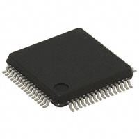


 工商网监
湘ICP备2023018690号
工商网监
湘ICP备2023018690号
