STB45N60DM2AG
Datasheet
Automotive-grade N-channel 600 V, 85 mΩ typ., 34 A MDmesh DM2
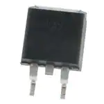
Power MOSFET in a D²PAK package
Features
TAB
2
1
Order code
VDS @ TJ max.
RDS(on) max.
ID
PTOT
STB45N60DM2AG
650 V
93 mΩ
34 A
250 W
3
•
•
•
•
•
•
•
D²PAK
D(2, TAB)
G(1)
AEC-Q101 qualified
Fast-recovery body diode
Extremely low gate charge and input capacitance
Low on-resistance
100% avalanche tested
Extremely high dv/dt ruggedness
Zener-protected
Applications
S(3)
AM01476v1_tab
•
Switching applications
Description
This high-voltage N-channel Power MOSFET is part of the MDmesh DM2 fastrecovery diode series. It offers very low recovery charge (Qrr) and time (trr) combined
with low RDS(on), rendering it suitable for the most demanding high-efficiency
converters and ideal for bridge topologies and ZVS phase-shift converters.
Product status link
STB45N60DM2AG
Product summary
Order code
STB45N60DM2AG
Marking
45N60DM2
Package
D²PAK
Packing
Tape and reel
DS11105 - Rev 2 - August 2021
For further information contact your local STMicroelectronics sales office.
www.st.com
�STB45N60DM2AG
Electrical ratings
1
Electrical ratings
Table 1. Absolute maximum ratings
Symbol
Value
Unit
Gate-source voltage
±25
V
Drain current (continuous) at TC = 25 °C
34
Drain current (continuous) at TC = 100 °C
21
IDM(1)
Drain current (pulsed)
136
A
PTOT
Total power dissipation at TC = 25 °C
250
W
dv/dt(2)
Peak diode recovery voltage slope
50
V/ns
dv/dt(3)
MOSFET dv/dt ruggedness
50
V/ns
Tstg
Storage temperature range
VGS
ID
TJ
Parameter
Operating junction temperature range
-55 to 150
A
°C
°C
1. Pulse width is limited by safe operating area.
2. ISD ≤ 34 A, di/dt = 800 A/μs, VDS (peak) < V(BR)DSS, VDD = 80% V(BR)DSS.
3. VDS ≤ 480 V.
Table 2. Thermal data
Symbol
RthJC
(1)
RthJB
Parameter
Value
Unit
Thermal resistance, junction-to-case
0.50
°C/W
Thermal resistance, junction-to-board
30
°C/W
Value
Unit
6
A
800
mJ
1. When mounted on a 1-inch² FR-4, 2 Oz copper board.
Table 3. Avalanche characteristics
Symbol
IAR
EAS(1)
Parameter
Avalanche current, repetitive or not repetitive
Single pulse avalanche energy
1. Starting TJ = 25 °C, ID = IAR, VDD = 50 V.
DS11105 - Rev 2
page 2/15
�STB45N60DM2AG
Electrical characteristics
2
Electrical characteristics
TC = 25 °C unless otherwise specified.
Table 4. Static
Symbol
V(BR)DSS
Parameter
Test conditions
Drain-source breakdown voltage
Min.
VGS = 0 V, ID = 1 mA
Typ.
600
Zero gate voltage drain current
IGSS
Gate-body leakage current
VDS = 0 V, VGS = ±25 V
VGS(th)
Gate threshold voltage
VDS = VGS, ID = 250 µA
RDS(on)
Static drain-source on-resistance
VGS = 10 V, ID = 17 A
VGS = 0 V, VDS = 600 V, TC = 125
Unit
V
VGS = 0 V, VDS = 600 V
IDSS
Max.
1
°C(1)
100
µA
±5
µA
4
5
V
85
93
mΩ
Min.
Typ.
Max.
Unit
-
2500
-
pF
-
120
-
pF
-
3
-
pF
3
1. Defined by design, not subject to production test.
Table 5. Dynamic
Symbol
Parameter
Test conditions
Ciss
Input capacitance
Coss
Output capacitance
Crss
Reverse transfer capacitance
Coss eq. (1)
Equivalent output capacitance
VDS = 0 to 480 V, VGS = 0 V
-
200
-
pF
RG
Intrinsic gate resistance
f = 1 MHz, ID = 0 A
-
4
-
Ω
Qg
Total gate charge
-
56
-
nC
Qgs
Gate-source charge
-
13
-
nC
Qgd
Gate-drain charge
-
30
-
nC
VDS = 100 V, f = 1 MHz, VGS = 0 V
VDD = 480 V, ID = 34 A, VGS = 0 to 10 V
(see Figure 14. Test circuit for gate
charge behavior)
1. Coss eq. is defined as a constant equivalent capacitance giving the same charging time as Coss when VDS increases from 0
to 80% VDSS.
Table 6. Switching times
Symbol
td(on)
tr
td(off)
tf
DS11105 - Rev 2
Parameter
Test conditions
Min.
Typ.
Max.
Unit
Turn-on delay time
VDD = 300 V, ID = 25 A,
-
29
-
ns
Rise time
RG = 4.7 Ω, VGS = 10 V
-
27
-
ns
Turn-off delay time
(see Figure 13. Test circuit for
resistive load switching times and
Figure 18. Switching time waveform)
-
85
-
ns
-
6
-
ns
Fall time
page 3/15
�STB45N60DM2AG
Electrical characteristics
Table 7. Source-drain diode
Symbol
ISD
ISDM
(1)
VSD (2)
Parameter
Test conditions
Min.
Typ.
Max.
Unit
Source-drain current
-
34
A
Source-drain current (pulsed)
-
136
A
1.6
V
Forward on voltage
VGS = 0 V, ISD = 34 A
-
trr
Reverse recovery time
ISD = 34 A, di/dt = 100 A/µs,
-
120
ns
Qrr
Reverse recovery charge
VDD = 60 V
-
0.6
µC
IRRM
Reverse recovery current
(see Figure 15. Test circuit for inductive
load switching and diode recovery times)
-
10.4
A
trr
Reverse recovery time
ISD = 34 A, di/dt = 100 A/µs,
-
240
ns
Qrr
Reverse recovery charge
VDD = 60 V, TJ = 150 °C
-
2.4
µC
Reverse recovery current
(see Figure 15. Test circuit for inductive
load switching and diode recovery times)
-
20.5
A
IRRM
1. Pulse width is limited by safe operating area.
2. Pulse test: pulse duration = 300 µs, duty cycle 1.5%.
DS11105 - Rev 2
page 4/15
�STB45N60DM2AG
Electrical characteristics (curves)
2.1
Electrical characteristics (curves)
Figure 2. Thermal impedance
Figure 1. Safe operating area
GC20540
GIPG120615FQ6LPSOA
ID
(A)
100
)
on
S(
10 μs
100 μs
1 ms
D
101
O
lim per
ite ati
d on
by in
m th
ax is
. R ar
e
a
is
102
10-1
10-1
100
10 ms
TJ ≤ 150 °C,
TC = 25 °C,
Single pulse
101
VDS (V)
102
Figure 3. Output characteristics
ID
(A)
Figure 4. Transfer characteristics
ID
(A)
GIPG120615FQ6LPOCH
VGS = 9, 10 V
100
60
80
60
VGS = 7 V
40
40
20
20
VGS = 6 V
0
0
4
8
12
16
VDS (V)
Figure 5. Gate charge vs gate-source voltage
VDS
(V)
GIPG120615FQ6LFQVG
VDD = 480 V
ID = 34 A
600
500
VDS = 15 V
100
VGS = 8 V
80
GIPG120615FQ6LPTCH
VGS
(V)
12
VDS
10
400
8
300
6
200
4
100
2
0
3
4
5
6
7
8
9
VGS (V)
Figure 6. Static drain-source on-resistance
RDS(on)
(mΩ)
GIPG120615FQ6LFRID
VGS = 10 V
96
92
88
0
0
DS11105 - Rev 2
10
20
30
40
50
60
0
Qg (nC)
84
80
76
0
5
10
15
20
25
30
ID (A)
page 5/15
�STB45N60DM2AG
Electrical characteristics (curves)
Figure 8. Normalized gate threshold voltage vs
temperature
Figure 7. Capacitance variations
C
(pF)
GIPG120615FQ6LFCVR
VGS(th)
(norm.)
104
GIPG120615FQ6LPVTH
1.1
Ciss
103
ID = 250 µA
1.0
0.9
102
Coss
101
Crss
0.8
f = 1 MHz
100
10-1
100
0.7
101
VDS (V)
102
Figure 9. Normalized on-resistance vs temperature
RDS(on)
(norm.)
GIPG120615FQ6LPRON
2.2
0.6
-75
1.04
1.4
1.00
1.0
0.96
0.6
0.92
-25
25
75
125
TJ (°C)
Figure 11. Output capacitance stored energy
E OSS
(µJ)
GIPG120615FQ6LPEOS
75
V (BR)DSS
(norm.)
125
TJ (°C)
GIPG120615FQ6LPBDV
I D = 1 mA
1.08
VGS = 10 V
25
Figure 10. Normalized V(BR)DSS vs temperature
1.8
0.2
-75
-25
0.88
-75
-25
25
75
125
T j (°C)
Figure 12. Source- drain diode forward characteristics
VSD
(V)
GIPG120615FQ6LPSDF
1.1
16
TJ = -50 °C
1.0
12
0.9
TJ = 25 °C
0.8
8
0.7
TJ = 150 °C
4
0
0
DS11105 - Rev 2
0.6
100
200
300
400
500
600
V DS (V)
0.5
0
4
8
12 16 20 24 28 32 ISD (A)
page 6/15
�STB45N60DM2AG
Test circuits
3
Test circuits
Figure 13. Test circuit for resistive load switching times
Figure 14. Test circuit for gate charge behavior
VDD
12 V
2200
+ μF
3.3
μF
VDD
VD
VGS
1 kΩ
100 nF
RL
IG= CONST
VGS
RG
47 kΩ
+
pulse width
D.U.T.
2.7 kΩ
2200
μF
pulse width
D.U.T.
100 Ω
VG
47 kΩ
1 kΩ
AM01469v1
AM01468v1
Figure 15. Test circuit for inductive load switching and
diode recovery times
D
G
A
D.U.T.
S
25 Ω
A
L
A
VD
100 µH
fast
diode
B
B
B
3.3
µF
D
G
+
Figure 16. Unclamped inductive load test circuit
RG
1000
+ µF
2200
+ µF
VDD
3.3
µF
VDD
ID
D.U.T.
S
D.U.T.
Vi
_
pulse width
AM01471v1
AM01470v1
Figure 18. Switching time waveform
Figure 17. Unclamped inductive waveform
ton
V(BR)DSS
td(on)
toff
td(off)
tr
tf
VD
90%
90%
IDM
VDD
10%
0
ID
VDD
VGS
AM01472v1
0
VDS
10%
90%
10%
AM01473v1
DS11105 - Rev 2
page 7/15
�STB45N60DM2AG
Package information
4
Package information
In order to meet environmental requirements, ST offers these devices in different grades of ECOPACK packages,
depending on their level of environmental compliance. ECOPACK specifications, grade definitions and product
status are available at: www.st.com. ECOPACK is an ST trademark.
4.1
D²PAK (TO-263) type A2 package information
Figure 19. D²PAK (TO-263) type A2 package outline
0079457_A2_26
DS11105 - Rev 2
page 8/15
�STB45N60DM2AG
D²PAK (TO-263) type A2 package information
Table 8. D²PAK (TO-263) type A2 package mechanical data
Dim.
mm
Min.
Max.
A
4.40
4.60
A1
0.03
0.23
b
0.70
0.93
b2
1.14
1.70
c
0.45
0.60
c2
1.23
1.36
D
8.95
9.35
D1
7.50
7.75
8.00
D2
1.10
1.30
1.50
E
10.00
E1
8.70
8.90
9.10
E2
7.30
7.50
7.70
e
10.40
2.54
e1
4.88
5.28
H
15.00
15.85
J1
2.49
2.69
L
2.29
2.79
L1
1.27
1.40
L2
1.30
1.75
R
V2
DS11105 - Rev 2
Typ.
0.40
0°
8°
page 9/15
�STB45N60DM2AG
D²PAK (TO-263) type A2 package information
Figure 20. D²PAK (TO-263) recommended footprint (dimensions are in mm)
0079457_Rev26_footprint
DS11105 - Rev 2
page 10/15
�STB45N60DM2AG
D²PAK packing information
4.2
D²PAK packing information
Figure 21. D²PAK tape outline
DS11105 - Rev 2
page 11/15
�STB45N60DM2AG
D²PAK packing information
Figure 22. D²PAK reel outline
T
40mm min.
access hole
at slot location
B
D
C
N
A
G measured
at hub
Tape slot
in core for
tape start
2.5mm min.width
Full radius
AM06038v1
Table 9. D²PAK tape and reel mechanical data
Tape
Dim.
DS11105 - Rev 2
Reel
mm
mm
Dim.
Min.
Max.
Min.
Max.
A0
10.5
10.7
A
B0
15.7
15.9
B
1.5
D
1.5
1.6
C
12.8
D1
1.59
1.61
D
20.2
E
1.65
1.85
G
24.4
F
11.4
11.6
N
100
K0
4.8
5.0
T
P0
3.9
4.1
P1
11.9
12.1
Base quantity
1000
P2
1.9
2.1
Bulk quantity
1000
R
50
T
0.25
0.35
W
23.7
24.3
330
13.2
26.4
30.4
page 12/15
�STB45N60DM2AG
Revision history
Table 10. Document revision history
Date
Revision
02-Jul-2015
1
Changes
Initial release.
Updated Features in cover page.
09-Aug-2021
2
Updated Table 4. Static.
Updated Section 4 Package information.
Minor text changes.
DS11105 - Rev 2
page 13/15
�STB45N60DM2AG
Contents
Contents
1
Electrical ratings . . . . . . . . . . . . . . . . . . . . . . . . . . . . . . . . . . . . . . . . . . . . . . . . . . . . . . . . . . . . . . . . . .2
2
Electrical characteristics. . . . . . . . . . . . . . . . . . . . . . . . . . . . . . . . . . . . . . . . . . . . . . . . . . . . . . . . . . . 3
2.1
Electrical characteristics (curves) . . . . . . . . . . . . . . . . . . . . . . . . . . . . . . . . . . . . . . . . . . . . . . . . . 5
3
Test circuits . . . . . . . . . . . . . . . . . . . . . . . . . . . . . . . . . . . . . . . . . . . . . . . . . . . . . . . . . . . . . . . . . . . . . . .7
4
Package information. . . . . . . . . . . . . . . . . . . . . . . . . . . . . . . . . . . . . . . . . . . . . . . . . . . . . . . . . . . . . . .8
4.1
D²PAK (TO-263) type A2 package information . . . . . . . . . . . . . . . . . . . . . . . . . . . . . . . . . . . . . . 8
4.2
D²PAK packing information . . . . . . . . . . . . . . . . . . . . . . . . . . . . . . . . . . . . . . . . . . . . . . . . . . . . . 11
Revision history . . . . . . . . . . . . . . . . . . . . . . . . . . . . . . . . . . . . . . . . . . . . . . . . . . . . . . . . . . . . . . . . . . . . . . .13
DS11105 - Rev 2
page 14/15
�STB45N60DM2AG
IMPORTANT NOTICE – PLEASE READ CAREFULLY
STMicroelectronics NV and its subsidiaries (“ST”) reserve the right to make changes, corrections, enhancements, modifications, and improvements to ST
products and/or to this document at any time without notice. Purchasers should obtain the latest relevant information on ST products before placing orders. ST
products are sold pursuant to ST’s terms and conditions of sale in place at the time of order acknowledgement.
Purchasers are solely responsible for the choice, selection, and use of ST products and ST assumes no liability for application assistance or the design of
Purchasers’ products.
No license, express or implied, to any intellectual property right is granted by ST herein.
Resale of ST products with provisions different from the information set forth herein shall void any warranty granted by ST for such product.
ST and the ST logo are trademarks of ST. For additional information about ST trademarks, please refer to www.st.com/trademarks. All other product or service
names are the property of their respective owners.
Information in this document supersedes and replaces information previously supplied in any prior versions of this document.
© 2021 STMicroelectronics – All rights reserved
DS11105 - Rev 2
page 15/15
�


 工商网监
湘ICP备2023018690号
工商网监
湘ICP备2023018690号

