STD10P10F6
Datasheet
P-channel -100 V, 0.36 Ω typ., -10 A STripFET F6 Power MOSFET
in a DPAK package
Features
TAB
2 3
1
•
•
•
•
DPAK
D(2, TAB)
Order code
VDS
RDS(on) max.
ID
STD10P10F6
-100 V
0.18 Ω
-10 A
Very low on-resistance
Very low gate charge
High avalanche ruggedness
Low gate drive power loss
Applications
•
Switching applications
G(1)
Description
S(3)
AM11258v1
This device is a P-channel Power MOSFET developed using the STripFET F6
technology, with a new trench gate structure. The resulting Power MOSFET exhibits
very low RDS(on) in all packages.
Product status link
STD10P10F6
Product summary
Order code
STD10P10F6
Marking
10P10F6
Package
DPAK
Packing
Tape and reel
DS10343 - Rev 3 - April 2022
For further information contact your local STMicroelectronics sales office.
www.st.com
�STD10P10F6
Electrical ratings
1
Electrical ratings
Table 1. Absolute maximum ratings
Symbol
Parameter
Value
Unit
VDS
Drain-source voltage
-100
V
VGS
Gate-source voltage
±20
V
ID
Drain current (continuous) at TC = 25 °C
-10
A
ID
Drain current (continuous) at TC = 100 °C
-7.5
A
IDM (1)
Drain current (pulsed)
-40
A
PTOT
Total power dissipation at TC=25 °C
40
W
Tstg
Storage temperature range
- 55 to 175
°C
Value
Unit
Thermal resistance, junction-to-case
3.75
°C/W
Thermal resistance, junction-to-board
50
°C/W
TJ
Operating junction temperature range
1. Pulse width limited by safe operating area.
Table 2. Thermal data
Symbol
RthJC
RthJB
(1)
Parameter
1. When mounted on FR-4 board of 1inch², 2oz Cu t < 10 s.
DS10343 - Rev 3
page 2/16
�STD10P10F6
Electrical characteristics
2
Electrical characteristics
TC = 25 °C unless otherwise specified.
Table 3. On /off states
Symbol
V(BR)DSS
IDSS
IGSS
Parameter
Test conditions
Drain-source breakdown voltage
VGS = 0 V, ID = -250 μA
Zero gate voltage
VGS = 0 V, VDS = -100 V
drain current
VGS = 0 V, VDS = -100 V, TC = 125
Gate-body leakage
Min.
Typ.
-100
VGS(th)
Gate threshold voltage
VDS = VGS, ID = -250 µA
RDS(on)
Static drain-source on- resistance
VGS = -10 V, ID = -5 A
Unit
V
-1
µA
-10
µA
±100
nA
-4
V
0.136
0.18
Ω
Min.
Typ.
Max.
Unit
-
864
-
pF
-
45
-
pF
-
25
-
pF
-
16.5
-
nC
-
3.5
-
nC
-
3.8
-
nC
Min.
Typ.
Max.
Unit
-
10.5
-
ns
-
4.8
-
ns
-
24
-
ns
-
4.5
-
ns
Min.
Typ.
Max.
Unit
-1.1
V
°C(1)
VDS = 0 V, VGS = ±20 V
current
Max.
-2
1. Defined by design, not subject to production test.
Table 4. Dynamic
Symbol
Parameter
Ciss
Input capacitance
Coss
Output capacitance
Crss
Reverse transfer capacitance
Qg
Total gate charge
Qgs
Gate-source charge
Qgd
Gate-drain charge
Test conditions
VDS = -80 V, f = 1 MHz, VGS = 0 V
VDD = -80 V, ID = -10 A, VGS = -10 V
(see Figure 13. Gate charge test circuit)
Table 5. Switching on/off (inductive load)
Symbol
td(on)
tr
td(off)
tf
Parameter
Test conditions
Turn-on delay time
VDD = -80 V, ID = -5 A, RG = 4.7 Ω,
Rise time
VGS = -10 V (see Figure 12. Switching
times test circuit for resistive load)
Turn-off delay time
Fall time
Table 6. Source drain-diode
Symbol
VSD (1)
Parameter
Forward on voltage
trr
Reverse recovery time
Qrr
Reverse recovery charge
IRRM
Reverse recovery current
Test conditions
ISD = -5 A, VGS = 0 V
ISD = -10 A, di/dt = 100 A/µs, VDD = -80 V
(see Figure 14. Test circuit for inductive
load switching and diode recovery times)
-
26.5
ns
-
36.5
nC
-
-2.7
A
1. Pulsed: pulse duration = 300 µs, duty cycle 1.5%
DS10343 - Rev 3
page 3/16
�STD10P10F6
Electrical characteristics (curves)
2.1
Electrical characteristics (curves)
Note:
For the P-channel Power MOSFET, current and voltage polarities are reversed.
Figure 1. Safe operating area
Figure 2. Normalized transient thermal impedance
GIPG021020141123FSR
ID
(A)
GIPG021020141545FSR
K
δ= 0.5
0.2
is
ea )
ar on
s DS(
i
th R
in ax
n
tio y m
ra d b
e
e
p
O mit
Li
10
100µs
0.1
1ms
1
10ms
Tj=175°C
Tc=25°C
Single pulse
0.1
0.1
1
VDS(V)
10
Figure 3. Typical output characteristics
GIPG270520141052SA
ID (A)
VGS=7, 8, 9, 10V
25
20
SINGLE PULSE
10-2
10-5
10
10
5
VDS=16V
5
4V
12
VDS(V)
Figure 5. Typical gate charge characteristics
GIPG270520141105SA
VDD=80V
ID=10A
12
tp(s)
GIPG270520141058SA
ID
(A)
15
VGS
(V)
10-2
Figure 4. Typical transfer characteristics
15
8
10-3
20
5V
4
10-4
25
6V
0
0
0.05
0.02
0.01
10-1
0
2
3
4
5
6
7
9
8
VGS(V)
Figure 6. Typical drain-source on-resistance
GIPG270520141110SA
RDS(on)
(mΩ)
VGS=10V
135.5
10
135
8
134.5
6
134
4
133.5
2
0
DS10343 - Rev 3
0
5
10
15
20
Qg(nC)
133
1
2
3
4
5
ID(A)
page 4/16
�STD10P10F6
Electrical characteristics (curves)
Figure 8. Normalized gate threshold vs temperature
Figure 7. Typical capacitance characteristics
GIPG270520141143SA
C
(pF)
GIPG270520141144SA
VGS(th)
(norm)
ID=250µA
1.1
1000
1
Ciss
0.9
100
0.8
Coss
0.7
Crss
10
0
20
60
40
0.6
-75
VDS(V)
25
75
125
TJ(°C)
Figure 10. Normalized breakdown voltage vs temperature
Figure 9. Normalized on-resistance vs temperature
GIPG270520141149SA
RDS(on)
-25
GIPG270520141200SA
V(BR)DSS
(norm)
(norm)
ID=1mA
VGS=10V
2.5
1.08
2
1.04
1.5
1
1
0.96
0.5
0
-75
-25
25
75
0.92
-75
125 TJ(°C)
-25
25
75
125
TJ(°C)
Figure 11. Typical reverse diode forward characteristics
GIPG270520141210SA
VSD (V)
TJ=-55°C
0.9
0.8
TJ=25°C
0.7
0.6
TJ=150°C
0.5
0.4
DS10343 - Rev 3
0
0.5
1
1.5
2
2.5
3
ISD(A)
page 5/16
�STD10P10F6
Test circuits
3
Test circuits
Figure 12. Switching times test circuit for resistive load
Figure 13. Gate charge test circuit
Figure 14. Test circuit for inductive load switching and diode recovery times
DS10343 - Rev 3
page 6/16
�STD10P10F6
Package information
4
Package information
In order to meet environmental requirements, ST offers these devices in different grades of ECOPACK packages,
depending on their level of environmental compliance. ECOPACK specifications, grade definitions and product
status are available at: www.st.com. ECOPACK is an ST trademark.
4.1
DPAK (TO-252) type A package information
Figure 15. DPAK (TO-252) type A package outline
0068772_A_30
DS10343 - Rev 3
page 7/16
�STD10P10F6
DPAK (TO-252) type A package information
Table 7. DPAK (TO-252) type A mechanical data
Dim.
mm
Min.
Max.
A
2.20
2.40
A1
0.90
1.10
A2
0.03
0.23
b
0.64
0.90
b4
5.20
5.40
c
0.45
0.60
c2
0.48
0.60
D
6.00
6.20
D1
4.95
E
6.40
E1
4.60
4.70
4.80
e
2.159
2.286
2.413
e1
4.445
4.572
4.699
H
9.35
10.10
L
1.00
1.50
(L1)
2.60
2.80
3.00
L2
0.65
0.80
0.95
L4
0.60
R
V2
DS10343 - Rev 3
Typ.
5.10
5.25
6.60
1.00
0.20
0°
8°
page 8/16
�STD10P10F6
DPAK (TO-252) type A2 package information
4.2
DPAK (TO-252) type A2 package information
Figure 16. DPAK (TO-252) type A2 package outline
0068772_type-A2_rev31
DS10343 - Rev 3
page 9/16
�STD10P10F6
DPAK (TO-252) type A2 package information
Table 8. DPAK (TO-252) type A2 mechanical data
Dim.
mm
Min.
Max.
A
2.20
2.40
A1
0.90
1.10
A2
0.03
0.23
b
0.64
0.90
b4
5.20
5.40
c
0.45
0.60
c2
0.48
0.60
D
6.00
6.20
D1
4.95
E
6.40
E1
5.10
5.20
5.30
e
2.159
2.286
2.413
e1
4.445
4.572
4.699
H
9.35
10.10
L
1.00
1.50
L1
2.60
2.80
3.00
L2
0.65
0.80
0.95
L4
0.60
R
V2
DS10343 - Rev 3
Typ.
5.10
5.25
6.60
1.00
0.20
0°
8°
page 10/16
�STD10P10F6
DPAK (TO-252) type A2 package information
Figure 17. DPAK (TO-252) recommended footprint (dimensions are in mm)
FP_0068772_31
DS10343 - Rev 3
page 11/16
�STD10P10F6
DPAK (TO-252) packing information
4.3
DPAK (TO-252) packing information
Figure 18. DPAK (TO-252) tape outline
10 pitches cumulative
tolerance on tape +/- 0.2 mm
T
P0
Top cover
tape
P2
D
E
F
B1
K0
For machine ref. only
including draft and
radii concentric around B0
W
B0
A0
P1
D1
User direction of feed
R
Bending radius
User direction of feed
AM08852v1
DS10343 - Rev 3
page 12/16
�STD10P10F6
DPAK (TO-252) packing information
Figure 19. DPAK (TO-252) reel outline
T
40mm min.
access hole
at slot location
B
D
C
N
A
G measured
at hub
Tape slot
in core for
tape start
2.5mm min.width
Full radius
AM06038v1
Table 9. DPAK (TO-252) tape and reel mechanical data
Tape
Dim.
mm
mm
Dim.
Min.
Max.
A0
6.8
7
A
B0
10.4
10.6
B
1.5
12.1
C
12.8
1.6
D
20.2
G
16.4
50
B1
DS10343 - Rev 3
Reel
Min.
Max.
330
13.2
D
1.5
D1
1.5
E
1.65
1.85
N
F
7.4
7.6
T
K0
2.55
2.75
P0
3.9
4.1
Base qty.
2500
P1
7.9
8.1
Bulk qty.
2500
P2
1.9
2.1
R
40
T
0.25
0.35
W
15.7
16.3
18.4
22.4
page 13/16
�STD10P10F6
Revision history
Table 10. Document revision history
Date
Revision
20-May-2014
1
02-Oct-2014
2
Changes
First release.
Document status promoted from preliminary to production data
Added Section 2.1: "Electrical characteristics (curves)".
Updated Section 4.1 DPAK (TO-252) type A package information
26-Apr-2022
3
Added Section 4.2 DPAK (TO-252) type A2 package information
Minor text changes.
DS10343 - Rev 3
page 14/16
�STD10P10F6
Contents
Contents
1
Electrical ratings . . . . . . . . . . . . . . . . . . . . . . . . . . . . . . . . . . . . . . . . . . . . . . . . . . . . . . . . . . . . . . . . . .2
2
Electrical characteristics. . . . . . . . . . . . . . . . . . . . . . . . . . . . . . . . . . . . . . . . . . . . . . . . . . . . . . . . . . . 3
2.1
Electrical characteristics (curves) . . . . . . . . . . . . . . . . . . . . . . . . . . . . . . . . . . . . . . . . . . . . . . . . . 4
3
Test circuits . . . . . . . . . . . . . . . . . . . . . . . . . . . . . . . . . . . . . . . . . . . . . . . . . . . . . . . . . . . . . . . . . . . . . . .6
4
Package information. . . . . . . . . . . . . . . . . . . . . . . . . . . . . . . . . . . . . . . . . . . . . . . . . . . . . . . . . . . . . . .7
4.1
DPAK (TO-252) type A package information . . . . . . . . . . . . . . . . . . . . . . . . . . . . . . . . . . . . . . . . 7
4.2
DPAK (TO-252) type A2 package information . . . . . . . . . . . . . . . . . . . . . . . . . . . . . . . . . . . . . . . 9
4.3
DPAK (TO-252) packing information. . . . . . . . . . . . . . . . . . . . . . . . . . . . . . . . . . . . . . . . . . . . . . 12
Revision history . . . . . . . . . . . . . . . . . . . . . . . . . . . . . . . . . . . . . . . . . . . . . . . . . . . . . . . . . . . . . . . . . . . . . . .14
DS10343 - Rev 3
page 15/16
�STD10P10F6
IMPORTANT NOTICE – READ CAREFULLY
STMicroelectronics NV and its subsidiaries (“ST”) reserve the right to make changes, corrections, enhancements, modifications, and improvements to ST
products and/or to this document at any time without notice. Purchasers should obtain the latest relevant information on ST products before placing orders. ST
products are sold pursuant to ST’s terms and conditions of sale in place at the time of order acknowledgment.
Purchasers are solely responsible for the choice, selection, and use of ST products and ST assumes no liability for application assistance or the design of
purchasers’ products.
No license, express or implied, to any intellectual property right is granted by ST herein.
Resale of ST products with provisions different from the information set forth herein shall void any warranty granted by ST for such product.
ST and the ST logo are trademarks of ST. For additional information about ST trademarks, refer to www.st.com/trademarks. All other product or service names
are the property of their respective owners.
Information in this document supersedes and replaces information previously supplied in any prior versions of this document.
© 2022 STMicroelectronics – All rights reserved
DS10343 - Rev 3
page 16/16
�
很抱歉,暂时无法提供与“STD10P10F6”相匹配的价格&库存,您可以联系我们找货
免费人工找货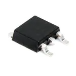


 工商网监
湘ICP备2023018690号
工商网监
湘ICP备2023018690号
