TDA2007A
®
6 + 6W STEREO AMPLIFIER
..
..
HIGH OUTPUT POWER
HIGH CURRENT CAPABILITY
AC SHORT CIRCUIT PROTECTION
THERMAL OVERLOAD PROTECTION
DESCRIPTION
The TDA2007A is a class AB dual Audio power amplifier assembled in single in line 9 pins package,
specially designed for stereo application in music
centers TV receivers and portable radios.
SIP9
c
u
d
ORDERING NUMBER : TDA2007A
e
t
le
STEREO TEST CIRCUIT
)
s
(
ct
)
s
t(
o
r
P
o
s
b
O
-
u
d
o
r
P
e
t
e
l
o
s
b
O
September 2003
1/7
�TDA2007A
PIN CONNECTION (top view)
c
u
d
e
t
le
SCHEMATIC DIAGRAM
)
s
(
ct
)
s
t(
o
r
P
o
s
b
O
-
u
d
o
r
P
e
t
e
l
o
s
b
O
THERMAL DATA
Symbol
Parameter
Rth j-case Thermal Resistance Junction-case
Rth j-amb Thermal Resistance Junctio-ambient
2/7
Max.
Max.
Value
8
70
Unit
°C/W
°C/W
�TDA2007A
ABSOLUTE MAXIMUM RATINGS
Symbol
Value
Unit
VS
IO
Supply Voltage
28
V
Output Peak Current (repetitive f ≥ 20Hz)
3
A
IO
Output Peak Current (non repetitive t = 100µs)
3.5
A
10
–40 to 150
W
°C
Ptot
Tstg, Tj
Parameter
Power Dissipation at Tcase = 70°C
Storage and Junction Temperature
ELECTRICAL CHARACTERISTICS (refer to the stereo application circuit, Tamb = 25°C, VS = 18V,
GV = 36dB, unless otherwise specified)
Symbol
Parameter
Test Condition
Min.
Typ.
Unit
26
V
VS
Supply Voltage
VO
Id
Quiescent Output Voltage
8.5
Total Quiescent Drain Curent
50
90
mA
PO
Output Power
(each channel)
6
6
uc
W
W
d
8
Max.
f = 100Hz to 6KHz
d = 0.5%
VS = 18V RL = 4Ω
VS = 22V RL = 8W
f = 1KHz, VS = 18V, RL = 4Ω
PO = 100mW to 3W
f = 1KHz, VS = 22V, RL = 8Ω
PO = 100mW to 3W
Distortion
(each channel)
RL = ∞, Rg = 10KΩ
f = 1KHz
f = 10KHz
Cross Talk (ooo)
CT
Vi
Input Saturation Voltage (rms)
Ri
fL
Input Resistance
Low Frequency Roll Off (–3dB)
fH
GV
Low Frequency Roll Off (–3dB)
Voltage Gain (closed loop)
∆GV
Closed Loop Gain Matching
SVR
Tj
o
r
P
e
Supply Voltage Rejection
(each channel)
Thermal Shut-down Junction
Temperature
t
e
l
o
(°) Curve A.
s
b
O
r
P
e
t
le
o
s
b
O
-
f = 1KHz
RL = 4Ω, C10 = C11 = 2200µF
(s)
ct
du
Total Input Noise Voltage
eN
5.5
5.5
f = 1KHz
50
40
V
od
0.1
%
0.05
%
60
50
dB
dB
300
mV
70
200
40
35.5
36
KΩ
Hz
80
KHz
36.5
0.5
o
)
s
t(
dB
dB
µV
µV
Rg = 10kΩ ( )
Rg = 10kΩ (oo)
1.5
2.5
Rg = 10KΩ
fripple = 100Hz, Vripple = 0.5V
55
dB
145
°C
8
(°°) 22Hz to 22KHz.
3/7
�TDA2007A
Figure 1 : Stereo Test Circuit (G V = 36 dB).
c
u
d
e
t
le
o
r
P
Figure 2 : P.C. Board and Components layout of the Circuit of Fig.1 (1 : 1 scale).
)
s
(
ct
u
d
o
r
P
e
t
e
l
o
s
b
O
4/7
o
s
b
O
-
)
s
t(
�TDA2007A
APPLICATION SUGGESTION
The recommended values of the components are those shown on application circuit of fig.1. Different values
can be used ; the following table can help the designer.
Component
Recommended value
R1, R3
1.3KΩ
R2 and R4
18Ω
R5 and R6
1Ω
C1 and C2
Purpose
Larger Than
Smaller Than
Close Loop Gain
Setting (*)
Increase of Gain
Decrease of Gain
Decrease of Gain
Increase of gain
Frequency stability
Danger of Oscillation
at High Frequency
with Inductive Load
2.2µF
Input DC Decoupling
High Turn-on Delay
High Turn-on Pop
Higher Low Frequency
Cutoff. Increase of
Noise
C3
22µF
Ripple Rejection
Better SVR Increase
of the Switch-on Time
Degradation of SVR
C6 and C7
220µF
Feedback Input DC
Decoupling
C8 and C9
0.1µF
Frequency Stability
C10 and C11
1000µF to 2200µF
c
u
d
Output DC Decoupling
Higher Low-frequency
Cut-off
(*) The closed loop gain must be higher than 26 dB.
e
t
le
APPLICATION INFORMATION
o
r
P
o
s
b
O
-
Figure 3 : 12 W Bridge Amplifier (d = 0.5%, G V = 40 dB).
)
s
(
ct
)
s
t(
Danger of Oscillation
u
d
o
r
P
e
t
e
l
o
s
b
O
5/7
�TDA2007A
mm
MIN.
inch
TYP.
MAX.
A
MIN.
TYP.
7.1
2.7
3
0.280
0.106
0.118
B
23
0.90
B3
24.8
0.976
b1
0.5
b3
0.020
0.85
1.6
0.033
0.063
C
3.3
0.130
c1
0.43
0.017
c2
1.32
0.052
D
21.2
0.835
d1
14.5
0.571
e
2.54
0.100
e3
20.32
L
0.800
3.1
0.122
L1
3
0.118
L2
17.6
0.693
L3
0.25
L4
17.4
17.85
M
3.2
N
1
0.685
0,702
0.006
D
L1
)
s
(
ct
a1
1
o
r
P
SIP9
C
c2
N
M
A
o
r
P
e
du
o
s
b
O
-
)
s
t(
9
L
L2
P
L4
e
t
le
0.039
0.15
t
e
l
o
c
u
d
0.010
0.126
P
s
b
O
Weight: 1.87gr
d1
a1
OUTLINE AND
MECHANICAL DATA
MAX.
L3
DIM.
b1
b3
e
c
1
e3
B
B3
SIP9
0016107 D
6/7
�TDA2007A
c
u
d
e
t
le
)
s
(
ct
)
s
t(
o
r
P
o
s
b
O
-
u
d
o
r
P
e
t
e
l
o
Information furnished is believed to be accurate and reliable. However, STMicroelectronics assumes no responsibility for the consequences of use of such information nor for any infringement of patents or other rights of third parties which may result from its use. No
license is granted by implication or otherwise under any patent or patent rights of STMicroelectronics. Specifications mentioned in this
publication are subject to change without notice. This publication supersedes and replaces all information previously supplied. STMicroelectronics products are not authorized for use as critical components in life support devices or systems without express written
approval of STMicroelectronics.
s
b
O
The ST logo is a registered trademark of STMicroelectronics.
All other names are the property of their respective owners
© 2003 STMicroelectronics - All rights reserved
STMicroelectronics GROUP OF COMPANIES
Australia – Belgium - Brazil - Canada - China – Czech Republic - Finland - France - Germany - Hong Kong - India - Israel - Italy - Japan Malaysia - Malta - Morocco - Singapore - Spain - Sweden - Switzerland - United Kingdom - United States
www.st.com
7/7
�
很抱歉,暂时无法提供与“TDA2007A”相匹配的价格&库存,您可以联系我们找货
免费人工找货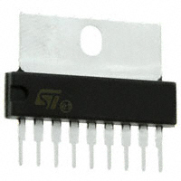


 工商网监
湘ICP备2023018690号
工商网监
湘ICP备2023018690号
