TXDVxx12
12 A high voltage Triacs
Features
A2
■
On-state current (IT(RMS)): 12 A
■
Max. blocking voltage (VDRM/VRRM): 1200 V
■
Gate current (IGT): 100 mA
■
Commutation @ 10 V/µs: up to 42.5 A/ms
■
Noise immunity: 2 kV/µs
■
Insulated package:
– 2,500 V rms (UL recognized: E81734).
G
A1
Description
A1
A2
The TXDVxx12 series uses a high performance
alternistor technology.
TO-220AB
insulated
Featuring very high commutation levels and high
surge current capability, these devices are well
adapted to power control for inductive and
resistive loads (motor, transformer...) especially
on three-phase power grid. Targeted three-phase
applications include heating systems, motor
starters, and induction motor speed control
(especially for fans).
Table 1.
G
Device summary
Parameter
Blocking voltage VDRM/VRRM
TXDV812RG
TXDV1212RG
800 V
1200 V
On-state current IT(RMS)
12 A
100 mA
Gate current IGT
January 2012
Doc ID 18272 Rev 2
1/7
www.st.com
7
�Characteristics
TXDVxx12
1
Characteristics
Table 2.
Absolute maximum ratings (limiting values)
Symbol
Parameter
IT(RMS)
On-state rms current (180° conduction angle)
VDRM
VRRM
Repetitive peak off-state voltage
Value
Unit
12
A
800
V
Tc = 90 °C
TXDV812
TXDV1212
Tj = 125 °C
1200
tp = 2.5 ms
ITSM
I2t
Non repetitive surge peak on-state current
I2t
value for fusing
dI/dt
Critical rate of rise of on-state current
IG = 500 mA dIG/dt = 1 A/µs
Tstg
Tj
Storage junction temperature range
Operating junction temperature range
tp = 8.3 ms
170
Tj = 25 °C
125
A
tp = 10 ms
120
tp = 10 ms
72
A2 S
F = 50 Hz
100
A/µs
- 40 to + 150
- 40 to + 125
°C
2500
V
VINS(RMS)(1) Insulation rms voltage
1. A1, A2, gate terminals to case for 1 minute
Table 3.
Electrical characteristics (Tj = 25 °C, unless otherwise specified)
Value
Symbol
Test conditions
TXDV812
IGT
VGT
VGD
VD = 12 V DC, RL = 33 Ω
VD = VDRM
RL = 3.3 kΩ
Tj = 110 °C
tgt
VD = VDRM IG = 500 mA dIG/dt = 3 A/µs
IL
IG = 1.2 x IGT
IH (1)
IT = 500 mA
dV/dt (1)
VTM
(1)
ITM = 17 A
Vto
(1)
Rd
(1)
IDRM
IRRM
MAX.
100
mA
I-II-III
MAX.
1.5
V
I-II-III
MIN.
0.2
V
I-II-III
TYP.
2.5
µs
II
Gate open
(dI/dt)c (1) (dV/dt)c = 10 V/µs
100
TYP.
mA
200
MAX.
100
mA
Tj = 125 °C
MIN.
2
kV/µs
Tj = 110 °C
MIN.
tp = 380 µs
42.5
30
A/ms
MAX.
1.95
V
Threshold voltage
MAX.
1.21
V
Dynamic resistance
MAX.
40
mΩ
VDRM = VRRM
Tj = 25 °C
Tj = 110 °C
1. For either polarity of electrode A2 voltage with reference to electrode A1.
2/7
TXDV1212
I-II-III
I-III
Linear slope up to:
VD = 67% VDRM Gate open
Unit
Quadrant
Doc ID 18272 Rev 2
MAX.
0.01
2
5
mA
�TXDVxx12
Characteristics
Table 4.
Gate characteristics (maximum values)
Symbol
Parameter
PG(AV)
Value
Unit
1
W
Average gate power dissipation
PGM
Peak gate power dissipation
tp = 20 µs
10
W
IGM
Peak gate current
tp = 20 µs
4
A
VGM
Peak positive gate voltage
tp = 20 µs
16
V
Value
Unit
Junction to ambient
60
°C/W
Rth(j-c) DC
Junction to case for DC
2.5
°C/W
Rth(j-c) AC
Junction to case for 360 °Conduction angle (F = 50 Hz)
1.9
°C/W
Table 5.
Thermal resistance
Symbol
Parameter
Rth(j-a)
Figure 1.
Max. rms power dissipation versus Figure 2.
on-state rms current (F = 50Hz).
(curves limited by (dI/dt)c)
Max. rms power dissipation and
max. allowable temperatures
(Tamb and Tcase) for various Rth
P(W)
P(W)
20
Tcase(° C)
20
18
18
α = 180°
16
Rth case to ambient
Rth = 0° C/W
1° C/W
2° C/W
4° C/W
16
α = 120°
14
12
6
α = 30°
180°
α
α
IT(RMS)(A)
1
2
Figure 3.
3
4
5
6
8
-110
6
-115
4
-120
2
0
0
-105
10
α = 60°
2
-100
12
10
4
-95
14
α = 90°
8
-90
7
8
9
10
11
12
On-state rms current versus case
temperature
Tamb(° C)
-125
0
0
20
Figure 4.
40
60
80
100
120
140
Relative variation of thermal
impedance versus pulse duration
Zth/Rth
IT(RMS)(A)
14
1
12
Zth(j-c)
10
α = 180°
8
Zth(j-a)
0.1
6
4
2
TC(°C)
tp(s)
0
0.01
0
10
20
30
40
50
60
70
80
90
100 110 120 130
1E-3
Doc ID 18272 Rev 2
1E-2
1E-1
1E+0
1E+1
1E+2
5E+2
3/7
�Characteristics
Figure 5.
TXDVxx12
Relative variation of gate trigger
Figure 6.
current and holding current versus
junction temperature
Non repetitive surge peak on-state
current versus number of cycles
ITSM(A)
IGT[Tj]
. IH[Tj]
IGT[Tj=25°C] IH[Tj=25°C]
120
2.5
100
t = 20 ms
2.0
One cycle
80
1.5
IGT
60
IH
Tj initial=25°C
1.0
40
0.5
20
Tj(°C)
0.0
-40 -30 -20 -10
Figure 7.
0
10
20
30
40
Number of cycles
50
60
70
80
0
90 100 110
0
10
Non-repetitive surge peak on-state Figure 8.
current for a sinusoidal pulse and
corresponding values of I2t
100
1000
On-state characteristics (maximum
values)
ITM(A)
ITSM(A), I2t (A2s)
1000
Tj max.:
Vt0=1.21V
Rt=0.040Ω
Tj initial = 25°C
ITSM
100
Tj initial = 25° C
100
I2t
10
Tj max.
VTM(V)
tp(ms)
1
10
1
Figure 9.
2
5
10
1
2
Safe turn-off operating area
(dV/dt)c(V/µs)
1000
Tj = 110° C
100
10
(dI/dt)c(A/ms)
1
1
4/7
10
Doc ID 18272 Rev 2
100
3
4
5
6
�TXDVxx12
2
Package information
Package information
●
Epoxy meets UL94,V0
●
Cooling method: C (by conduction)
●
Recommended torque value: 0.4 to 0.6 N·m
In order to meet environmental requirements, ST offers these devices in different grades of
ECOPACK® packages, depending on their level of environmental compliance. ECOPACK®
specifications, grade definitions and product status are available at: www.st.com.
ECOPACK® is an ST trademark.
Table 6.
TO-220AB insulated dimensions
Dimensions
Ref.
Millimeters
Min.
A
15.20
a1
C
B
ØI
F
A
Max.
Min.
Typ.
15.90 0.598
3.75
Max.
0.625
0.147
a2
13.00
14.00 0.511
0.551
B
10.00
10.40 0.393
0.409
b1
0.61
0.88
0.024
0.034
b2
1.23
1.32
0.048
0.051
C
4.40
4.60
0.173
0.181
c1
0.49
0.70
0.019
0.027
c2
2.40
2.72
0.094
0.107
e
2.40
2.70
0.094
0.106
F
6.20
6.60
0.244
0.259
ØI
3.75
3.85
0.147
0.151
I4
15.80 16.40 16.80 0.622 0.646 0.661
L
2.65
2.95
0.104
0.116
l2
1.14
1.70
0.044
0.066
l3
1.14
1.70
0.044
0.066
b2
L
Typ.
Inches
I4
l3
c2
a1
l2
a2
M
b1
c1
e
M
Doc ID 18272 Rev 2
2.60
0.102
5/7
�Ordering information
3
Ordering information
Table 7.
4
Ordering information
Order code
Marking
Package
Weight
TXDV812RG
TXDV812
TXDV1212
TO-220AB
insulated
2.3 g
TXDV1212RG
Base qty Delivery mode
50
Revision history
Table 8.
6/7
TXDVxx12
Document revision history
Date
Revision
Changes
30-Mar-2011
1
Initial release.
13-Jan-2012
2
Updated dI/dt in Table 2, and added Vto and Rd in Table 3
Doc ID 18272 Rev 2
Tube
�TXDVxx12
Please Read Carefully:
Information in this document is provided solely in connection with ST products. STMicroelectronics NV and its subsidiaries (“ST”) reserve the
right to make changes, corrections, modifications or improvements, to this document, and the products and services described herein at any
time, without notice.
All ST products are sold pursuant to ST’s terms and conditions of sale.
Purchasers are solely responsible for the choice, selection and use of the ST products and services described herein, and ST assumes no
liability whatsoever relating to the choice, selection or use of the ST products and services described herein.
No license, express or implied, by estoppel or otherwise, to any intellectual property rights is granted under this document. If any part of this
document refers to any third party products or services it shall not be deemed a license grant by ST for the use of such third party products
or services, or any intellectual property contained therein or considered as a warranty covering the use in any manner whatsoever of such
third party products or services or any intellectual property contained therein.
UNLESS OTHERWISE SET FORTH IN ST’S TERMS AND CONDITIONS OF SALE ST DISCLAIMS ANY EXPRESS OR IMPLIED
WARRANTY WITH RESPECT TO THE USE AND/OR SALE OF ST PRODUCTS INCLUDING WITHOUT LIMITATION IMPLIED
WARRANTIES OF MERCHANTABILITY, FITNESS FOR A PARTICULAR PURPOSE (AND THEIR EQUIVALENTS UNDER THE LAWS
OF ANY JURISDICTION), OR INFRINGEMENT OF ANY PATENT, COPYRIGHT OR OTHER INTELLECTUAL PROPERTY RIGHT.
UNLESS EXPRESSLY APPROVED IN WRITING BY TWO AUTHORIZED ST REPRESENTATIVES, ST PRODUCTS ARE NOT
RECOMMENDED, AUTHORIZED OR WARRANTED FOR USE IN MILITARY, AIR CRAFT, SPACE, LIFE SAVING, OR LIFE SUSTAINING
APPLICATIONS, NOR IN PRODUCTS OR SYSTEMS WHERE FAILURE OR MALFUNCTION MAY RESULT IN PERSONAL INJURY,
DEATH, OR SEVERE PROPERTY OR ENVIRONMENTAL DAMAGE. ST PRODUCTS WHICH ARE NOT SPECIFIED AS "AUTOMOTIVE
GRADE" MAY ONLY BE USED IN AUTOMOTIVE APPLICATIONS AT USER’S OWN RISK.
Resale of ST products with provisions different from the statements and/or technical features set forth in this document shall immediately void
any warranty granted by ST for the ST product or service described herein and shall not create or extend in any manner whatsoever, any
liability of ST.
ST and the ST logo are trademarks or registered trademarks of ST in various countries.
Information in this document supersedes and replaces all information previously supplied.
The ST logo is a registered trademark of STMicroelectronics. All other names are the property of their respective owners.
© 2012 STMicroelectronics - All rights reserved
STMicroelectronics group of companies
Australia - Belgium - Brazil - Canada - China - Czech Republic - Finland - France - Germany - Hong Kong - India - Israel - Italy - Japan Malaysia - Malta - Morocco - Philippines - Singapore - Spain - Sweden - Switzerland - United Kingdom - United States of America
www.st.com
Doc ID 18272 Rev 2
7/7
�
很抱歉,暂时无法提供与“TXDV812RG”相匹配的价格&库存,您可以联系我们找货
免费人工找货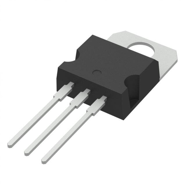


 工商网监
湘ICP备2023018690号
工商网监
湘ICP备2023018690号
