TYN640, TYN840
40 A standard SCRs
Datasheet - production data
Description
A
These standard SCRs are suitable for
applications where in-rush current conditions are
critical, such as overvoltage crowbar protection
circuits in power supplies, in-rush current limiting
circuits, solid state relays (in back to back
configuration), welding equipment, high power
motor control circuits.
G
Using clip assembly technology, they provide a
superior performance in high surge current
capabilities.
K
A
Table 1. Device summary
K
A
G
Order code
Voltage
Sensitivity
TYN640RG
600 V
35 mA
TYN840RG
800 V
35 mA
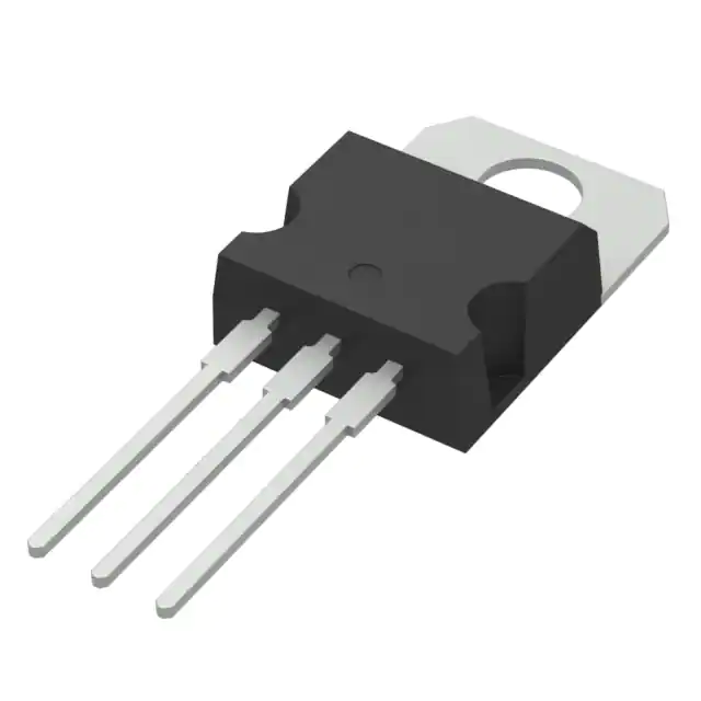
TO-220AB
Features
On-state rms current, IT(RMS): 40 A
Repetitive peak off-stat voltage, VDRM, VRRM:
– 600 V
– 800 V
Triggering gate current, IGT: 35 mA
November 2013
This is information on a product in full production.
DocID6944 Rev 6
1/8
www.st.com
�Characteristics
1
TYN640, TYN840
Characteristics
Table 2. Absolute ratings (limiting values)
Symbol
Parameter
Value
Unit
On-state rms current (180° conduction angle)
Tc = 95 °C
40
A
IT(AV)
Average on-state current (180° conduction angle)
Tc = 95 °C
25
A
ITSM
Non repetitive surge peak on-state
current
IT(RMS)
I²t
I²t Value for fusing
tp = 8.3 ms
tp = 10 ms
tp = 10 ms
480
Tj = 25 °C
Tj = 25 °C
A
460
1060
A2S
dI/dt
Critical rate of rise of on-state current
F = 60 Hz
IG = 2 x IGT, tr 100 ns
Tj = 125
°C
50
A/µs
IGM
Peak gate current
Tj = 125
°C
4
A
Tj = 125
°C
1
W
PG(AV)
tp = 20 µs
Average gate power dissipation
Tstg
Tj
Storage junction temperature range
Operating junction temperature range
- 40 to + 150
- 40 to + 125
°C
VRGM
Maximum peak reverse gate voltage
5
V
Table 3. Electrical Characteristics (Tj = 25 °C, unless otherwise specified)
Symbol
IGT
Test Conditions
Value
VGT
VGD
VD = VDRM
RL = 3.3 kΩ
IH
IT = 500 mA
Gate open
IL
IG = 1.2 x IGT
MIN.
3.5
MAX.
35
MAX.
1.3
V
MIN.
0.2
V
MAX.
75
mA
MAX.
150
mA
mA
RL = 33 Ω
VD = 12 V
Unit
Tj = 125 °C
dV/dt
VD = 67% VDRM Gate open
Tj = 125 °C
MIN.
1000
V/µs
VTM
ITM = 80 A
Tj = 25 °C
MAX.
1.6
V
Vt0
Threshold voltage
Tj = 125 °C
MAX.
0.85
V
Rd
Dynamic resistance
Tj = 125 °C
MAX.
10
mΩ
5
µA
4
mA
Value
Unit
IDRM
IRRM
tp = 380 µs
Tj = 25 °C
VDRM = VRRM
Tj = 125 °C
MAX.
Table 4. Thermal resistance
Symbol
2/8
Parameter
Rth(j-c)
Junction to case (DC)
0.8
°C/W
Rth(j-a)
Junction to ambient (DC)
60
°C/W
DocID6944 Rev 6
�TYN640, TYN840
Characteristics
Figure 1. Maximum average power dissipation
versus average on-state current
Figure 2. Average and DC on-state current
versus case temperature
IT(AV)(A)
P(W)
50
40
α = 180°
35
DC
40
30
25
30
α = 180°
20
20
15
360°
10
10
5
α
IT(AV)(A)
Tcase(°C)
0
0
0
5
10
15
20
25
30
Figure 3. Relative variation of thermal
impedance versus pulse duration
0
25
50
75
100
125
Figure 4. Relative variation of gate trigger
current, holding current and latching current
versus junction temperature
K=[Zth/Rth]
IGT,IH,IL[Tj] / IGT,IH,IL[Tj=25°C]
1.00
2.5
Zth(j-c)
2.0
1.5
0.10
IGT
Zth(j-a)
1.0
IH & IL
0.5
tp(s)
Tj(°C)
0.01
1E-3
1E-2
1E-1
1E+0
1E+1
1E+2
5E+2
0.0
-40
DocID6944 Rev 6
-20
0
20
40
60
80
100
120
140
3/8
8
�Characteristics
TYN640, TYN840
Figure 5. Surge peak on-state current versus
number of cycles
500
Figure 6. Non-repetitive surge peak on-state
current for a sinusoidal pulse with width
tp < 10 ms, and corresponding values of I²t
ITSM(A)
ITSM(A), I2t (A2s)
5000
450
Tj initial = 25°C
tp=10ms
400
350
One cycle
Non repetitive
Tj initial=25 °C
300
ITSM
I2t
1000
250
200
150
dI/dt limitation
100
Repetitive
TC=95°C
50
tp(ms)
Number of cycles
100
0
1
10
100
0.01
1000
0.10
1.00
Figure 7. On-state characteristics (maximum values)
ITM(A)
500
Tj max.:
Vt0=0.85V
Rd=10mΩ
100
Tj=max
10
Tj=25°C
VTM(V)
1
0.0
4/8
0.5
1.0
1.5
2.0
2.5
3.0
DocID6944 Rev 6
3.5
4.0
4.5
5.0
10.00
�TYN640, TYN840
2
Package information
Package information
Epoxy meets UL94, V0
Lead-free package
In order to meet environmental requirements, ST offers these devices in different grades of
ECOPACK® packages, depending on their level of environmental compliance. ECOPACK®
specifications, grade definitions and product status are available at: www.st.com.
ECOPACK® is an ST trademark.
Figure 8. TO-220AB dimension definitions
C
B
ØI
b2
L
F
A
I4
l3
c2
a1
l2
a2
M
b1
c1
e
DocID6944 Rev 6
5/8
8
�Package information
Table 5.
TYN640, TYN840
TO-220AB dimension values
Dimensions
Ref.
Millimeters
Min.
A
15.20
a1
Max.
Min.
15.90
0.598
3.75
Typ.
Max.
0.625
0.147
a2
13.00
14.00
0.511
0.551
B
10.00
10.40
0.393
0.409
b1
0.61
0.88
0.024
0.034
b2
1.23
1.32
0.048
0.051
C
4.40
4.60
0.173
0.181
c1
0.49
0.70
0.019
0.027
c2
2.40
2.72
0.094
0.107
e
2.40
2.70
0.094
0.106
F
6.20
6.60
0.244
0.259
ØI
3.75
3.85
0.147
0.151
I4
15.80
16.80
0.622
L
2.65
2.95
0.104
0.116
l2
1.14
1.70
0.044
0.066
l3
1.14
1.70
0.044
0.066
M
6/8
Typ.
Inches
16.40
2.60
DocID6944 Rev 6
0.646
0.102
0.661
�TYN640, TYN840
3
Ordering information
Ordering information
Figure 9. Ordering Information Scheme
TYN
x
40
RG
Standard SCR series
Voltage
6 = 600V
8 = 800V
Current
40 = 40A
Packing mode
RG = Tube
Table 6. Ordering Information
4
Ordering type
Marking
TYN640RG
TYN640
TYN840RG
TYN840
Package
Weight
TO-220AB
2.3 g
Base qty Delivery mode
50
Tube
Revision history
Table 7. Document revision history
Date
Revision
Changes
Apr-2002
4A
13-Feb-2006
5
TO-220AB delivery mode changed from bulk to tube.
ECOPACK statement added.
05-Nov-2013
6
Updated Figure 5.
Last update.
DocID6944 Rev 6
7/8
8
�TYN640, TYN840
Please Read Carefully:
Information in this document is provided solely in connection with ST products. STMicroelectronics NV and its subsidiaries (“ST”) reserve the
right to make changes, corrections, modifications or improvements, to this document, and the products and services described herein at any
time, without notice.
All ST products are sold pursuant to ST’s terms and conditions of sale.
Purchasers are solely responsible for the choice, selection and use of the ST products and services described herein, and ST assumes no
liability whatsoever relating to the choice, selection or use of the ST products and services described herein.
No license, express or implied, by estoppel or otherwise, to any intellectual property rights is granted under this document. If any part of this
document refers to any third party products or services it shall not be deemed a license grant by ST for the use of such third party products
or services, or any intellectual property contained therein or considered as a warranty covering the use in any manner whatsoever of such
third party products or services or any intellectual property contained therein.
UNLESS OTHERWISE SET FORTH IN ST’S TERMS AND CONDITIONS OF SALE ST DISCLAIMS ANY EXPRESS OR IMPLIED
WARRANTY WITH RESPECT TO THE USE AND/OR SALE OF ST PRODUCTS INCLUDING WITHOUT LIMITATION IMPLIED
WARRANTIES OF MERCHANTABILITY, FITNESS FOR A PARTICULAR PURPOSE (AND THEIR EQUIVALENTS UNDER THE LAWS
OF ANY JURISDICTION), OR INFRINGEMENT OF ANY PATENT, COPYRIGHT OR OTHER INTELLECTUAL PROPERTY RIGHT.
ST PRODUCTS ARE NOT DESIGNED OR AUTHORIZED FOR USE IN: (A) SAFETY CRITICAL APPLICATIONS SUCH AS LIFE
SUPPORTING, ACTIVE IMPLANTED DEVICES OR SYSTEMS WITH PRODUCT FUNCTIONAL SAFETY REQUIREMENTS; (B)
AERONAUTIC APPLICATIONS; (C) AUTOMOTIVE APPLICATIONS OR ENVIRONMENTS, AND/OR (D) AEROSPACE APPLICATIONS
OR ENVIRONMENTS. WHERE ST PRODUCTS ARE NOT DESIGNED FOR SUCH USE, THE PURCHASER SHALL USE PRODUCTS AT
PURCHASER’S SOLE RISK, EVEN IF ST HAS BEEN INFORMED IN WRITING OF SUCH USAGE, UNLESS A PRODUCT IS
EXPRESSLY DESIGNATED BY ST AS BEING INTENDED FOR “AUTOMOTIVE, AUTOMOTIVE SAFETY OR MEDICAL” INDUSTRY
DOMAINS ACCORDING TO ST PRODUCT DESIGN SPECIFICATIONS. PRODUCTS FORMALLY ESCC, QML OR JAN QUALIFIED ARE
DEEMED SUITABLE FOR USE IN AEROSPACE BY THE CORRESPONDING GOVERNMENTAL AGENCY.
Resale of ST products with provisions different from the statements and/or technical features set forth in this document shall immediately void
any warranty granted by ST for the ST product or service described herein and shall not create or extend in any manner whatsoever, any
liability of ST.
ST and the ST logo are trademarks or registered trademarks of ST in various countries.
Information in this document supersedes and replaces all information previously supplied.
The ST logo is a registered trademark of STMicroelectronics. All other names are the property of their respective owners.
© 2013 STMicroelectronics - All rights reserved
STMicroelectronics group of companies
Australia - Belgium - Brazil - Canada - China - Czech Republic - Finland - France - Germany - Hong Kong - India - Israel - Italy - Japan Malaysia - Malta - Morocco - Philippines - Singapore - Spain - Sweden - Switzerland - United Kingdom - United States of America
www.st.com
8/8
DocID6944 Rev 6
�


 工商网监
湘ICP备2023018690号
工商网监
湘ICP备2023018690号

