UPSD3422 UPSD3433
UPSD3434 UPSD3454
Turbo Plus series
Fast Turbo 8032 MCU with USB and programmable logic
Features
■
Fast 8-bit Turbo 8032 MCU, 40 MHz
– Advanced core, 4-clocks per instruction
– 10 MIPs peak performance at 40 MHz (5 V)
– JTAG debug and in-system programming
– 16-bit internal instruction path fetches
double-byte instruction in a single memory
cycle
– Branch cache & 4 instruction prefetch
queue
– Dual XDATA pointers with automatic
increment and decrement
– Compatible with 3rd party 8051 tools
)
s
(
t
c
u
d
o
)
r
s
(
P
t
c
e
t
u
e
d
l
o
o
r
s
P
b
e
O
t
e
l
)
o
s
(
s
t
b
c
u
O
d
o
)
r
s
P
(
t
c
e
t
u
e
l
d
o
o
r
s
P
b
O
e
t
e
l
o
s
b
O
■
■
■
Dual Flash memories with memory
management
– Place either memory into 8032 program
address space or data address space
– READ-while-WRITE operation for inapplication programming and EEPROM
emulation
– Single voltage program and erase
– 100 000 guaranteed erase cycles, 15-year
retention
Clock, reset, and power supply management
– Flexible 8-level CPU clock divider register
– Normal, Idle, and power-down modes
– Power-on-reset and low-voltage-reset
supervisor
– Programmable watchdog timer
Programmable logic, general purpose
– 16 macrocells for logic applications (e.g.,
shifters, state machines, chip-selects, gluelogic to keypads, and LCDs)
■
A/D converter
– Eight channels, 10-bit resolution, 6 µs
■
Operating voltage source (±10%)
– 5 V devices: 5.0 V and 3.3 V sources
– 3.3 V devices: 3.3 V source
January 2009
LQFP52 (T), 52-lead,
thin, quad, flat
LQFP80 (U), 80-lead,
thin, quad, flat
■
Communication interfaces
– USB v2.0 Full Speed (12Mbps)
– 10 endpoint pairs (In/Out), each endpoint
with 64-byte FIFO (supports Control, Intr,
and Bulk transfer types)
– I2C Master/Slave controller, 833kHz
– SPI Master controller, 10MHz
– Two UARTs with independent baud rate
– IrDA potocol: up to 115 kbaud
– Up to 46 I/O, 5 V tolerant uPSD34xxV
■
Timers and interrupts
– Three 8032 standard 16-bit timers
– Programmable counter array (PCA), six 16bit modules for PWM, CAPCOM, and
timers
– 8/10/16-bit PWM operation
– 12 Interrupt sources with two external
interrupt pins
■
Packages
– ECOPACK® compliant
Table 1.
Device summary
Reference
Part number
uPSD3422
UPSD3422E, UPSD3422EV
uPSD3433E
UPSD3433E, UPSD3433EV
uPSD3434
UPSD3434E, UPSD3434EV
uPSD3454
UPSD3454E, UPSD3454EV
Rev 5
1/300
www.st.com
1
�Contents
UPSD3422, UPSD3433, UPSD3434, UPSD3454
Contents
1
Description . . . . . . . . . . . . . . . . . . . . . . . . . . . . . . . . . . . . . . . . . . . . . . . . 20
2
Pin descriptions . . . . . . . . . . . . . . . . . . . . . . . . . . . . . . . . . . . . . . . . . . . 22
3
Hardware description . . . . . . . . . . . . . . . . . . . . . . . . . . . . . . . . . . . . . . . 28
4
Memory organization . . . . . . . . . . . . . . . . . . . . . . . . . . . . . . . . . . . . . . . 30
)
s
(
t
c
u
d
o
)
r
s
(
P
t
c
e
t
u
e
d
l
o
o
r
s
P
b
e
O
t
e
l
)
o
s
(
s
t
b
c
u
O
d
o
)
r
s
P
(
t
c
e
t
u
e
l
d
o
o
r
s
P
b
O
e
t
e
l
o
s
b
O
4.1
4.2
5
Internal memory (MCU module, standard 8032 memory:
DATA, IDATA, SFR) . . . . . . . . . . . . . . . . . . . . . . . . . . . . . . . . . . . . . . . . . . 31
4.1.1
DATA memory . . . . . . . . . . . . . . . . . . . . . . . . . . . . . . . . . . . . . . . . . . . . 31
4.1.2
IDATA memory . . . . . . . . . . . . . . . . . . . . . . . . . . . . . . . . . . . . . . . . . . . . 31
4.1.3
SFR memory . . . . . . . . . . . . . . . . . . . . . . . . . . . . . . . . . . . . . . . . . . . . . 31
External memory (PSD module: program memory, data memory) . . . . . 31
4.2.1
Program memory . . . . . . . . . . . . . . . . . . . . . . . . . . . . . . . . . . . . . . . . . . 32
4.2.2
Data memory . . . . . . . . . . . . . . . . . . . . . . . . . . . . . . . . . . . . . . . . . . . . . 32
4.2.3
Memory placement . . . . . . . . . . . . . . . . . . . . . . . . . . . . . . . . . . . . . . . . 32
8032 MCU core performance enhancements . . . . . . . . . . . . . . . . . . . . 33
5.1
Pre-fetch queue (PFQ) and branch cache (BC) . . . . . . . . . . . . . . . . . . . . 34
5.2
PFQ example, multi-cycle instructions . . . . . . . . . . . . . . . . . . . . . . . . . . . 35
5.3
Aggregate performance . . . . . . . . . . . . . . . . . . . . . . . . . . . . . . . . . . . . . . 35
6
MCU module description . . . . . . . . . . . . . . . . . . . . . . . . . . . . . . . . . . . . 37
7
8032 MCU registers . . . . . . . . . . . . . . . . . . . . . . . . . . . . . . . . . . . . . . . . . 38
2/300
7.1
Stack pointer (SP) . . . . . . . . . . . . . . . . . . . . . . . . . . . . . . . . . . . . . . . . . . 38
7.2
Data pointer (DPTR) . . . . . . . . . . . . . . . . . . . . . . . . . . . . . . . . . . . . . . . . . 38
7.3
Program counter (PC) . . . . . . . . . . . . . . . . . . . . . . . . . . . . . . . . . . . . . . . 38
7.4
Accumulator (ACC) . . . . . . . . . . . . . . . . . . . . . . . . . . . . . . . . . . . . . . . . . 39
7.5
B register (B) . . . . . . . . . . . . . . . . . . . . . . . . . . . . . . . . . . . . . . . . . . . . . . 39
7.6
General purpose registers (R0 - R7) . . . . . . . . . . . . . . . . . . . . . . . . . . . . 39
7.7
Program status word (PSW) . . . . . . . . . . . . . . . . . . . . . . . . . . . . . . . . . . . 39
7.7.1
Carry flag (CY) . . . . . . . . . . . . . . . . . . . . . . . . . . . . . . . . . . . . . . . . . . . . 39
7.7.2
Auxiliary carry flag (AC) . . . . . . . . . . . . . . . . . . . . . . . . . . . . . . . . . . . . . 39
�UPSD3422, UPSD3433, UPSD3434, UPSD3454
Contents
7.7.3
General purpose flag (F0) . . . . . . . . . . . . . . . . . . . . . . . . . . . . . . . . . . . 39
7.7.4
Register bank select flags (RS1, RS0) . . . . . . . . . . . . . . . . . . . . . . . . . 39
7.7.5
Overflow flag (OV) . . . . . . . . . . . . . . . . . . . . . . . . . . . . . . . . . . . . . . . . . 40
7.7.6
Parity flag (P) . . . . . . . . . . . . . . . . . . . . . . . . . . . . . . . . . . . . . . . . . . . . . 40
8
Special function registers (SFR) . . . . . . . . . . . . . . . . . . . . . . . . . . . . . . 41
9
8032 addressing modes . . . . . . . . . . . . . . . . . . . . . . . . . . . . . . . . . . . . . 48
9.1
Register addressing . . . . . . . . . . . . . . . . . . . . . . . . . . . . . . . . . . . . . . . . . 48
)
s
(
t
c
u
d
o
)
r
s
(
P
t
c
e
t
u
e
d
l
o
o
r
s
P
b
e
O
t
e
l
)
o
s
(
s
t
b
c
u
O
d
o
)
r
s
P
(
t
c
e
t
u
e
l
d
o
o
r
s
P
b
O
e
t
e
l
o
s
b
O
9.2
Direct addressing . . . . . . . . . . . . . . . . . . . . . . . . . . . . . . . . . . . . . . . . . . . 48
9.3
Register indirect addressing . . . . . . . . . . . . . . . . . . . . . . . . . . . . . . . . . . . 48
9.4
Immediate addressing . . . . . . . . . . . . . . . . . . . . . . . . . . . . . . . . . . . . . . . 49
9.5
External direct addressing . . . . . . . . . . . . . . . . . . . . . . . . . . . . . . . . . . . . 49
9.6
External indirect addressing . . . . . . . . . . . . . . . . . . . . . . . . . . . . . . . . . . . 49
9.7
Indexed addressing . . . . . . . . . . . . . . . . . . . . . . . . . . . . . . . . . . . . . . . . . 50
9.8
Relative addressing . . . . . . . . . . . . . . . . . . . . . . . . . . . . . . . . . . . . . . . . . 50
9.9
Absolute addressing . . . . . . . . . . . . . . . . . . . . . . . . . . . . . . . . . . . . . . . . . 50
9.10
Long addressing . . . . . . . . . . . . . . . . . . . . . . . . . . . . . . . . . . . . . . . . . . . . 50
9.11
Bit addressing . . . . . . . . . . . . . . . . . . . . . . . . . . . . . . . . . . . . . . . . . . . . . . 51
10
UPSD34xx instruction set summary . . . . . . . . . . . . . . . . . . . . . . . . . . . 52
11
Dual data pointers . . . . . . . . . . . . . . . . . . . . . . . . . . . . . . . . . . . . . . . . . . 57
11.1
Data pointer control register, DPTC (85h) . . . . . . . . . . . . . . . . . . . . . . . . 57
11.2
Data pointer mode register, DPTM (86h) . . . . . . . . . . . . . . . . . . . . . . . . . 58
11.2.1
Firmware example . . . . . . . . . . . . . . . . . . . . . . . . . . . . . . . . . . . . . . . . . 58
12
Debug unit . . . . . . . . . . . . . . . . . . . . . . . . . . . . . . . . . . . . . . . . . . . . . . . . 60
13
Interrupt system . . . . . . . . . . . . . . . . . . . . . . . . . . . . . . . . . . . . . . . . . . . 62
13.1
Individual interrupt sources . . . . . . . . . . . . . . . . . . . . . . . . . . . . . . . . . . . 64
13.1.1
External interrupts Int0 and Int1 . . . . . . . . . . . . . . . . . . . . . . . . . . . . . . 64
13.1.2
Timer 0 and 1 overflow interrupt . . . . . . . . . . . . . . . . . . . . . . . . . . . . . . 65
13.1.3
Timer 2 overflow interrupt . . . . . . . . . . . . . . . . . . . . . . . . . . . . . . . . . . . 65
13.1.4
UART0 and UART1 interrupt . . . . . . . . . . . . . . . . . . . . . . . . . . . . . . . . . 65
13.1.5
SPI interrupt . . . . . . . . . . . . . . . . . . . . . . . . . . . . . . . . . . . . . . . . . . . . . . 65
3/300
�Contents
14
UPSD3422, UPSD3433, UPSD3434, UPSD3454
13.1.6
I2C interrupt . . . . . . . . . . . . . . . . . . . . . . . . . . . . . . . . . . . . . . . . . . . . . . 65
13.1.7
ADC interrupt . . . . . . . . . . . . . . . . . . . . . . . . . . . . . . . . . . . . . . . . . . . . . 65
13.1.8
PCA interrupt . . . . . . . . . . . . . . . . . . . . . . . . . . . . . . . . . . . . . . . . . . . . . 65
13.1.9
USB interrupt . . . . . . . . . . . . . . . . . . . . . . . . . . . . . . . . . . . . . . . . . . . . . 66
MCU clock generation . . . . . . . . . . . . . . . . . . . . . . . . . . . . . . . . . . . . . . . 68
14.1
MCU_CLK . . . . . . . . . . . . . . . . . . . . . . . . . . . . . . . . . . . . . . . . . . . . . . . . 68
14.2
PERIPH_CLK . . . . . . . . . . . . . . . . . . . . . . . . . . . . . . . . . . . . . . . . . . . . . . 68
14.2.1
JTAG interface clock . . . . . . . . . . . . . . . . . . . . . . . . . . . . . . . . . . . . . . . 68
)
s
(
t
c
u
d
o
)
r
s
(
P
t
c
e
t
u
e
d
l
o
o
r
s
P
b
e
O
t
e
l
)
o
s
(
s
t
b
c
u
O
d
o
)
r
s
P
(
t
c
e
t
u
e
l
d
o
o
r
s
P
b
O
e
t
e
l
o
s
b
O
14.2.2
15
USB_CLK . . . . . . . . . . . . . . . . . . . . . . . . . . . . . . . . . . . . . . . . . . . . . . . 69
Power saving modes . . . . . . . . . . . . . . . . . . . . . . . . . . . . . . . . . . . . . . . . 72
15.1
Idle mode . . . . . . . . . . . . . . . . . . . . . . . . . . . . . . . . . . . . . . . . . . . . . . . . . 72
15.2
Power-down mode . . . . . . . . . . . . . . . . . . . . . . . . . . . . . . . . . . . . . . . . . . 73
15.3
Reduced frequency mode . . . . . . . . . . . . . . . . . . . . . . . . . . . . . . . . . . . . 73
16
Oscillator and external components . . . . . . . . . . . . . . . . . . . . . . . . . . . 76
17
I/O ports of mcu module . . . . . . . . . . . . . . . . . . . . . . . . . . . . . . . . . . . . . 78
17.1
18
19
4/300
MCU port operating modes . . . . . . . . . . . . . . . . . . . . . . . . . . . . . . . . . . . 78
17.1.1
GPIO function . . . . . . . . . . . . . . . . . . . . . . . . . . . . . . . . . . . . . . . . . . . . 79
17.1.2
GPIO output . . . . . . . . . . . . . . . . . . . . . . . . . . . . . . . . . . . . . . . . . . . . . . 79
17.1.3
GPIO input . . . . . . . . . . . . . . . . . . . . . . . . . . . . . . . . . . . . . . . . . . . . . . . 79
17.1.4
Alternate functions . . . . . . . . . . . . . . . . . . . . . . . . . . . . . . . . . . . . . . . . . 83
MCU bus interface . . . . . . . . . . . . . . . . . . . . . . . . . . . . . . . . . . . . . . . . . . 86
18.1
PSEN bus cycles . . . . . . . . . . . . . . . . . . . . . . . . . . . . . . . . . . . . . . . . . . . 86
18.2
READ or WRITE bus cycles . . . . . . . . . . . . . . . . . . . . . . . . . . . . . . . . . . . 86
18.3
Connecting external devices to the MCU bus . . . . . . . . . . . . . . . . . . . . . 86
18.4
Programmable bus timing . . . . . . . . . . . . . . . . . . . . . . . . . . . . . . . . . . . . . 87
18.5
Controlling the PFQ and BC . . . . . . . . . . . . . . . . . . . . . . . . . . . . . . . . . . . 88
Supervisory functions . . . . . . . . . . . . . . . . . . . . . . . . . . . . . . . . . . . . . . 91
19.1
External reset input pin, RESET_IN . . . . . . . . . . . . . . . . . . . . . . . . . . . . . 91
19.2
Low VCC voltage detect, LVD . . . . . . . . . . . . . . . . . . . . . . . . . . . . . . . . . . 92
19.3
Power-up reset . . . . . . . . . . . . . . . . . . . . . . . . . . . . . . . . . . . . . . . . . . . . . 92
�UPSD3422, UPSD3433, UPSD3434, UPSD3454
19.4
JTAG debug reset . . . . . . . . . . . . . . . . . . . . . . . . . . . . . . . . . . . . . . . . . . . 92
19.5
Watchdog timer, WDT . . . . . . . . . . . . . . . . . . . . . . . . . . . . . . . . . . . . . . . 92
19.5.1
20
Contents
Firmware example . . . . . . . . . . . . . . . . . . . . . . . . . . . . . . . . . . . . . . . . . 94
Standard 8032 timer/counters . . . . . . . . . . . . . . . . . . . . . . . . . . . . . . . . 96
20.1
Standard timer SFRs . . . . . . . . . . . . . . . . . . . . . . . . . . . . . . . . . . . . . . . . 96
20.2
Clock sources . . . . . . . . . . . . . . . . . . . . . . . . . . . . . . . . . . . . . . . . . . . . . . 96
20.3
SFR, TCON . . . . . . . . . . . . . . . . . . . . . . . . . . . . . . . . . . . . . . . . . . . . . . . 97
20.4
SFR, TMOD . . . . . . . . . . . . . . . . . . . . . . . . . . . . . . . . . . . . . . . . . . . . . . . 98
20.5
Timer 0 and Timer 1 operating modes . . . . . . . . . . . . . . . . . . . . . . . . . . . 98
)
s
(
t
c
u
d
o
)
r
s
(
P
t
c
e
t
u
e
d
l
o
o
r
s
P
b
e
O
t
e
l
)
o
s
(
s
t
b
c
u
O
d
o
)
r
s
P
(
t
c
e
t
u
e
l
d
o
o
r
s
P
b
O
e
t
e
l
o
s
b
O
20.6
21
Mode 0 . . . . . . . . . . . . . . . . . . . . . . . . . . . . . . . . . . . . . . . . . . . . . . . . . . 98
20.5.2
Mode 1 . . . . . . . . . . . . . . . . . . . . . . . . . . . . . . . . . . . . . . . . . . . . . . . . . . 98
20.5.3
Mode 2 . . . . . . . . . . . . . . . . . . . . . . . . . . . . . . . . . . . . . . . . . . . . . . . . . . 98
20.5.4
Mode 3 . . . . . . . . . . . . . . . . . . . . . . . . . . . . . . . . . . . . . . . . . . . . . . . . . . 98
Timer 2 . . . . . . . . . . . . . . . . . . . . . . . . . . . . . . . . . . . . . . . . . . . . . . . . . . 100
20.6.1
Capture mode . . . . . . . . . . . . . . . . . . . . . . . . . . . . . . . . . . . . . . . . . . . 101
20.6.2
Auto-reload mode . . . . . . . . . . . . . . . . . . . . . . . . . . . . . . . . . . . . . . . . 101
20.6.3
Baud rate generator mode . . . . . . . . . . . . . . . . . . . . . . . . . . . . . . . . . . 103
Serial UART interfaces . . . . . . . . . . . . . . . . . . . . . . . . . . . . . . . . . . . . . 107
21.1
22
20.5.1
UART operation modes . . . . . . . . . . . . . . . . . . . . . . . . . . . . . . . . . . . . . 107
21.1.1
Mode 0 . . . . . . . . . . . . . . . . . . . . . . . . . . . . . . . . . . . . . . . . . . . . . . . . . 107
21.1.2
Mode 1 . . . . . . . . . . . . . . . . . . . . . . . . . . . . . . . . . . . . . . . . . . . . . . . . . 107
21.1.3
Mode 2 . . . . . . . . . . . . . . . . . . . . . . . . . . . . . . . . . . . . . . . . . . . . . . . . . 108
21.1.4
Mode 3 . . . . . . . . . . . . . . . . . . . . . . . . . . . . . . . . . . . . . . . . . . . . . . . . . 108
21.1.5
Multiprocessor communications . . . . . . . . . . . . . . . . . . . . . . . . . . . . . 108
21.2
Serial port control registers . . . . . . . . . . . . . . . . . . . . . . . . . . . . . . . . . . 109
21.3
UART baud rates . . . . . . . . . . . . . . . . . . . . . . . . . . . . . . . . . . . . . . . . . . 110
21.3.1
Using timer 1 to generate baud rates . . . . . . . . . . . . . . . . . . . . . . . . . . 111
21.3.2
Using timer/counter 2 to generate baud rates . . . . . . . . . . . . . . . . . . . 111
21.4
More about UART mode 0 . . . . . . . . . . . . . . . . . . . . . . . . . . . . . . . . . . . 112
21.5
More about UART mode 1 . . . . . . . . . . . . . . . . . . . . . . . . . . . . . . . . . . . 114
21.6
More about UART modes 2 and 3 . . . . . . . . . . . . . . . . . . . . . . . . . . . . . 116
IrDA interface . . . . . . . . . . . . . . . . . . . . . . . . . . . . . . . . . . . . . . . . . . . . . 119
22.1
Baud rate selection . . . . . . . . . . . . . . . . . . . . . . . . . . . . . . . . . . . . . . . . . 120
5/300
�Contents
UPSD3422, UPSD3433, UPSD3434, UPSD3454
22.2
23
Pulse width selection . . . . . . . . . . . . . . . . . . . . . . . . . . . . . . . . . . . . . . . 121
I2C interface . . . . . . . . . . . . . . . . . . . . . . . . . . . . . . . . . . . . . . . . . . . . . . 123
23.1
I2C interface main features . . . . . . . . . . . . . . . . . . . . . . . . . . . . . . . . . . 123
23.2
Communication flow . . . . . . . . . . . . . . . . . . . . . . . . . . . . . . . . . . . . . . . . 124
23.3
Operating modes . . . . . . . . . . . . . . . . . . . . . . . . . . . . . . . . . . . . . . . . . . 125
23.4
Bus arbitration . . . . . . . . . . . . . . . . . . . . . . . . . . . . . . . . . . . . . . . . . . . . 126
23.5
Clock synchronization . . . . . . . . . . . . . . . . . . . . . . . . . . . . . . . . . . . . . . 126
23.5.1
Clock sync during arbitration . . . . . . . . . . . . . . . . . . . . . . . . . . . . . . . . 126
23.5.2
Clock sync during handshaking . . . . . . . . . . . . . . . . . . . . . . . . . . . . . . 126
)
s
(
t
c
u
d
o
)
r
s
(
P
t
c
e
t
u
e
d
l
o
o
r
s
P
b
e
O
t
e
l
)
o
s
(
s
t
b
c
u
O
d
o
)
r
s
P
(
t
c
e
t
u
e
l
d
o
o
r
s
P
b
O
e
t
e
l
o
s
b
O
23.6
General call address . . . . . . . . . . . . . . . . . . . . . . . . . . . . . . . . . . . . . . . 127
23.7
Serial I/O engine (SIOE) . . . . . . . . . . . . . . . . . . . . . . . . . . . . . . . . . . . . 127
23.8
I2C interface control register (S1CON) . . . . . . . . . . . . . . . . . . . . . . . . . . 129
23.9
I2C interface status register (S1STA) . . . . . . . . . . . . . . . . . . . . . . . . . . . 130
23.9.1
Interrupt conditions . . . . . . . . . . . . . . . . . . . . . . . . . . . . . . . . . . . . . . . 130
23.10 I2C data shift register (S1DAT) . . . . . . . . . . . . . . . . . . . . . . . . . . . . . . . . 131
23.10.1 Bus wait condition . . . . . . . . . . . . . . . . . . . . . . . . . . . . . . . . . . . . . . . . 132
23.11 I2C address register (S1ADR) . . . . . . . . . . . . . . . . . . . . . . . . . . . . . . . . 132
23.12 I2C Start sample setting (S1SETUP) . . . . . . . . . . . . . . . . . . . . . . . . . . . 133
23.13 I2C operating sequences . . . . . . . . . . . . . . . . . . . . . . . . . . . . . . . . . . . . 135
23.13.1 Interrupt service routine (ISR) . . . . . . . . . . . . . . . . . . . . . . . . . . . . . . . 138
24
25
SPI (synchronous peripheral interface) . . . . . . . . . . . . . . . . . . . . . . . 142
24.1
SPI bus features and communication flow . . . . . . . . . . . . . . . . . . . . . . . 143
24.2
Full-duplex operation . . . . . . . . . . . . . . . . . . . . . . . . . . . . . . . . . . . . . . . 143
24.3
Bus-level activity . . . . . . . . . . . . . . . . . . . . . . . . . . . . . . . . . . . . . . . . . . . 143
24.4
SPI SFR registers . . . . . . . . . . . . . . . . . . . . . . . . . . . . . . . . . . . . . . . . . . 145
24.5
SPI configuration . . . . . . . . . . . . . . . . . . . . . . . . . . . . . . . . . . . . . . . . . . 146
24.6
Dynamic control . . . . . . . . . . . . . . . . . . . . . . . . . . . . . . . . . . . . . . . . . . . 147
USB interface . . . . . . . . . . . . . . . . . . . . . . . . . . . . . . . . . . . . . . . . . . . . . 150
25.1
6/300
Basic USB concepts . . . . . . . . . . . . . . . . . . . . . . . . . . . . . . . . . . . . . . . . 151
25.1.1
Communication flow . . . . . . . . . . . . . . . . . . . . . . . . . . . . . . . . . . . . . . . 151
25.1.2
Endpoints . . . . . . . . . . . . . . . . . . . . . . . . . . . . . . . . . . . . . . . . . . . . . . . 152
25.1.3
Packets . . . . . . . . . . . . . . . . . . . . . . . . . . . . . . . . . . . . . . . . . . . . . . . . 152
�UPSD3422, UPSD3433, UPSD3434, UPSD3454
25.1.4
25.2
Data transfers with the host . . . . . . . . . . . . . . . . . . . . . . . . . . . . . . . . . 153
Types of transfers . . . . . . . . . . . . . . . . . . . . . . . . . . . . . . . . . . . . . . . . . . 154
25.2.1
25.3
Contents
Enumeration . . . . . . . . . . . . . . . . . . . . . . . . . . . . . . . . . . . . . . . . . . . . 155
Endpoint FIFOs . . . . . . . . . . . . . . . . . . . . . . . . . . . . . . . . . . . . . . . . . . . 156
25.3.1
Busy bit (BSY) operation . . . . . . . . . . . . . . . . . . . . . . . . . . . . . . . . . . . 156
25.3.2
Busy bit and interrupts . . . . . . . . . . . . . . . . . . . . . . . . . . . . . . . . . . . . . 156
25.3.3
FIFO pairing . . . . . . . . . . . . . . . . . . . . . . . . . . . . . . . . . . . . . . . . . . . . . 157
25.3.4
Reading and writing FIFOs . . . . . . . . . . . . . . . . . . . . . . . . . . . . . . . . . 159
25.3.5
Accessing FIFO control registers, UCON, and USIZE . . . . . . . . . . . . . 159
25.3.6
Accessing the setup command buffer . . . . . . . . . . . . . . . . . . . . . . . . . 160
)
s
(
t
c
u
d
o
)
r
s
(
P
t
c
e
t
u
e
d
l
o
o
r
s
P
b
e
O
t
e
l
)
o
s
(
s
t
b
c
u
O
d
o
)
r
s
P
(
t
c
e
t
u
e
l
d
o
o
r
s
P
b
O
e
t
e
l
o
s
b
O
25.4
25.5
26
25.4.1
USB device address register . . . . . . . . . . . . . . . . . . . . . . . . . . . . . . . . 161
25.4.2
Endpoint FIFO pairing . . . . . . . . . . . . . . . . . . . . . . . . . . . . . . . . . . . . . 162
25.4.3
USB interrupts . . . . . . . . . . . . . . . . . . . . . . . . . . . . . . . . . . . . . . . . . . . 163
Typical connection to USB . . . . . . . . . . . . . . . . . . . . . . . . . . . . . . . . . . . 177
Analog-to-digital convertor (ADC) . . . . . . . . . . . . . . . . . . . . . . . . . . . . 178
26.1
27
USB registers . . . . . . . . . . . . . . . . . . . . . . . . . . . . . . . . . . . . . . . . . . . . . 160
Port 1 ADC channel selects . . . . . . . . . . . . . . . . . . . . . . . . . . . . . . . . . . 178
Programmable counter array (PCA) with PWM . . . . . . . . . . . . . . . . . 181
27.1
PCA block . . . . . . . . . . . . . . . . . . . . . . . . . . . . . . . . . . . . . . . . . . . . . . . . 181
27.2
PCA clock selection . . . . . . . . . . . . . . . . . . . . . . . . . . . . . . . . . . . . . . . . 182
27.3
Operation of TCM modes . . . . . . . . . . . . . . . . . . . . . . . . . . . . . . . . . . . . 183
27.4
Capture mode . . . . . . . . . . . . . . . . . . . . . . . . . . . . . . . . . . . . . . . . . . . . . 183
27.5
Timer mode . . . . . . . . . . . . . . . . . . . . . . . . . . . . . . . . . . . . . . . . . . . . . . 183
27.6
Toggle mode . . . . . . . . . . . . . . . . . . . . . . . . . . . . . . . . . . . . . . . . . . . . . . 184
27.7
PWM mode - (x8), fixed frequency . . . . . . . . . . . . . . . . . . . . . . . . . . . . . 184
27.8
PWM mode - (x8), programmable frequency . . . . . . . . . . . . . . . . . . . . . 185
27.9
PWM mode - fixed frequency, 16-bit . . . . . . . . . . . . . . . . . . . . . . . . . . . 186
27.10 PWM mode - fixed frequency, 10-bit . . . . . . . . . . . . . . . . . . . . . . . . . . . 187
27.11 Writing to capture/compare registers . . . . . . . . . . . . . . . . . . . . . . . . . . . 187
27.12 Control register bit definition . . . . . . . . . . . . . . . . . . . . . . . . . . . . . . . . . . 187
27.13 TCM interrupts . . . . . . . . . . . . . . . . . . . . . . . . . . . . . . . . . . . . . . . . . . . . 189
28
PSD module . . . . . . . . . . . . . . . . . . . . . . . . . . . . . . . . . . . . . . . . . . . . . . 191
7/300
�Contents
UPSD3422, UPSD3433, UPSD3434, UPSD3454
28.1
PSD module functional description . . . . . . . . . . . . . . . . . . . . . . . . . . . . 192
28.1.1
8032 address/data/control interface . . . . . . . . . . . . . . . . . . . . . . . . . . . 192
28.1.2
Dual Flash memories and IAP . . . . . . . . . . . . . . . . . . . . . . . . . . . . . . . 192
28.1.3
Main Flash memory . . . . . . . . . . . . . . . . . . . . . . . . . . . . . . . . . . . . . . . 192
28.1.4
Secondary Flash memory . . . . . . . . . . . . . . . . . . . . . . . . . . . . . . . . . . 193
28.1.5
SRAM . . . . . . . . . . . . . . . . . . . . . . . . . . . . . . . . . . . . . . . . . . . . . . . . . 193
28.1.6
Runtime control registers, csiop . . . . . . . . . . . . . . . . . . . . . . . . . . . . . 193
28.1.7
Memory page register . . . . . . . . . . . . . . . . . . . . . . . . . . . . . . . . . . . . . 193
28.1.8
Programmable logic (PLDs) . . . . . . . . . . . . . . . . . . . . . . . . . . . . . . . . . 194
)
s
(
t
c
u
d
o
)
r
s
(
P
t
c
e
t
u
e
d
l
o
o
r
s
P
b
e
O
t
e
l
)
o
s
(
s
t
b
c
u
O
d
o
)
r
s
P
(
t
c
e
t
u
e
l
d
o
o
r
s
P
b
O
e
t
e
l
o
s
b
O
28.1.9
PLD #1, decode PLD (DPLD) . . . . . . . . . . . . . . . . . . . . . . . . . . . . . . . 194
28.1.10 PLD #2, general PLD (GPLD) . . . . . . . . . . . . . . . . . . . . . . . . . . . . . . . 194
28.1.11 OMCs . . . . . . . . . . . . . . . . . . . . . . . . . . . . . . . . . . . . . . . . . . . . . . . . . . 195
28.1.12 OMC allocator . . . . . . . . . . . . . . . . . . . . . . . . . . . . . . . . . . . . . . . . . . . 195
28.1.13 IMCs . . . . . . . . . . . . . . . . . . . . . . . . . . . . . . . . . . . . . . . . . . . . . . . . . . 195
28.1.14 I/O ports . . . . . . . . . . . . . . . . . . . . . . . . . . . . . . . . . . . . . . . . . . . . . . . . 195
28.1.15 JTAG port . . . . . . . . . . . . . . . . . . . . . . . . . . . . . . . . . . . . . . . . . . . . . . . 196
28.1.16 Power management . . . . . . . . . . . . . . . . . . . . . . . . . . . . . . . . . . . . . . . 197
28.1.17 Security and NVM sector protection . . . . . . . . . . . . . . . . . . . . . . . . . . 197
28.2
8/300
Memory mapping . . . . . . . . . . . . . . . . . . . . . . . . . . . . . . . . . . . . . . . . . . 197
28.2.1
8032 program address space . . . . . . . . . . . . . . . . . . . . . . . . . . . . . . . 198
28.2.2
8032 data address space (XDATA) . . . . . . . . . . . . . . . . . . . . . . . . . . . 198
28.2.3
Specifying the memory map with PSDsoft express . . . . . . . . . . . . . . . 198
28.2.4
EEPROM emulation . . . . . . . . . . . . . . . . . . . . . . . . . . . . . . . . . . . . . . . 199
28.2.5
Alternative mapping schemes . . . . . . . . . . . . . . . . . . . . . . . . . . . . . . . 200
28.2.6
Memory sector select rules . . . . . . . . . . . . . . . . . . . . . . . . . . . . . . . . . 202
28.2.7
The VM register . . . . . . . . . . . . . . . . . . . . . . . . . . . . . . . . . . . . . . . . . . 203
28.3
PSD module data bus width . . . . . . . . . . . . . . . . . . . . . . . . . . . . . . . . . . 204
28.4
Runtime control register definitions (csiop) . . . . . . . . . . . . . . . . . . . . . . 205
28.5
PSD module detailed operation . . . . . . . . . . . . . . . . . . . . . . . . . . . . . . . 207
28.5.1
Flash memory operation . . . . . . . . . . . . . . . . . . . . . . . . . . . . . . . . . . . 207
28.5.2
Flash memory instruction sequences . . . . . . . . . . . . . . . . . . . . . . . . . 208
28.5.3
Reading Flash memory . . . . . . . . . . . . . . . . . . . . . . . . . . . . . . . . . . . . 210
28.5.4
Read memory contents . . . . . . . . . . . . . . . . . . . . . . . . . . . . . . . . . . . . 210
28.5.5
Reading the erase/program status bits . . . . . . . . . . . . . . . . . . . . . . . . 210
28.5.6
Data polling flag (DQ7) . . . . . . . . . . . . . . . . . . . . . . . . . . . . . . . . . . . . 210
28.5.7
Toggle flag (DQ6) . . . . . . . . . . . . . . . . . . . . . . . . . . . . . . . . . . . . . . . . . 211
�UPSD3422, UPSD3433, UPSD3434, UPSD3454
Contents
28.5.8
Error flag (DQ5) . . . . . . . . . . . . . . . . . . . . . . . . . . . . . . . . . . . . . . . . . . 211
28.5.9
Erase time-out flag (DQ3) . . . . . . . . . . . . . . . . . . . . . . . . . . . . . . . . . . 212
28.5.10 Programming Flash memory . . . . . . . . . . . . . . . . . . . . . . . . . . . . . . . . 212
28.5.11 Data polling . . . . . . . . . . . . . . . . . . . . . . . . . . . . . . . . . . . . . . . . . . . . . 213
28.5.12 Data toggle . . . . . . . . . . . . . . . . . . . . . . . . . . . . . . . . . . . . . . . . . . . . . 214
28.5.13 Ready/Busy (PC3) . . . . . . . . . . . . . . . . . . . . . . . . . . . . . . . . . . . . . . . . 215
28.5.14 Bypassed unlock sequence . . . . . . . . . . . . . . . . . . . . . . . . . . . . . . . . . 215
28.5.15 Erasing Flash memory . . . . . . . . . . . . . . . . . . . . . . . . . . . . . . . . . . . . . 216
28.5.16 Flash bulk erase . . . . . . . . . . . . . . . . . . . . . . . . . . . . . . . . . . . . . . . . . . 216
)
s
(
t
c
u
d
o
)
r
s
(
P
t
c
e
t
u
e
d
l
o
o
r
s
P
b
e
O
t
e
l
)
o
s
(
s
t
b
c
u
O
d
o
)
r
s
P
(
t
c
e
t
u
e
l
d
o
o
r
s
P
b
O
e
t
e
l
o
s
b
O
28.5.17 Flash sector erase . . . . . . . . . . . . . . . . . . . . . . . . . . . . . . . . . . . . . . . . 216
28.5.18 Suspend sector erase . . . . . . . . . . . . . . . . . . . . . . . . . . . . . . . . . . . . . 217
28.5.19 Resume sector erase . . . . . . . . . . . . . . . . . . . . . . . . . . . . . . . . . . . . . . 217
28.5.20 Reset Flash . . . . . . . . . . . . . . . . . . . . . . . . . . . . . . . . . . . . . . . . . . . . . 218
28.5.21 Reset signal applied to Flash memory . . . . . . . . . . . . . . . . . . . . . . . . . 218
28.5.22 Flash memory sector protection . . . . . . . . . . . . . . . . . . . . . . . . . . . . . 218
28.5.23 Flash memory protection during power-up . . . . . . . . . . . . . . . . . . . . . 218
28.5.24 PSD module security bit . . . . . . . . . . . . . . . . . . . . . . . . . . . . . . . . . . . 218
28.5.25 PLDs . . . . . . . . . . . . . . . . . . . . . . . . . . . . . . . . . . . . . . . . . . . . . . . . . . 219
28.5.26 Turbo bit and PLDs . . . . . . . . . . . . . . . . . . . . . . . . . . . . . . . . . . . . . . . 220
28.5.27 Decode PLD (DPLD) . . . . . . . . . . . . . . . . . . . . . . . . . . . . . . . . . . . . . . 222
28.5.28 General PLD (GPLD) . . . . . . . . . . . . . . . . . . . . . . . . . . . . . . . . . . . . . . 223
28.5.29 Output macrocell . . . . . . . . . . . . . . . . . . . . . . . . . . . . . . . . . . . . . . . . . 225
28.5.30 OMC allocator . . . . . . . . . . . . . . . . . . . . . . . . . . . . . . . . . . . . . . . . . . . 226
28.5.31 Product term allocator . . . . . . . . . . . . . . . . . . . . . . . . . . . . . . . . . . . . . 226
28.5.32 Loading and reading OMCs . . . . . . . . . . . . . . . . . . . . . . . . . . . . . . . . . 228
28.5.33 OMC mask registers . . . . . . . . . . . . . . . . . . . . . . . . . . . . . . . . . . . . . . 229
28.5.34 Input macrocells . . . . . . . . . . . . . . . . . . . . . . . . . . . . . . . . . . . . . . . . . . 229
28.5.35 I/O ports . . . . . . . . . . . . . . . . . . . . . . . . . . . . . . . . . . . . . . . . . . . . . . . . 231
28.5.36 General port architecture . . . . . . . . . . . . . . . . . . . . . . . . . . . . . . . . . . . 231
28.5.37 Port operating modes . . . . . . . . . . . . . . . . . . . . . . . . . . . . . . . . . . . . . 231
28.5.38 MCU I/O mode . . . . . . . . . . . . . . . . . . . . . . . . . . . . . . . . . . . . . . . . . . . 233
28.5.39 PLD I/O mode . . . . . . . . . . . . . . . . . . . . . . . . . . . . . . . . . . . . . . . . . . . 236
28.5.40 Latched address output mode . . . . . . . . . . . . . . . . . . . . . . . . . . . . . . . 238
28.5.41 Peripheral I/O mode . . . . . . . . . . . . . . . . . . . . . . . . . . . . . . . . . . . . . . . 239
28.5.42 JTAG ISP mode . . . . . . . . . . . . . . . . . . . . . . . . . . . . . . . . . . . . . . . . . . 240
28.5.43 Other port capabilities . . . . . . . . . . . . . . . . . . . . . . . . . . . . . . . . . . . . . 240
28.5.44 Port pin drive options . . . . . . . . . . . . . . . . . . . . . . . . . . . . . . . . . . . . . . 240
9/300
�Contents
UPSD3422, UPSD3433, UPSD3434, UPSD3454
28.5.45 Drive select registers . . . . . . . . . . . . . . . . . . . . . . . . . . . . . . . . . . . . . . 240
28.5.46 Enable out registers . . . . . . . . . . . . . . . . . . . . . . . . . . . . . . . . . . . . . . . 240
28.5.47 Individual port structures . . . . . . . . . . . . . . . . . . . . . . . . . . . . . . . . . . . 243
28.5.48 Port A structure . . . . . . . . . . . . . . . . . . . . . . . . . . . . . . . . . . . . . . . . . . 243
28.5.49 Port B structure . . . . . . . . . . . . . . . . . . . . . . . . . . . . . . . . . . . . . . . . . . 244
28.5.50 Port C structure . . . . . . . . . . . . . . . . . . . . . . . . . . . . . . . . . . . . . . . . . . 245
28.5.51 Port D structure . . . . . . . . . . . . . . . . . . . . . . . . . . . . . . . . . . . . . . . . . . 246
28.5.52 Power management . . . . . . . . . . . . . . . . . . . . . . . . . . . . . . . . . . . . . . . 248
28.5.53 Automatic power-down (APD) . . . . . . . . . . . . . . . . . . . . . . . . . . . . . . . 250
)
s
(
t
c
u
d
o
)
r
s
(
P
t
c
e
t
u
e
d
l
o
o
r
s
P
b
e
O
t
e
l
)
o
s
(
s
t
b
c
u
O
d
o
)
r
s
P
(
t
c
e
t
u
e
l
d
o
o
r
s
P
b
O
e
t
e
l
o
s
b
O
28.5.54 Forced power-down (FDP) . . . . . . . . . . . . . . . . . . . . . . . . . . . . . . . . . . 251
28.5.55 Chip select input (CSI) . . . . . . . . . . . . . . . . . . . . . . . . . . . . . . . . . . . . . 253
28.5.56 PLD non-turbo mode . . . . . . . . . . . . . . . . . . . . . . . . . . . . . . . . . . . . . . 253
28.5.57 PLD current consumption . . . . . . . . . . . . . . . . . . . . . . . . . . . . . . . . . . 254
28.5.58 Turbo mode current consumption . . . . . . . . . . . . . . . . . . . . . . . . . . . . 254
28.5.59 Non-turbo mode current consumption . . . . . . . . . . . . . . . . . . . . . . . . . 254
28.5.60 PLD blocking bits . . . . . . . . . . . . . . . . . . . . . . . . . . . . . . . . . . . . . . . . . 255
28.5.61 Blocking 8032 bus control signals . . . . . . . . . . . . . . . . . . . . . . . . . . . . 255
28.5.62 Blocking common clock, CLKIN . . . . . . . . . . . . . . . . . . . . . . . . . . . . . . 255
28.6
PSD module reset conditions . . . . . . . . . . . . . . . . . . . . . . . . . . . . . . . . . 255
28.6.1
JTAG ISP and JTAG debug . . . . . . . . . . . . . . . . . . . . . . . . . . . . . . . . . 257
28.6.2
JTAG chaining inside the package . . . . . . . . . . . . . . . . . . . . . . . . . . . . 257
28.6.3
In-system programming . . . . . . . . . . . . . . . . . . . . . . . . . . . . . . . . . . . . 258
28.6.4
4-pin JTAG ISP (default) . . . . . . . . . . . . . . . . . . . . . . . . . . . . . . . . . . . 259
28.6.5
6-pin JTAG ISP (optional) . . . . . . . . . . . . . . . . . . . . . . . . . . . . . . . . . . 260
28.6.6
Recommended JTAG connector . . . . . . . . . . . . . . . . . . . . . . . . . . . . . 261
28.6.7
Chaining UPSD34xx devices . . . . . . . . . . . . . . . . . . . . . . . . . . . . . . . . 262
28.6.8
Debugging the 8032 MCU module . . . . . . . . . . . . . . . . . . . . . . . . . . . . 263
28.6.9
JTAG security setting . . . . . . . . . . . . . . . . . . . . . . . . . . . . . . . . . . . . . . 264
28.6.10 Initial delivery state . . . . . . . . . . . . . . . . . . . . . . . . . . . . . . . . . . . . . . . 264
29
AC/DC parameters . . . . . . . . . . . . . . . . . . . . . . . . . . . . . . . . . . . . . . . . . 265
30
Maximum rating . . . . . . . . . . . . . . . . . . . . . . . . . . . . . . . . . . . . . . . . . . . 268
31
DC and AC parameters . . . . . . . . . . . . . . . . . . . . . . . . . . . . . . . . . . . . . 269
32
Package mechanical information . . . . . . . . . . . . . . . . . . . . . . . . . . . . . 289
10/300
�UPSD3422, UPSD3433, UPSD3434, UPSD3454
Contents
33
Part numbering . . . . . . . . . . . . . . . . . . . . . . . . . . . . . . . . . . . . . . . . . . . 292
34
Important notes . . . . . . . . . . . . . . . . . . . . . . . . . . . . . . . . . . . . . . . . . . . 294
34.1
USB interrupts with idle mode . . . . . . . . . . . . . . . . . . . . . . . . . . . . . . . . 294
34.2
USB reset interrupt . . . . . . . . . . . . . . . . . . . . . . . . . . . . . . . . . . . . . . . . . 294
34.3
USB reset . . . . . . . . . . . . . . . . . . . . . . . . . . . . . . . . . . . . . . . . . . . . . . . . 294
34.4
Data toggle . . . . . . . . . . . . . . . . . . . . . . . . . . . . . . . . . . . . . . . . . . . . . . . 295
34.5
USB FIFO accessibility . . . . . . . . . . . . . . . . . . . . . . . . . . . . . . . . . . . . . . 295
34.6
Erroneous resend of data packet . . . . . . . . . . . . . . . . . . . . . . . . . . . . . . 295
34.7
IN FIFO pairing operation . . . . . . . . . . . . . . . . . . . . . . . . . . . . . . . . . . . . 296
34.8
OUT FIFO pairing operation . . . . . . . . . . . . . . . . . . . . . . . . . . . . . . . . . . 296
34.9
Missing ACK to host retransmission of SETUP packet . . . . . . . . . . . . . 296
)
s
(
t
c
u
d
o
)
r
s
(
P
t
c
e
t
u
e
d
l
o
o
r
s
P
b
e
O
t
e
l
)
o
s
(
s
t
b
c
u
O
d
o
)
r
s
P
(
t
c
e
t
u
e
l
d
o
o
r
s
P
b
O
e
t
e
l
o
s
b
O
34.10 MCU JTAG ID . . . . . . . . . . . . . . . . . . . . . . . . . . . . . . . . . . . . . . . . . . . . . 297
34.11 Port 1 not 5-volt IO tolerant . . . . . . . . . . . . . . . . . . . . . . . . . . . . . . . . . . 297
34.12 Incorrect code execution when code banks are switched . . . . . . . . . . . 298
34.13 9th received data bit corrupted in UART modes 2 and 3 . . . . . . . . . . . . 298
35
Revision history . . . . . . . . . . . . . . . . . . . . . . . . . . . . . . . . . . . . . . . . . . 299
11/300
�List of tables
UPSD3422, UPSD3433, UPSD3434, UPSD3454
List of tables
Table 1.
Table 2.
Table 3.
Table 4.
Table 5.
Table 6.
Table 7.
Table 8.
Table 9.
Table 10.
Table 11.
Table 12.
Table 13.
Table 14.
Table 15.
Table 16.
Table 17.
Table 18.
Table 19.
Table 20.
Table 21.
Table 22.
Table 23.
Table 24.
Table 25.
Table 26.
Table 27.
Table 28.
Table 29.
Table 30.
Table 31.
Table 32.
Table 33.
Table 34.
Table 35.
Table 36.
Table 37.
Table 38.
Table 39.
Table 40.
Table 41.
Table 42.
Table 43.
Table 44.
Table 45.
Table 46.
Table 47.
Table 48.
Device summary . . . . . . . . . . . . . . . . . . . . . . . . . . . . . . . . . . . . . . . . . . . . . . . . . . . . . . . . . . 1
Pin definitions . . . . . . . . . . . . . . . . . . . . . . . . . . . . . . . . . . . . . . . . . . . . . . . . . . . . . . . . . . . 24
Port type and voltage source combinations . . . . . . . . . . . . . . . . . . . . . . . . . . . . . . . . . . . . 28
Register bank select addresses . . . . . . . . . . . . . . . . . . . . . . . . . . . . . . . . . . . . . . . . . . . . . 40
SFR memory map with direct address and reset value . . . . . . . . . . . . . . . . . . . . . . . . . . . 42
Arithmetic instruction set. . . . . . . . . . . . . . . . . . . . . . . . . . . . . . . . . . . . . . . . . . . . . . . . . . . 52
Logical instruction set . . . . . . . . . . . . . . . . . . . . . . . . . . . . . . . . . . . . . . . . . . . . . . . . . . . . . 53
Data transfer instruction set . . . . . . . . . . . . . . . . . . . . . . . . . . . . . . . . . . . . . . . . . . . . . . . . 54
Boolean variable manipulation instruction set . . . . . . . . . . . . . . . . . . . . . . . . . . . . . . . . . . 55
Program branching instruction set . . . . . . . . . . . . . . . . . . . . . . . . . . . . . . . . . . . . . . . . . . . 55
Miscellaneous instruction set . . . . . . . . . . . . . . . . . . . . . . . . . . . . . . . . . . . . . . . . . . . . . . . 56
Notes on instruction set and addressing modes . . . . . . . . . . . . . . . . . . . . . . . . . . . . . . . . . 56
DPTC: data pointer control register (SFR 85h, reset value 00h) . . . . . . . . . . . . . . . . . . . . 57
DPTC register bit definition . . . . . . . . . . . . . . . . . . . . . . . . . . . . . . . . . . . . . . . . . . . . . . . . . 57
DPTM: data pointer mode register (SFR 86h, reset value 00h) . . . . . . . . . . . . . . . . . . . . . 58
DPTM register bit definition . . . . . . . . . . . . . . . . . . . . . . . . . . . . . . . . . . . . . . . . . . . . . . . . 58
Interrupt summary. . . . . . . . . . . . . . . . . . . . . . . . . . . . . . . . . . . . . . . . . . . . . . . . . . . . . . . . 63
IE: interrupt enable register (SFR A8h, reset value 00h) . . . . . . . . . . . . . . . . . . . . . . . . . . 66
IE register bit definition . . . . . . . . . . . . . . . . . . . . . . . . . . . . . . . . . . . . . . . . . . . . . . . . . . . . 66
IEA: interrupt enable addition register (SFR A7h, reset value 00h) . . . . . . . . . . . . . . . . . . 66
IEA register bit definition . . . . . . . . . . . . . . . . . . . . . . . . . . . . . . . . . . . . . . . . . . . . . . . . . . . 66
IP: interrupt priority register (SFR B8h, reset value 00h) . . . . . . . . . . . . . . . . . . . . . . . . . . 67
IP register bit definition . . . . . . . . . . . . . . . . . . . . . . . . . . . . . . . . . . . . . . . . . . . . . . . . . . . . 67
IPA: Interrupt Priority Addition register (SFR B7h, reset value 00h) . . . . . . . . . . . . . . . . . . 67
IPA register bit definition . . . . . . . . . . . . . . . . . . . . . . . . . . . . . . . . . . . . . . . . . . . . . . . . . . . 67
PLLM and PLLD values for different fOSC frequencies . . . . . . . . . . . . . . . . . . . . . . . . . . . . 69
CCON0: clock control register (SFR F9h, reset value 50h) . . . . . . . . . . . . . . . . . . . . . . . . 70
CCON0 register bit definition . . . . . . . . . . . . . . . . . . . . . . . . . . . . . . . . . . . . . . . . . . . . . . . 70
CCON1 PLL control register (SFR FAh, reset value 00h) . . . . . . . . . . . . . . . . . . . . . . . . . 71
CCON1 register bit definition . . . . . . . . . . . . . . . . . . . . . . . . . . . . . . . . . . . . . . . . . . . . . . . 71
MCU module port and peripheral status during reduced power modes . . . . . . . . . . . . . . . 74
State of 8032 MCU bus signals during power-down and idle modes . . . . . . . . . . . . . . . . . 74
PCON: power control register (SFR 87h, reset value 00h). . . . . . . . . . . . . . . . . . . . . . . . . 74
PCON register bit definition . . . . . . . . . . . . . . . . . . . . . . . . . . . . . . . . . . . . . . . . . . . . . . . . 74
P1: I/O port 1 register (SFR 90h, reset value FFh) . . . . . . . . . . . . . . . . . . . . . . . . . . . . . . . 81
P1 register bit definition . . . . . . . . . . . . . . . . . . . . . . . . . . . . . . . . . . . . . . . . . . . . . . . . . . . 81
P3: I/O port 3 register (SFR B0h, reset value FFh) . . . . . . . . . . . . . . . . . . . . . . . . . . . . . . 82
P3 register bit definition . . . . . . . . . . . . . . . . . . . . . . . . . . . . . . . . . . . . . . . . . . . . . . . . . . . 82
P4: I/O port 4 register (SFR C0h, reset value FFh) . . . . . . . . . . . . . . . . . . . . . . . . . . . . . . 82
P4 register bit definition . . . . . . . . . . . . . . . . . . . . . . . . . . . . . . . . . . . . . . . . . . . . . . . . . . . 82
P3SFS: Port 3 special function select register (SFR 91h, reset value 00h) . . . . . . . . . . . . 84
P3SFS register bit definition . . . . . . . . . . . . . . . . . . . . . . . . . . . . . . . . . . . . . . . . . . . . . . . . 84
P1SFS0: Port 1 special function select 0 register (SFR 8Eh, reset value 00h) . . . . . . . . . 84
P1SFS1: Port 1 special function select 1 register (SFR 8Fh, reset value 00h) . . . . . . . . . 84
P1SFS0 and P1SFS1 details . . . . . . . . . . . . . . . . . . . . . . . . . . . . . . . . . . . . . . . . . . . . . . . 84
P4SFS0: Port 4 special function select 0 register (SFR 92h, reset value 00h). . . . . . . . . . 85
P4SFS1: Port 4 special function select 1 register (SFR 93h, reset value 00h). . . . . . . . . . 85
P4SFS0 and P4SFS1 details . . . . . . . . . . . . . . . . . . . . . . . . . . . . . . . . . . . . . . . . . . . . . . . 85
)
s
(
t
c
u
d
o
)
r
s
(
P
t
c
e
t
u
e
d
l
o
o
r
s
P
b
e
O
t
e
l
)
o
s
(
s
t
b
c
u
O
d
o
)
r
s
P
(
t
c
e
t
u
e
l
d
o
o
r
s
P
b
O
e
t
e
l
o
s
b
O
12/300
�UPSD3422, UPSD3433, UPSD3434, UPSD3454
Table 49.
Table 50.
Table 51.
Table 52.
Table 53.
Table 54.
Table 55.
Table 56.
Table 57.
Table 58.
Table 59.
Table 60.
Table 61.
Table 62.
Table 63.
List of tables
BUSCON: bus control register (SFR 9Dh, reset value EBh) . . . . . . . . . . . . . . . . . . . . . . . 88
BUSCON register bit definition . . . . . . . . . . . . . . . . . . . . . . . . . . . . . . . . . . . . . . . . . . . . . . 89
Number of MCU_CLK periods required to optimize bus transfer rate . . . . . . . . . . . . . . . . 90
WDKEY: Watchdog timer key register (SFR AEh, reset value 55h) . . . . . . . . . . . . . . . . . . 94
WDKEY register bit definition . . . . . . . . . . . . . . . . . . . . . . . . . . . . . . . . . . . . . . . . . . . . . . . 94
WDRST: Watchdog timer reset counter register (SFR A6h, reset value 00h) . . . . . . . . . . 94
WDRST register bit definition . . . . . . . . . . . . . . . . . . . . . . . . . . . . . . . . . . . . . . . . . . . . . . . 95
TCON: Timer control register (SFR 88h, reset value 00h) . . . . . . . . . . . . . . . . . . . . . . . . . 97
TCON register bit definition . . . . . . . . . . . . . . . . . . . . . . . . . . . . . . . . . . . . . . . . . . . . . . . . 97
TMOD: Timer mode register (SFR 89h, reset value 00h) . . . . . . . . . . . . . . . . . . . . . . . . . . 99
TMOD register bit definition . . . . . . . . . . . . . . . . . . . . . . . . . . . . . . . . . . . . . . . . . . . . . . . . 99
T2CON: Timer 2 control register (SFR C8h, reset value 00h) . . . . . . . . . . . . . . . . . . . . . 101
T2CON register bit definition . . . . . . . . . . . . . . . . . . . . . . . . . . . . . . . . . . . . . . . . . . . . . . 101
Timer/counter 2 operating modes . . . . . . . . . . . . . . . . . . . . . . . . . . . . . . . . . . . . . . . . . . . 102
Commonly used baud rates generated from timer2
(T2CON = 34h) . . . . . . . . . . . . . . . . . . . . . . . . . . . . . . . . . . . . . . . . . . . . . . . . . . . . . . . . . 104
UART operating modes . . . . . . . . . . . . . . . . . . . . . . . . . . . . . . . . . . . . . . . . . . . . . . . . . . 108
SCON0: serial port UART0 control register (SFR 98h, reset value 00h) . . . . . . . . . . . . . 109
SCON0 register bit definition . . . . . . . . . . . . . . . . . . . . . . . . . . . . . . . . . . . . . . . . . . . . . . 109
SCON1: serial port UART1 control register (SFR D8h, reset value 00h) . . . . . . . . . . . . . 109
SCON1 register bit definition . . . . . . . . . . . . . . . . . . . . . . . . . . . . . . . . . . . . . . . . . . . . . . 110
Commonly used baud rates generated from timer 1 . . . . . . . . . . . . . . . . . . . . . . . . . . . . 111
IRDACON register bit definition (SFR CEh, reset value 0Fh). . . . . . . . . . . . . . . . . . . . . . 120
IRDACON register bit definition . . . . . . . . . . . . . . . . . . . . . . . . . . . . . . . . . . . . . . . . . . . . 120
Baud rate selection register (SFR xxh, reset value xxh). . . . . . . . . . . . . . . . . . . . . . . . . . 120
Baud rate of UART#1 for IrDA interface . . . . . . . . . . . . . . . . . . . . . . . . . . . . . . . . . . . . . . 121
Recommended CDIV[4:0] values to generate SIRClk
(default CDIV[4:0] = 0Fh, 15 decimal) . . . . . . . . . . . . . . . . . . . . . . . . . . . . . . . . . . . . . . . 122
Serial control register S1CON (SFR DCh, reset value 00h) . . . . . . . . . . . . . . . . . . . . . . . 129
S1CON register bit definition . . . . . . . . . . . . . . . . . . . . . . . . . . . . . . . . . . . . . . . . . . . . . . 129
Selection of the SCL frequency in Master mode based on fOSC examples . . . . . . . . . . . 130
S1STA: I2C interface status register (SFR DDh, reset value 00h) . . . . . . . . . . . . . . . . . . 130
S1STA register bit definition . . . . . . . . . . . . . . . . . . . . . . . . . . . . . . . . . . . . . . . . . . . . . . . 131
S1DAT: I2C data shift register (SFR DEh, reset value 00h) . . . . . . . . . . . . . . . . . . . . . . . 132
S1DAT register bit definition . . . . . . . . . . . . . . . . . . . . . . . . . . . . . . . . . . . . . . . . . . . . . . . 132
S1ADR: I2C address register (SFR DFh, reset value 00h). . . . . . . . . . . . . . . . . . . . . . . . 132
S1ADR register bit definition. . . . . . . . . . . . . . . . . . . . . . . . . . . . . . . . . . . . . . . . . . . . . . . 132
S1SETUP: I2C Start condition sample setup register (SFR DBh, reset value 00h) . . . . . 133
S1SETUP register bit definition . . . . . . . . . . . . . . . . . . . . . . . . . . . . . . . . . . . . . . . . . . . . 133
Number of I2C bus samples taken after 1-to-0 transition on SDA (Start condition) . . . . . 134
Start condition hold time . . . . . . . . . . . . . . . . . . . . . . . . . . . . . . . . . . . . . . . . . . . . . . . . . . 134
S1SETUP examples for various I2C bus speeds and oscillator
frequencies . . . . . . . . . . . . . . . . . . . . . . . . . . . . . . . . . . . . . . . . . . . . . . . . . . . . . . . . . . . . 134
SPICON0: control register 0 (SFR D6h, reset value 00h). . . . . . . . . . . . . . . . . . . . . . . . . 147
SPICON0 register bit definition . . . . . . . . . . . . . . . . . . . . . . . . . . . . . . . . . . . . . . . . . . . . . 147
SPICON1: SPI interface control register 1 (SFR D7h, reset value 00h) . . . . . . . . . . . . . . 148
SPICON1 register bit definition . . . . . . . . . . . . . . . . . . . . . . . . . . . . . . . . . . . . . . . . . . . . . 148
SPICLKD: SPI prescaler (clock divider) register (SFR D2h, reset value 04h) . . . . . . . . . 148
SPICLKD register bit definition . . . . . . . . . . . . . . . . . . . . . . . . . . . . . . . . . . . . . . . . . . . . . 149
SPISTAT: SPI interface status register (SFR D3h, reset value 02h) . . . . . . . . . . . . . . . . 149
SPISTAT register bit definition . . . . . . . . . . . . . . . . . . . . . . . . . . . . . . . . . . . . . . . . . . . . . 149
Types of packet IDs . . . . . . . . . . . . . . . . . . . . . . . . . . . . . . . . . . . . . . . . . . . . . . . . . . . . . 152
)
s
(
t
c
u
d
o
)
r
s
(
P
t
c
e
t
u
e
d
l
o
o
r
s
P
b
e
O
t
e
l
)
o
s
(
s
t
b
c
u
O
d
o
)
r
s
P
(
t
c
e
t
u
e
l
d
o
o
r
s
P
b
O
e
t
e
l
o
s
b
O
Table 64.
Table 65.
Table 66.
Table 67.
Table 68.
Table 69.
Table 70.
Table 71.
Table 72.
Table 73.
Table 74.
Table 75.
Table 76.
Table 77.
Table 78.
Table 79.
Table 80.
Table 81.
Table 82.
Table 83.
Table 84.
Table 85.
Table 86.
Table 87.
Table 88.
Table 89.
Table 90.
Table 91.
Table 92.
Table 93.
Table 94.
Table 95.
Table 96.
Table 97.
13/300
�List of tables
Table 98.
Table 99.
Table 100.
Table 101.
Table 102.
Table 103.
Table 104.
Table 105.
Table 106.
Table 107.
Table 108.
Table 109.
Table 110.
Table 111.
Table 112.
Table 113.
Table 114.
Table 115.
Table 116.
Table 117.
Table 118.
Table 119.
Table 120.
Table 121.
Table 122.
Table 123.
Table 124.
Table 125.
Table 126.
Table 127.
Table 128.
Table 129.
Table 130.
Table 131.
Table 132.
Table 133.
Table 134.
Table 135.
Table 136.
Table 137.
Table 138.
Table 139.
Table 140.
Table 141.
Table 142.
Table 143.
Table 144.
Table 145.
Table 146.
Table 147.
Table 148.
Table 149.
UPSD3422, UPSD3433, UPSD3434, UPSD3454
UPSD34xx supported endpoints. . . . . . . . . . . . . . . . . . . . . . . . . . . . . . . . . . . . . . . . . . . . 157
UPSD34xx USB SFR register map. . . . . . . . . . . . . . . . . . . . . . . . . . . . . . . . . . . . . . . . . . 160
USB device address register (UADDR 0E2h, reset value 00h) . . . . . . . . . . . . . . . . . . . . 162
UADDR register bit definition . . . . . . . . . . . . . . . . . . . . . . . . . . . . . . . . . . . . . . . . . . . . . . 162
Pairing control register (UPAIR 0E3h, reset value 00h) . . . . . . . . . . . . . . . . . . . . . . . . . . 162
UPAIR register bit definition . . . . . . . . . . . . . . . . . . . . . . . . . . . . . . . . . . . . . . . . . . . . . . . 162
USB global interrupt enable register (UIE0 0E4h, reset value 00h) . . . . . . . . . . . . . . . . . 163
UIE0 register bit definition. . . . . . . . . . . . . . . . . . . . . . . . . . . . . . . . . . . . . . . . . . . . . . . . . 164
USB IN FIFO interrupt enable register (UIE1 0E5h, reset value 00h) . . . . . . . . . . . . . . . 164
UIE1 register bit definition. . . . . . . . . . . . . . . . . . . . . . . . . . . . . . . . . . . . . . . . . . . . . . . . . 164
USB OUT FIFO interrupt enable register (UIE2 0E6h, reset value 00h) . . . . . . . . . . . . . 164
UIE2 register bit definition. . . . . . . . . . . . . . . . . . . . . . . . . . . . . . . . . . . . . . . . . . . . . . . . . 165
USB IN FIFO NAK interrupt enable register (UIE3 0E7h, reset value 00h) . . . . . . . . . . . 165
UIE3 register bit definition. . . . . . . . . . . . . . . . . . . . . . . . . . . . . . . . . . . . . . . . . . . . . . . . . 165
USB global interrupt flag register (UIF0 0E8h, reset value 00h). . . . . . . . . . . . . . . . . . . . 166
UIF0 register bit definition . . . . . . . . . . . . . . . . . . . . . . . . . . . . . . . . . . . . . . . . . . . . . . . . . 166
USB IN FIFO interrupt flag (UIF1 0E9h, reset value 00h). . . . . . . . . . . . . . . . . . . . . . . . . 167
UIF1 register bit definition . . . . . . . . . . . . . . . . . . . . . . . . . . . . . . . . . . . . . . . . . . . . . . . . . 167
USB OUT FIFO interrupt flag (UIF2 0EAh, reset value 00h) . . . . . . . . . . . . . . . . . . . . . . 168
UIF2 register bit definition . . . . . . . . . . . . . . . . . . . . . . . . . . . . . . . . . . . . . . . . . . . . . . . . . 168
USB IN FIFO NAK interrupt flag (UIF3 0EBh, reset value 00h) . . . . . . . . . . . . . . . . . . . . 169
UIF3 register bit definition . . . . . . . . . . . . . . . . . . . . . . . . . . . . . . . . . . . . . . . . . . . . . . . . . 169
USB control register (UCTL 0ECh, reset value 00h) . . . . . . . . . . . . . . . . . . . . . . . . . . . . 170
UCTL register bit definition . . . . . . . . . . . . . . . . . . . . . . . . . . . . . . . . . . . . . . . . . . . . . . . . 170
USB endpoint0 status (USTA 0EDh, reset value 00h) . . . . . . . . . . . . . . . . . . . . . . . . . . . 171
USTA register bit definition . . . . . . . . . . . . . . . . . . . . . . . . . . . . . . . . . . . . . . . . . . . . . . . . 171
USB endpoint select register (USEL 0EFh, reset value 00h) . . . . . . . . . . . . . . . . . . . . . . 172
USEL register bit definition . . . . . . . . . . . . . . . . . . . . . . . . . . . . . . . . . . . . . . . . . . . . . . . . 172
USB endpoint control register (UCON 0F1h, reset value 08h) . . . . . . . . . . . . . . . . . . . . . 173
UCON register bit definition . . . . . . . . . . . . . . . . . . . . . . . . . . . . . . . . . . . . . . . . . . . . . . . 173
USB FIFO valid size (USIZE 0F2h, reset value 00h) . . . . . . . . . . . . . . . . . . . . . . . . . . . . 174
USIZE register bit definition . . . . . . . . . . . . . . . . . . . . . . . . . . . . . . . . . . . . . . . . . . . . . . . 174
USB FIFO base address high register (UBASEH 0F3h, reset value 00h) . . . . . . . . . . . . 175
UBASEH register bit definition . . . . . . . . . . . . . . . . . . . . . . . . . . . . . . . . . . . . . . . . . . . . . 175
USB FIFO base address low register (UBASEL 0F4h, reset value 00h) . . . . . . . . . . . . . 175
UBASEL register bit definition . . . . . . . . . . . . . . . . . . . . . . . . . . . . . . . . . . . . . . . . . . . . . 175
USB setup command index register (USCI 0F5h, reset value 00h) . . . . . . . . . . . . . . . . . 176
USCI register bit definition . . . . . . . . . . . . . . . . . . . . . . . . . . . . . . . . . . . . . . . . . . . . . . . . 176
USB setup command value register (USCV 0F6h, reset value 00h) . . . . . . . . . . . . . . . . 176
USCV register bit definition. . . . . . . . . . . . . . . . . . . . . . . . . . . . . . . . . . . . . . . . . . . . . . . . 176
ACON register (SFR 97h, reset value 00h) . . . . . . . . . . . . . . . . . . . . . . . . . . . . . . . . . . . 179
ACON register bit definition . . . . . . . . . . . . . . . . . . . . . . . . . . . . . . . . . . . . . . . . . . . . . . . 179
ADCPS register details (SFR 94h, Reset Value 00h) . . . . . . . . . . . . . . . . . . . . . . . . . . . . 180
ADAT0 register (SFR 95h, reset value 00h) . . . . . . . . . . . . . . . . . . . . . . . . . . . . . . . . . . . 180
ADAT1 register (SFR 96h, reset value 00h) . . . . . . . . . . . . . . . . . . . . . . . . . . . . . . . . . . . 180
PCA0 and PCA1 registers . . . . . . . . . . . . . . . . . . . . . . . . . . . . . . . . . . . . . . . . . . . . . . . . 182
CCON2 register bit definition (SFR 0FBh, reset value 10h) . . . . . . . . . . . . . . . . . . . . . . . 183
CCON2 register bit definition . . . . . . . . . . . . . . . . . . . . . . . . . . . . . . . . . . . . . . . . . . . . . . 183
CCON3 register bit definition (SFR 0FCh, reset value 10h) . . . . . . . . . . . . . . . . . . . . . . . 183
CCON3 register bit definition . . . . . . . . . . . . . . . . . . . . . . . . . . . . . . . . . . . . . . . . . . . . . . 183
PCA0 control register PCACON0 (SFR 0A4h, reset value 00h). . . . . . . . . . . . . . . . . . . . 187
PCA0 register bit definition . . . . . . . . . . . . . . . . . . . . . . . . . . . . . . . . . . . . . . . . . . . . . . . . 187
)
s
(
t
c
u
d
o
)
r
s
(
P
t
c
e
t
u
e
d
l
o
o
r
s
P
b
e
O
t
e
l
)
o
s
(
s
t
b
c
u
O
d
o
)
r
s
P
(
t
c
e
t
u
e
l
d
o
o
r
s
P
b
O
e
t
e
l
o
s
b
O
14/300
�UPSD3422, UPSD3433, UPSD3434, UPSD3454
Table 150.
Table 151.
Table 152.
Table 153.
Table 154.
Table 155.
Table 156.
Table 157.
Table 158.
Table 159.
Table 160.
Table 161.
Table 162.
Table 163.
Table 164.
Table 165.
Table 166.
Table 167.
Table 168.
Table 169.
Table 170.
Table 171.
Table 172.
Table 173.
Table 174.
Table 175.
Table 176.
Table 177.
Table 178.
Table 179.
Table 180.
Table 181.
Table 182.
Table 183.
Table 184.
Table 185.
Table 186.
Table 187.
Table 188.
Table 189.
Table 190.
Table 191.
Table 192.
Table 193.
Table 194.
Table 195.
Table 196.
Table 197.
Table 198.
Table 199.
Table 200.
Table 201.
List of tables
PCA1 control register PCACON1 (SFR 0BCh, reset value 00h) . . . . . . . . . . . . . . . . . . . 188
PCA1 register bit definition . . . . . . . . . . . . . . . . . . . . . . . . . . . . . . . . . . . . . . . . . . . . . . . . 188
PCA status register PCASTA (SFR 0A5h, reset value 00h) . . . . . . . . . . . . . . . . . . . . . . . 188
PCASTA register bit definition . . . . . . . . . . . . . . . . . . . . . . . . . . . . . . . . . . . . . . . . . . . . . 188
TCMMODE0 - TCMMODE5 (6 registers, reset value 00h). . . . . . . . . . . . . . . . . . . . . . . . 189
TCMMODE0 - TCMMODE5 register bit definition . . . . . . . . . . . . . . . . . . . . . . . . . . . . . . 189
TCMMODE register configurations . . . . . . . . . . . . . . . . . . . . . . . . . . . . . . . . . . . . . . . . . . 190
UPSD34xx memory configuration. . . . . . . . . . . . . . . . . . . . . . . . . . . . . . . . . . . . . . . . . . . 193
General I/O pins on PSD module . . . . . . . . . . . . . . . . . . . . . . . . . . . . . . . . . . . . . . . . . . . 196
HDL statement example generated from PSDsoft express for memory map . . . . . . . . . . 199
VM register (address = csiop + offset E2h) . . . . . . . . . . . . . . . . . . . . . . . . . . . . . . . . . . . 203
Data width in different bus cycles . . . . . . . . . . . . . . . . . . . . . . . . . . . . . . . . . . . . . . . . . . . 205
CSIOP registers and their offsets (in hexadecimal) . . . . . . . . . . . . . . . . . . . . . . . . . . . . . 205
Flash memory instruction sequences . . . . . . . . . . . . . . . . . . . . . . . . . . . . . . . . . . . . . . . . 209
Flash memory status bit definition . . . . . . . . . . . . . . . . . . . . . . . . . . . . . . . . . . . . . . . . . . 212
Main Flash memory protection register definition (address = csiop + offset C0h) . . . . . . 219
Secondary Flash memory protection/security register definition (csiop + offset C2h) . . . 219
DPLD and GPLD inputs . . . . . . . . . . . . . . . . . . . . . . . . . . . . . . . . . . . . . . . . . . . . . . . . . . 220
OMC port and data bit assignments . . . . . . . . . . . . . . . . . . . . . . . . . . . . . . . . . . . . . . . . . 227
Output macrocell MCELLAB (address = csiop + offset 20h) . . . . . . . . . . . . . . . . . . . . . . 228
Output macrocell MCELLBC (address = csiop + offset 21h) . . . . . . . . . . . . . . . . . . . . . . 228
Output macrocell MCELLAB mask register (address = csiop + offset 22h) . . . . . . . . . . . 229
Output macrocell MCELLBC mask register (address = csiop + offset 23h) . . . . . . . . . . . 229
Input macrocell port A (address = csiop + offset 0Ah) . . . . . . . . . . . . . . . . . . . . . . . . . . . 230
Input macrocell port B (address = csiop + offset 0Bh) . . . . . . . . . . . . . . . . . . . . . . . . . . . 230
Input macrocell port C (address = csiop + offset 18h) . . . . . . . . . . . . . . . . . . . . . . . . . . . 230
Port operating modes . . . . . . . . . . . . . . . . . . . . . . . . . . . . . . . . . . . . . . . . . . . . . . . . . . . . 232
Port configuration setting requirements . . . . . . . . . . . . . . . . . . . . . . . . . . . . . . . . . . . . . . 233
MCU I/O mode port A data in register (address = csiop + offset 00h) . . . . . . . . . . . . . . . 234
MCU I/O mode port B data in register (address = csiop + offset 01h) . . . . . . . . . . . . . . . 234
MCU I/O mode port C data in register (address = csiop + offset 10h) . . . . . . . . . . . . . . . 234
MCU I/O mode port D Data in register (address = csiop + offset 11h) . . . . . . . . . . . . . . 234
MCU I/O mode port A data out register (address = csiop + offset 04h) . . . . . . . . . . . . . . 234
MCU I/O mode port B data out register (address = csiop + offset 05h) . . . . . . . . . . . . . . 235
MCU I/O mode port C data out register (address = csiop + offset 12h) . . . . . . . . . . . . . . 235
MCU I/O mode port D data out register (address = csiop + offset 13h) . . . . . . . . . . . . . . 235
MCU I/O mode port A direction register (address = csiop + offset 06h) . . . . . . . . . . . . . . 235
MCU I/O mode port B direction in register (address = csiop + offset 07h) . . . . . . . . . . . . 235
MCU I/O mode port C direction register (address = csiop + offset 14h) . . . . . . . . . . . . . . 235
MCU I/O mode port D direction register (address = csiop + offset 15h) . . . . . . . . . . . . . . 236
Latched address output, port A contro register(address = csiop + offset 02h)l . . . . . . . . 238
Latched address output, port B contro register (address = csiop + offset 03h)l . . . . . . . . 239
Port A pin drive select register (address = csiop + offset 08h) . . . . . . . . . . . . . . . . . . . . 241
Port B pin drive select register (address = csiop + offset 09h) . . . . . . . . . . . . . . . . . . . . 242
Port C pin drive select register (address = csiop + offset 16h) . . . . . . . . . . . . . . . . . . . . 242
Port D pin drive select register (address = csiop + offset 17h) . . . . . . . . . . . . . . . . . . . . 242
Port A enable out register (address = csiop + offset 0Ch) . . . . . . . . . . . . . . . . . . . . . . . . 242
Port B enable out register (address = csiop + offset 0Dh) . . . . . . . . . . . . . . . . . . . . . . . . 242
Port C enable out register (address = csiop + offset 1Ah) . . . . . . . . . . . . . . . . . . . . . . . . 242
Port D enable out register (address = csiop + offset 1Bh) . . . . . . . . . . . . . . . . . . . . . . . . 242
Power management mode register PMMR0 (address = csiop + offset B0h) . . . . . . . . . . 249
Power management mode register PMMR2 (address = csiop + offset B4h) . . . . . . . . . . 249
)
s
(
t
c
u
d
o
)
r
s
(
P
t
c
e
t
u
e
d
l
o
o
r
s
P
b
e
O
t
e
l
)
o
s
(
s
t
b
c
u
O
d
o
)
r
s
P
(
t
c
e
t
u
e
l
d
o
o
r
s
P
b
O
e
t
e
l
o
s
b
O
15/300
�List of tables
Table 202.
Table 203.
Table 204.
Table 205.
Table 206.
Table 207.
Table 208.
Table 209.
Table 210.
Table 211.
Table 212.
Table 213.
Table 214.
Table 215.
Table 216.
Table 217.
Table 218.
Table 219.
Table 220.
Table 221.
Table 222.
Table 223.
Table 224.
Table 225.
Table 226.
Table 227.
Table 228.
Table 229.
Table 230.
Table 231.
Table 232.
Table 233.
Table 234.
Table 235.
Table 236.
Table 237.
Table 238.
Table 239.
Table 240.
Table 241.
UPSD3422, UPSD3433, UPSD3434, UPSD3454
Power management mode register PMMR3 (address = csiop + offset C7h) . . . . . . . . . . 250
Function status during power-up reset, warm reset, power-down mode . . . . . . . . . . . . . 256
PSD module example, typ. power calculation at VCC = 5.0 V (turbo mode off) . . . . . . . . 266
Absolute maximum ratings . . . . . . . . . . . . . . . . . . . . . . . . . . . . . . . . . . . . . . . . . . . . . . . . 268
Operating conditions (5 V devices) . . . . . . . . . . . . . . . . . . . . . . . . . . . . . . . . . . . . . . . . . . 269
Operating conditions (3.3 V devices) . . . . . . . . . . . . . . . . . . . . . . . . . . . . . . . . . . . . . . . . 269
AC signal letters for timing . . . . . . . . . . . . . . . . . . . . . . . . . . . . . . . . . . . . . . . . . . . . . . . . 269
AC signal behavior symbols for timing . . . . . . . . . . . . . . . . . . . . . . . . . . . . . . . . . . . . . . . 270
Major parameters . . . . . . . . . . . . . . . . . . . . . . . . . . . . . . . . . . . . . . . . . . . . . . . . . . . . . . . 271
MCU module DC characteristics. . . . . . . . . . . . . . . . . . . . . . . . . . . . . . . . . . . . . . . . . . . . 271
PSD module DC characteristics (with 5 V VDD) . . . . . . . . . . . . . . . . . . . . . . . . . . . . . . . . 273
PSD module DC characteristics (with 3.3 V VDD). . . . . . . . . . . . . . . . . . . . . . . . . . . . . . . 274
External READ cycle AC characteristics (3 V or 5 V device) . . . . . . . . . . . . . . . . . . . . . . 275
n, m, and x, y values . . . . . . . . . . . . . . . . . . . . . . . . . . . . . . . . . . . . . . . . . . . . . . . . . . . . . 275
External WRITE cycle AC characteristics (3 V or 5 V device) . . . . . . . . . . . . . . . . . . . . . 276
External clock drive. . . . . . . . . . . . . . . . . . . . . . . . . . . . . . . . . . . . . . . . . . . . . . . . . . . . . . 277
A/D analog specification . . . . . . . . . . . . . . . . . . . . . . . . . . . . . . . . . . . . . . . . . . . . . . . . . . 277
USB transceiver specification . . . . . . . . . . . . . . . . . . . . . . . . . . . . . . . . . . . . . . . . . . . . . . 277
CPLD combinatorial timing (5 V PSD module) . . . . . . . . . . . . . . . . . . . . . . . . . . . . . . . . . 279
CPLD combinatorial timing (3 V PSD module) . . . . . . . . . . . . . . . . . . . . . . . . . . . . . . . . . 279
CPLD macrocell synchronous clock mode timing (5 V PSD module). . . . . . . . . . . . . . . . 280
CPLD macrocell synchronous clock mode timing (3 V PSD module). . . . . . . . . . . . . . . . 281
CPLD macrocell asynchronous clock mode timing (5 V PSD module). . . . . . . . . . . . . . . 282
CPLD macrocell asynchronous clock mode timing (3 V PSD module). . . . . . . . . . . . . . . 282
Input macrocell timing (5 V PSD module) . . . . . . . . . . . . . . . . . . . . . . . . . . . . . . . . . . . . . 283
Input macrocell timing (3 V PSD module) . . . . . . . . . . . . . . . . . . . . . . . . . . . . . . . . . . . . . 283
Program, WRITE and erase times (5 V, 3 V PSD modules). . . . . . . . . . . . . . . . . . . . . . . 283
Port A peripheral data mode READ timing (5 V PSD module) . . . . . . . . . . . . . . . . . . . . . 284
Port A peripheral data mode READ timing (3 V PSD module) . . . . . . . . . . . . . . . . . . . . . 285
Port A peripheral data mode WRITE timing (5 V PSD module) . . . . . . . . . . . . . . . . . . . . 285
Port A peripheral data mode WRITE timing (3 V PSD module) . . . . . . . . . . . . . . . . . . . . 285
Supervisor reset and LVD. . . . . . . . . . . . . . . . . . . . . . . . . . . . . . . . . . . . . . . . . . . . . . . . . 286
ISC timing (5 V PSD module) . . . . . . . . . . . . . . . . . . . . . . . . . . . . . . . . . . . . . . . . . . . . . . 286
ISC timing (3 V PSD module) . . . . . . . . . . . . . . . . . . . . . . . . . . . . . . . . . . . . . . . . . . . . . . 287
I/O pin capacitance . . . . . . . . . . . . . . . . . . . . . . . . . . . . . . . . . . . . . . . . . . . . . . . . . . . . . . 288
LQFP52 – 52-lead plastic thin, quad, flat package mechanical data . . . . . . . . . . . . . . . . 290
LQFP80 – 80-lead plastic thin, quad, flat package mechanical data . . . . . . . . . . . . . . . . 291
Ordering information scheme . . . . . . . . . . . . . . . . . . . . . . . . . . . . . . . . . . . . . . . . . . . . . . 292
Order codes . . . . . . . . . . . . . . . . . . . . . . . . . . . . . . . . . . . . . . . . . . . . . . . . . . . . . . . . . . . 293
Document revision history . . . . . . . . . . . . . . . . . . . . . . . . . . . . . . . . . . . . . . . . . . . . . . . . 299
)
s
(
t
c
u
d
o
)
r
s
(
P
t
c
e
t
u
e
d
l
o
o
r
s
P
b
e
O
t
e
l
)
o
s
(
s
t
b
c
u
O
d
o
)
r
s
P
(
t
c
e
t
u
e
l
d
o
o
r
s
P
b
O
e
t
e
l
o
s
b
O
16/300
�UPSD3422, UPSD3433, UPSD3434, UPSD3454
List of figures
List of figures
Figure 1.
Figure 2.
Figure 3.
Figure 4.
Figure 5.
Figure 6.
Figure 7.
Figure 8.
Figure 9.
Figure 10.
Figure 11.
Figure 12.
Figure 13.
Figure 14.
Figure 15.
Figure 16.
Figure 17.
Figure 18.
Figure 19.
Figure 20.
Figure 21.
Figure 22.
Figure 23.
Figure 24.
Figure 25.
Figure 26.
Figure 27.
Figure 28.
Figure 29.
Figure 30.
Figure 31.
Figure 32.
Figure 33.
Figure 34.
Figure 35.
Figure 36.
Figure 37.
Figure 38.
Figure 39.
Figure 40.
Figure 41.
Figure 42.
Figure 43.
Figure 44.
Figure 45.
Figure 46.
Figure 47.
Figure 48.
Block diagram . . . . . . . . . . . . . . . . . . . . . . . . . . . . . . . . . . . . . . . . . . . . . . . . . . . . . . . . . . . 21
LQFP52 connections . . . . . . . . . . . . . . . . . . . . . . . . . . . . . . . . . . . . . . . . . . . . . . . . . . . . . 22
LQFP80 connections . . . . . . . . . . . . . . . . . . . . . . . . . . . . . . . . . . . . . . . . . . . . . . . . . . . . . 23
Functional modules. . . . . . . . . . . . . . . . . . . . . . . . . . . . . . . . . . . . . . . . . . . . . . . . . . . . . . . 29
UPSD34xx memories . . . . . . . . . . . . . . . . . . . . . . . . . . . . . . . . . . . . . . . . . . . . . . . . . . . . . 30
Comparison of UPSD34xx with standard 8032 performance . . . . . . . . . . . . . . . . . . . . . . . 33
Instruction pre-fetch queue and branch cache . . . . . . . . . . . . . . . . . . . . . . . . . . . . . . . . . . 34
PFQ operation on multi-cycle instructions . . . . . . . . . . . . . . . . . . . . . . . . . . . . . . . . . . . . . 35
UPSD34xx multi-cycle instructions compared to standard 8032 . . . . . . . . . . . . . . . . . . . . 36
8032 MCU registers . . . . . . . . . . . . . . . . . . . . . . . . . . . . . . . . . . . . . . . . . . . . . . . . . . . . . . 38
Program status word (PSW) register . . . . . . . . . . . . . . . . . . . . . . . . . . . . . . . . . . . . . . . . . 40
Enabling and polling interrupts . . . . . . . . . . . . . . . . . . . . . . . . . . . . . . . . . . . . . . . . . . . . . . 64
Clock generation logic . . . . . . . . . . . . . . . . . . . . . . . . . . . . . . . . . . . . . . . . . . . . . . . . . . . . 70
Oscillator and clock connections . . . . . . . . . . . . . . . . . . . . . . . . . . . . . . . . . . . . . . . . . . . . 77
MCU module port pin function routing . . . . . . . . . . . . . . . . . . . . . . . . . . . . . . . . . . . . . . . . 80
MCU I/O cell block diagram for port 1. . . . . . . . . . . . . . . . . . . . . . . . . . . . . . . . . . . . . . . . . 80
MCU I/O cell block diagram for port 3. . . . . . . . . . . . . . . . . . . . . . . . . . . . . . . . . . . . . . . . . 81
MCU I/O cell block diagram for port 4. . . . . . . . . . . . . . . . . . . . . . . . . . . . . . . . . . . . . . . . . 81
Connecting external devices using ports A and B for address AD[15:0] . . . . . . . . . . . . . . 87
Connecting external devices using port A and an external latch for address AD[15:0] . . . 87
A RD or PSEN bus cycle set to 5 MCU_CLK . . . . . . . . . . . . . . . . . . . . . . . . . . . . . . . . . . . 88
Supervisor reset generation . . . . . . . . . . . . . . . . . . . . . . . . . . . . . . . . . . . . . . . . . . . . . . . . 91
Watchdog counter. . . . . . . . . . . . . . . . . . . . . . . . . . . . . . . . . . . . . . . . . . . . . . . . . . . . . . . . 93
Timer/counter mode 0: 13-bit counter. . . . . . . . . . . . . . . . . . . . . . . . . . . . . . . . . . . . . . . . 100
Timer/counter mode 2: 8-bit Auto-reload . . . . . . . . . . . . . . . . . . . . . . . . . . . . . . . . . . . . . 100
Timer/counter mode 3: two 8-bit counters . . . . . . . . . . . . . . . . . . . . . . . . . . . . . . . . . . . . 100
Timer 2 in capture mode . . . . . . . . . . . . . . . . . . . . . . . . . . . . . . . . . . . . . . . . . . . . . . . . . . 105
Timer 2 in auto-reload mode. . . . . . . . . . . . . . . . . . . . . . . . . . . . . . . . . . . . . . . . . . . . . . . 106
Timer 2 in baud rate generator mode . . . . . . . . . . . . . . . . . . . . . . . . . . . . . . . . . . . . . . . . 106
UART mode 0, block diagram. . . . . . . . . . . . . . . . . . . . . . . . . . . . . . . . . . . . . . . . . . . . . . 113
UART mode 0, timing diagram . . . . . . . . . . . . . . . . . . . . . . . . . . . . . . . . . . . . . . . . . . . . . 113
UART mode 1, block diagram. . . . . . . . . . . . . . . . . . . . . . . . . . . . . . . . . . . . . . . . . . . . . . 115
UART mode 1, timing diagram . . . . . . . . . . . . . . . . . . . . . . . . . . . . . . . . . . . . . . . . . . . . . 115
UART mode 2, block diagram. . . . . . . . . . . . . . . . . . . . . . . . . . . . . . . . . . . . . . . . . . . . . . 117
UART mode 2, timing diagram . . . . . . . . . . . . . . . . . . . . . . . . . . . . . . . . . . . . . . . . . . . . . 117
UART mode 3, block diagram. . . . . . . . . . . . . . . . . . . . . . . . . . . . . . . . . . . . . . . . . . . . . . 118
UART mode 3, timing diagram . . . . . . . . . . . . . . . . . . . . . . . . . . . . . . . . . . . . . . . . . . . . . 118
IrDA interface . . . . . . . . . . . . . . . . . . . . . . . . . . . . . . . . . . . . . . . . . . . . . . . . . . . . . . . . . . 119
Pulse shaping by the IrDA interface . . . . . . . . . . . . . . . . . . . . . . . . . . . . . . . . . . . . . . . . . 119
Typical I2C bus configuration . . . . . . . . . . . . . . . . . . . . . . . . . . . . . . . . . . . . . . . . . . . . . . 123
Data transfer on an I2C bus . . . . . . . . . . . . . . . . . . . . . . . . . . . . . . . . . . . . . . . . . . . . . . . 125
I2C interface SIOE block diagram . . . . . . . . . . . . . . . . . . . . . . . . . . . . . . . . . . . . . . . . . . . 128
SPI device connection examples . . . . . . . . . . . . . . . . . . . . . . . . . . . . . . . . . . . . . . . . . . . 142
SPI full-duplex data exchange . . . . . . . . . . . . . . . . . . . . . . . . . . . . . . . . . . . . . . . . . . . . . 144
SPI receive operation example . . . . . . . . . . . . . . . . . . . . . . . . . . . . . . . . . . . . . . . . . . . . . 144
SPI transmit operation example . . . . . . . . . . . . . . . . . . . . . . . . . . . . . . . . . . . . . . . . . . . . 145
SPI interface, master mode only. . . . . . . . . . . . . . . . . . . . . . . . . . . . . . . . . . . . . . . . . . . . 146
USB module block diagram . . . . . . . . . . . . . . . . . . . . . . . . . . . . . . . . . . . . . . . . . . . . . . . 151
)
s
(
t
c
u
d
o
)
r
s
(
P
t
c
e
t
u
e
d
l
o
o
r
s
P
b
e
O
t
e
l
)
o
s
(
s
t
b
c
u
O
d
o
)
r
s
P
(
t
c
e
t
u
e
l
d
o
o
r
s
P
b
O
e
t
e
l
o
s
b
O
17/300
�List of figures
Figure 49.
Figure 50.
Figure 51.
Figure 52.
Figure 53.
Figure 54.
Figure 55.
Figure 56.
Figure 57.
Figure 58.
Figure 59.
Figure 60.
Figure 61.
Figure 62.
Figure 63.
Figure 64.
Figure 65.
Figure 66.
Figure 67.
Figure 68.
Figure 69.
Figure 70.
Figure 71.
Figure 72.
Figure 73.
Figure 74.
Figure 75.
Figure 76.
Figure 77.
Figure 78.
Figure 79.
Figure 80.
Figure 81.
Figure 82.
Figure 83.
Figure 84.
Figure 85.
Figure 86.
Figure 87.
Figure 88.
Figure 89.
Figure 90.
Figure 91.
Figure 92.
Figure 93.
Figure 94.
Figure 95.
Figure 96.
Figure 97.
Figure 98.
Figure 99.
Figure 100.
UPSD3422, UPSD3433, UPSD3434, UPSD3454
USB packets in a USB transfer example . . . . . . . . . . . . . . . . . . . . . . . . . . . . . . . . . . . . . 153
IN and OUT bulk transfers . . . . . . . . . . . . . . . . . . . . . . . . . . . . . . . . . . . . . . . . . . . . . . . . 154
Interrupt transfer . . . . . . . . . . . . . . . . . . . . . . . . . . . . . . . . . . . . . . . . . . . . . . . . . . . . . . . . 155
Control transfer . . . . . . . . . . . . . . . . . . . . . . . . . . . . . . . . . . . . . . . . . . . . . . . . . . . . . . . . . 156
FIFOs with no pairing . . . . . . . . . . . . . . . . . . . . . . . . . . . . . . . . . . . . . . . . . . . . . . . . . . . . 158
FIFO pairing example (1/2 IN paired and 3/4 OUT paired). . . . . . . . . . . . . . . . . . . . . . . . 159
Typical self powered example . . . . . . . . . . . . . . . . . . . . . . . . . . . . . . . . . . . . . . . . . . . . . 177
10-bit ADC . . . . . . . . . . . . . . . . . . . . . . . . . . . . . . . . . . . . . . . . . . . . . . . . . . . . . . . . . . . . 179
PCA0 block diagram . . . . . . . . . . . . . . . . . . . . . . . . . . . . . . . . . . . . . . . . . . . . . . . . . . . . . 181
Timer mode. . . . . . . . . . . . . . . . . . . . . . . . . . . . . . . . . . . . . . . . . . . . . . . . . . . . . . . . . . . . 184
PWM mode - (x8), fixed frequency . . . . . . . . . . . . . . . . . . . . . . . . . . . . . . . . . . . . . . . . . . 185
PWM mode - (x8) programmable frequency. . . . . . . . . . . . . . . . . . . . . . . . . . . . . . . . . . . 186
PSD module block diagram . . . . . . . . . . . . . . . . . . . . . . . . . . . . . . . . . . . . . . . . . . . . . . . 191
Memory page register . . . . . . . . . . . . . . . . . . . . . . . . . . . . . . . . . . . . . . . . . . . . . . . . . . . . 194
Typical system memory map . . . . . . . . . . . . . . . . . . . . . . . . . . . . . . . . . . . . . . . . . . . . . . 198
PSDsoft express memory mapping . . . . . . . . . . . . . . . . . . . . . . . . . . . . . . . . . . . . . . . . . 199
Mapping: split second Flash in half. . . . . . . . . . . . . . . . . . . . . . . . . . . . . . . . . . . . . . . . . . 200
Mapping: all Flash in code space . . . . . . . . . . . . . . . . . . . . . . . . . . . . . . . . . . . . . . . . . . . 201
Mapping: small code / big data . . . . . . . . . . . . . . . . . . . . . . . . . . . . . . . . . . . . . . . . . . . . . 201
PSD module memory priority . . . . . . . . . . . . . . . . . . . . . . . . . . . . . . . . . . . . . . . . . . . . . . 202
VM register control of memories . . . . . . . . . . . . . . . . . . . . . . . . . . . . . . . . . . . . . . . . . . . . 204
VM register example corresponding to memory map example. . . . . . . . . . . . . . . . . . . . . 204
Data polling flowchart . . . . . . . . . . . . . . . . . . . . . . . . . . . . . . . . . . . . . . . . . . . . . . . . . . . . 214
Data toggle flowchart . . . . . . . . . . . . . . . . . . . . . . . . . . . . . . . . . . . . . . . . . . . . . . . . . . . . 215
DPLD and GPLD . . . . . . . . . . . . . . . . . . . . . . . . . . . . . . . . . . . . . . . . . . . . . . . . . . . . . . . 221
DPLD logic array. . . . . . . . . . . . . . . . . . . . . . . . . . . . . . . . . . . . . . . . . . . . . . . . . . . . . . . . 223
GPLD: one OMC, one IMC, and one I/O port (typical pin, port A, B, or C) . . . . . . . . . . . . 224
Detail of a single OMC . . . . . . . . . . . . . . . . . . . . . . . . . . . . . . . . . . . . . . . . . . . . . . . . . . . 226
OMC allocator . . . . . . . . . . . . . . . . . . . . . . . . . . . . . . . . . . . . . . . . . . . . . . . . . . . . . . . . . . 227
Detail of a single IMC . . . . . . . . . . . . . . . . . . . . . . . . . . . . . . . . . . . . . . . . . . . . . . . . . . . . 230
Detail of a single I/O port (typical of ports A, B, C) . . . . . . . . . . . . . . . . . . . . . . . . . . . . . . 232
Simple PLD logic example . . . . . . . . . . . . . . . . . . . . . . . . . . . . . . . . . . . . . . . . . . . . . . . . 237
Pin declarations in PSDsoft express for simple PLD example . . . . . . . . . . . . . . . . . . . . . 237
Using the design assistant in PSDsoft Express for simple PLD example. . . . . . . . . . . . . 238
Peripheral I/O mode . . . . . . . . . . . . . . . . . . . . . . . . . . . . . . . . . . . . . . . . . . . . . . . . . . . . . 239
Port A structure . . . . . . . . . . . . . . . . . . . . . . . . . . . . . . . . . . . . . . . . . . . . . . . . . . . . . . . . . 243
Port B structure . . . . . . . . . . . . . . . . . . . . . . . . . . . . . . . . . . . . . . . . . . . . . . . . . . . . . . . . . 244
Port C structure. . . . . . . . . . . . . . . . . . . . . . . . . . . . . . . . . . . . . . . . . . . . . . . . . . . . . . . . . 246
Port D structure. . . . . . . . . . . . . . . . . . . . . . . . . . . . . . . . . . . . . . . . . . . . . . . . . . . . . . . . . 247
Automatic power-down (APD) unit . . . . . . . . . . . . . . . . . . . . . . . . . . . . . . . . . . . . . . . . . . 252
Power-down mode flowchart . . . . . . . . . . . . . . . . . . . . . . . . . . . . . . . . . . . . . . . . . . . . . . 253
JTAG chain in UPSD34xx package . . . . . . . . . . . . . . . . . . . . . . . . . . . . . . . . . . . . . . . . . 258
Recommended 4-pin JTAG connections . . . . . . . . . . . . . . . . . . . . . . . . . . . . . . . . . . . . . 259
Recommended 6-pin JTAG connections . . . . . . . . . . . . . . . . . . . . . . . . . . . . . . . . . . . . . 261
Recommended JTAG connector . . . . . . . . . . . . . . . . . . . . . . . . . . . . . . . . . . . . . . . . . . . 262
Example of chaining UPSD34xx devices . . . . . . . . . . . . . . . . . . . . . . . . . . . . . . . . . . . . . 263
PLD ICC / frequency consumption (5 V range) . . . . . . . . . . . . . . . . . . . . . . . . . . . . . . . . 265
PLD ICC / frequency consumption (3 V range) . . . . . . . . . . . . . . . . . . . . . . . . . . . . . . . . 266
Switching waveforms – key . . . . . . . . . . . . . . . . . . . . . . . . . . . . . . . . . . . . . . . . . . . . . . . 270
External READ cycle (80-pin device only) . . . . . . . . . . . . . . . . . . . . . . . . . . . . . . . . . . . . 275
External WRITE cycle (80-pin device only). . . . . . . . . . . . . . . . . . . . . . . . . . . . . . . . . . . . 276
Input to output disable / enable. . . . . . . . . . . . . . . . . . . . . . . . . . . . . . . . . . . . . . . . . . . . . 278
)
s
(
t
c
u
d
o
)
r
s
(
P
t
c
e
t
u
e
d
l
o
o
r
s
P
b
e
O
t
e
l
)
o
s
(
s
t
b
c
u
O
d
o
)
r
s
P
(
t
c
e
t
u
e
l
d
o
o
r
s
P
b
O
e
t
e
l
o
s
b
O
18/300
�UPSD3422, UPSD3433, UPSD3434, UPSD3454
Figure 101.
Figure 102.
Figure 103.
Figure 104.
Figure 105.
Figure 106.
Figure 107.
Figure 108.
Figure 109.
Figure 110.
Figure 111.
Figure 112.
Figure 113.
Figure 114.
List of figures
Synchronous Clock mode timing – PLD . . . . . . . . . . . . . . . . . . . . . . . . . . . . . . . . . . . . . . 280
Asynchronous RESET / Preset. . . . . . . . . . . . . . . . . . . . . . . . . . . . . . . . . . . . . . . . . . . . . 281
Asynchronous clock mode timing (product term clock). . . . . . . . . . . . . . . . . . . . . . . . . . . 281
Input macrocell timing (product term clock) . . . . . . . . . . . . . . . . . . . . . . . . . . . . . . . . . . . 283
Peripheral I/O READ timing . . . . . . . . . . . . . . . . . . . . . . . . . . . . . . . . . . . . . . . . . . . . . . . 284
Peripheral I/O WRITE timing . . . . . . . . . . . . . . . . . . . . . . . . . . . . . . . . . . . . . . . . . . . . . . 285
ISC timing . . . . . . . . . . . . . . . . . . . . . . . . . . . . . . . . . . . . . . . . . . . . . . . . . . . . . . . . . . . . . 286
MCU module AC measurement I/O waveform . . . . . . . . . . . . . . . . . . . . . . . . . . . . . . . . . 287
PSD module AC float I/O waveform . . . . . . . . . . . . . . . . . . . . . . . . . . . . . . . . . . . . . . . . . 287
External clock cycle . . . . . . . . . . . . . . . . . . . . . . . . . . . . . . . . . . . . . . . . . . . . . . . . . . . . . 288
PSD module AC measurement I/O waveform . . . . . . . . . . . . . . . . . . . . . . . . . . . . . . . . . 288
PSD module AC measurement load circuit . . . . . . . . . . . . . . . . . . . . . . . . . . . . . . . . . . . 288
LQFP52 – 52-lead plastic thin, quad, flat package outline . . . . . . . . . . . . . . . . . . . . . . . . 290
LQFP80 – 80-lead plastic thin, quad, flat package outline . . . . . . . . . . . . . . . . . . . . . . . . 291
)
s
(
t
c
u
d
o
)
r
s
(
P
t
c
e
t
u
e
d
l
o
o
r
s
P
b
e
O
t
e
l
)
o
s
(
s
t
b
c
u
O
d
o
)
r
s
P
(
t
c
e
t
u
e
l
d
o
o
r
s
P
b
O
e
t
e
l
o
s
b
O
19/300
�Description
1
UPSD3422, UPSD3433, UPSD3434, UPSD3454
Description
The Turbo Plus UPSD34xx Series combines a powerful 8051-based microcontroller with a
flexible memory structure, programmable logic, and a rich peripheral mix to form an ideal
embedded controller. At its core is a fast 4-cycle 8032 MCU with a 4-byte instruction
prefetch queue (PFQ) and a 4-entry fully associative branching cache (BC). The MCU is
connected to a 16-bit internal instruction path to maximize performance, enabling loops of
code in smaller localities to execute extremely fast. The 16-bit wide instruction path in the
Turbo Plus Series allows double-byte instructions to be fetched from memory in a single
memory cycle. This keeps the average performance near its peak performance (peak
performance for 5 V, 40 MHz Turbo Plus UPSD34xx is 10 MIPS for single-byte instructions,
and average performance will be approximately 9 MIPS for mix of single- and multi-byte
instructions).
)
s
(
t
c
u
d
o
)
r
s
(
P
t
c
e
t
u
e
d
l
o
o
r
s
P
b
e
O
t
e
l
)
o
s
(
s
t
b
c
u
O
d
o
)
r
s
P
(
t
c
e
t
u
e
l
d
o
o
r
s
P
b
O
e
t
e
l
o
s
b
O
USB 2.0 (full speed, 12Mbps) is included, providing 10 endpoints, each with its own 64-byte
FIFO to maintain high data throughput. Endpoint 0 (control endpoint) uses two of the 10
endpoints for In and Out directions, the remaining eight endpoints may be allocated in any
mix to either type of transfers: Bulk or Interrupt.
Code development is easily managed without a hardware in-circuit emulator by using the
serial JTAG debug interface. JTAG is also used for in-system programming (ISP) in as little
as 10 seconds, perfect for manufacturing and lab development. The 8032 core is coupled to
programmable system device (PSD) architecture to optimize the 8032 memory structure,
offering two independent banks of Flash memory that can be placed at virtually any address
within 8032 program or data address space, and easily paged beyond 64 Kbytes using onchip programmable decode logic.
Dual Flash memory banks provide a robust solution for remote product updates in the field
through in-application programming (IAP). Dual Flash banks also support EEPROM
emulation, eliminating the need for external EEPROM chips.
General-purpose programmable logic (PLD) is included to build an endless variety of gluelogic, saving external logic devices. The PLD is configured using the software development
tool, PSDsoft Express, available from the web at www.st.com/psm, at no charge.
The UPSD34xx also includes supervisor functions such as a programmable watchdog timer
and low-voltage reset.
Note:
20/300
For a list of known limitations of the UPSD34xx devices, please refer to Section 34:
Important notes.
�UPSD3422, UPSD3433, UPSD3434, UPSD3454
Figure 1.
Description
Block diagram
uPSD34xx
(3) 16-bit
Timer/
Counters
Turbo
8032
Core
(2)
External
Interrupts
P3.0:7
PFQ
&
BC
1st Flash memory:
64 Kbyte, 128 Kbyte
or 256 Kbyte
Programmable
decode and
page logic
2nd Flash memory:
32 Kbyte
I2C
SRAM: 4 Kbyte,
8 Kbyte or 32 Kbyte
UART0
(8) GPIO, Port A
(80-pin only)
PA0:7
(8) GPIO, Port B
PB0:7
(2) GPIO, Port D
PD1:2
)
s
(
t
c
u
d
o
)
r
s
(
P
t
c
e
t
u
e
d
l
o
o
r
s
P
b
e
O
t
e
l
)
o
s
(
s
t
b
c
u
O
d
o
)
r
s
P
(
t
c
e
t
u
e
l
d
o
o
r
s
P
b
O
e
t
e
l
o
s
b
O
P1.0:7
(8) GPIO, Port 1
(8) 10-bit ADC
Optional IrDA
UART1
Encoder/Decoder
P4.0:7
USB+,
USB–
SYSTEM BUS
(8) GPIO, Port 3
Generalpurpose
programmable
logic,
16 macrocells
(4) GPIO, Port C
PC0:7
JTAG ICE and ISP
SPI
8032 Address/Data/Control bus
(80-pin device only)
16-bit PCA
(6) PWM, CAPCOM, timer
Supervisor:
Watchdog and low-voltage reset
(8) GPIO, Port 4
VCC, VDD, GND, Reset, Crystal In
USB v2.0,
Full Speed
MCU
bus
Dedicated
pins
10
FIFOs
AI09695c
21/300
�Pin descriptions
Pin descriptions
40 P1.6/SPITXD(2)/ADC6
41 P1.7/SPISEL(2)/ADC7
42 PB7
43 PB6
44 RESET_IN
45 GND
46 PB5
47 AVCC/AVREF(3)
48 PB4
49 PB3
50 PB2
LQFP52 connections
52 PB0
Figure 2.
51 PB1
2
UPSD3422, UPSD3433, UPSD3434, UPSD3454
)
s
(
t
c
u
d
o
)
r
s
(
P
t
c
e
t
u
e
d
l
o
o
r
s
P
b
e
O
t
e
l
)
o
s
(
s
t
b
c
u
O
d
o
)
r
s
P
(
t
c
e
t
u
e
l
d
o
o
r
s
P
b
O
e
t
e
l
o
s
b
O
39 P1.5/SPIRXD(2)/ADC5
PD1/CLKIN 1
38 P1.4/SPICLK(2)/ADC4
PC7 2
JTAG TDO 3
37 P1.3/TXD1(IrDA)(2)/ADC3
JTAG TDI 4
36 P1.2/RXD1(IrDA)(2)/ADC2
35 P1.1/T2X(2)/ADC1
DEBUG 5
34 P1.0/T2(2)/ADC0
3.3 V VCC 6
33 VDD(1)
USB+ 7
(1)
8
32 XTAL2
GND 9
31 XTAL1
VDD
USB– 10
30 P3.7/SCL
PC2 11
29 P3.6/SDA
EXTINT1/TG1/P3.3 26
TXD0/P3.1 24
EXTINT0/TG0/P3.2 25
RXD0/P3.0 23
T2(2)/TCM0/P4.0 22
T2X(2)/TCM1/P4.1 21
RXD1(IrDA)(2)/TCM2/P4.2 20
GND 19
17
SPICLK(2)/TCM3/P4.4
TXD1(IrDA)(2)/PCACLK0/P4.3 18
16
SPIRXD(2)/TCM4/P4.5
27 P3.4/C0
SPITXD(2)/TCM5/P4.6 15
28 P3.5/C1
JTAG TMS 13
SPISEL(2)/PCACLK1/P4.7 14
JTAG TCK 12
AI09696c
1. For 5 V applications, VDD must be connected to a 5.0 V source. For 3.3 V applications, VDD must be
connected to a 3.3 V source.
2. These signals can be used on one of two different ports (Port 1 or Port 4) for flexibility. Default is Port1.
3. AVREF and 3.3 V AVCC are shared in the 52-pin package only. ADC channels must use 3.3 V as AVREF for
the 52-pin package.
22/300
�UPSD3422, UPSD3433, UPSD3434, UPSD3454
61 P1.6/SPITXD(3)/ADC6
62 WR
63 PSEN
64 P1.7/SPISEL(3)/ADC7
65 RD
66 PB7
67 PB6
68 RESET_IN
69 GND
70 AVREF
71 PB5
72 AVCC
73 PB4
74 PB3
75 P3.0/RXD0
76 PB2
77 P3.1/TXD0
78 PB1
79 P3.2/EXINT0/TG0
LQFP80 connections
80 PB0
Figure 3.
Pin descriptions
PD2/CSI 1
60 P1.5/SPIRXD(3)/ADC5
P3.3/TG1/EXINT1 2
59 P1.4/SPICLK(3)/ADC4
58 P1.3/TXD1(IrDA)(3)/ADC3
PD1/CLKIN 3
57 NC
ALE 4
)
s
(
t
c
u
d
o
)
r
s
(
P
t
c
e
t
u
e
d
l
o
o
r
s
P
b
e
O
t
e
l
)
o
s
(
s
t
b
c
u
O
d
o
)
r
s
P
(
t
c
e
t
u
e
l
d
o
o
r
s
P
b
O
e
t
e
l
o
s
b
O
56 P1.2/RXD1(IrDA)(3)/ADC2
PC7 5
55 NC
JTAG TDO 6
54 P1.1/T2X(3)/ADC1
JTAG TDI 7
53 NC
DEBUG 8
52 P1.0/T2(3)/ADC0
PC4/TERR 9
51 NC
3.3 V VCC 10
USB+(1) 11
50 VDD(1)
VDD(2) 12
49 XTAL2
GND 13
48 XTAL1
USB– 14
47 MCU AD7
PC3/TSTAT 15
46 P3.7/SCL
PC2 16
45 MCU AD6
JTAG TCK 17
44 P3.6/SDA
SPISEL(2)/PCACLK1/P4.7 18
43 MCU AD5
SPITXD(2)/TCM5/P4.6 19
42 P3.5/C1
41 MCU AD4
P3.4/C0 40
MCU AD3 39
MCU AD2 38
MCU AD1 37
MCU AD0 36
PA0 35
PA1 34
T2(2)/TCM0/P4.0 33
PA2 32
T2X(2)/TCM1/P4.1 31
RXD1(IrDA)(2)/TCM2/P4.2 30
GND 29
PA3 28
TXD1(IrDA)(2)/PCACLK0/P4.3 27
PA4 26
SPICLK(2)/TCM3/P4.4 25
PA5 24
SPIRXD(2)/TCM4/P4.5 23
PA6 22
PA7 21
JTAG TMS 20
AI09697c
1. NC = Not connected
2. The USB+ pin needs a 1.5 kΩ pull-up resistor.
3. For 5 V applications, VDD must be connected to a 5.0 V source. For 3.3 V applications, VDD must be
connected to a 3.3 V source.
4. These signals can be used on one of two different ports (Port 1 or Port 4) for flexibility. Default is Port1.
23/300
�Pin descriptions
Table 2.
Port pin
UPSD3422, UPSD3433, UPSD3434, UPSD3454
Pin definitions
Signal
name
80-pin 52-pin
In/out
No.
No.(1)
Function
Basic
MCUAD0
AD0
36
N/A
I/O
External bus
multiplexed
address/data bus
A0/D0
MCUAD1
AD1
37
N/A
I/O
Multiplexed
address/data bus
A1/D1
Alternate 1
Alternate 2
MCUAD2
AD2
38
N/A
I/O
Multiplexed
address/data bus
A2/D2
MCUAD3
AD3
39
N/A
I/O
Multiplexed
address/data bus
A3/D3
MCUAD4
AD4
41
N/A
I/O
Multiplexed
address/data bus
A4/D4
MCUAD5
AD5
43
N/A
I/O
Multiplexed
address/data bus
A5/D5
MCUAD6
AD6
45
N/A
I/O
Multiplexed
address/data bus
A6/D6
MCUAD7
AD7
47
N/A
I/O
Multiplexed
address/data bus
A7/D7
P1.0
T2 ADC0
52
34
I/O
General I/O port pin
Timer 2 Count input ADC Channel 0
(T2)
input (ADC0)
P1.1
T2X ADC1
54
35
I/O
General I/O port pin
Timer 2 Trigger input ADC Channel 1
(T2X)
input (ADC1)
P1.2
RxD1
ADC2
56
36
I/O
General I/O port pin
UART1 or IrDA
Receive (RxD1)
ADC Channel 2
input (ADC2)
P1.3
TXD1
ADC3
58
37
I/O
General I/O port pin
UART or IrDA
Transmit (TxD1)
ADC Channel 3
input (ADC3)
P1.4
SPICLK
ADC4
59
38
I/O
General I/O port pin
SPI Clock Out
(SPICLK)
ADC Channel 4
input (ADC4)
P1.5
SPIRxD
ADC5
60
39
I/O
General I/O port pin
SPI Receive
(SPIRxD)
ADC Channel 5
input (ADC5)
P1.6
SPITXD
ADC6
61
40
I/O
General I/O port pin
SPI Transmit
(SPITxD)
ADC Channel 6
input (ADC6)
P1.7
SPISEL
ADC7
64
41
I/O
General I/O port pin
SPI Slave Select
(SPISEL)
ADC Channel 7
input (ADC7)
P3.0
RxD0
75
23
I/O
General I/O port pin
UART0 Receive
(RxD0)
)
s
(
t
c
u
d
o
)
r
s
(
P
t
c
e
t
u
e
d
l
o
o
r
s
P
b
e
O
t
e
l
)
o
s
(
s
t
b
c
u
O
d
o
)
r
s
P
(
t
c
e
t
u
e
l
d
o
o
r
s
P
b
O
e
t
e
l
o
s
b
O
24/300
�UPSD3422, UPSD3433, UPSD3434, UPSD3454
Table 2.
Port pin
Pin descriptions
Pin definitions (continued)
Signal
name
80-pin 52-pin
In/out
No.
No.(1)
Function
Basic
Alternate 1
Alternate 2
UART0 Transmit
(TxD0)
P3.1
TXD0
77
24
I/O
General I/O port pin
P3.2
EXINT0
TGO
79
25
I/O
Interrupt 0 input
General I/O port pin (EXTINT0)/Timer 0
gate control (TG0)
P3.3
INT1
2
26
I/O
Interrupt 1 input
General I/O port pin (EXTINT1)/Timer 1
gate control (TG1)
)
s
(
t
c
u
d
o
)
r
s
(
P
t
c
e
t
u
e
d
l
o
o
r
s
P
b
e
O
t
e
l
)
o
s
(
s
t
b
c
u
O
d
o
)
r
s
P
(
t
c
e
t
u
e
l
d
o
o
r
s
P
b
O
e
t
e
l
o
s
b
O
P3.4
C0
40
27
I/O
General I/O port pin Counter 0 input (C0)
P3.5
C1
42
28
I/O
General I/O port pin Counter 1 input (C1)
P3.6
SDA
44
29
I/O
General I/O port pin
I2C bus serial data
(I2CSDA)
P3.7
SCL
46
30
I/O
General I/O port pin
I2C bus clock
(I2CSCL)
P4.0
T2
TCM0
33
22
I/O
General I/O port pin
Program counter
Timer 2 count input
array0 PCA0-TCM0 (T2)
P4.1
T2X TCM1
31
21
I/O
General I/O port pin PCA0-TCM1
Timer 2 trigger input
(T2X)
P4.2
RXD1
TCM2
30
20
I/O
General I/O port pin PCA0-TCM2
UART1 or IrDA
Receive (RxD1)
P4.3
TXD1
PCACLK0
27
18
I/O
General I/O port pin PCACLK0
UART1 or IrDA
Transmit (TxD1)
P4.4
SPICLK
TCM3
25
17
I/O
General I/O port pin
P4.5
SPIRXD
TCM4
23
16
I/O
General I/O port pin PCA1-TCM4
SPI Receive
(SPIRxD)
P4.6
SPITXD
19
15
I/O
General I/O port pin PCA1-TCM5
SPI Transmit
(SPITxD)
P4.7
SPISEL
PCACLK1
18
14
I/O
General I/O port pin PCACLK1
SPI Slave Select
(SPISEL)
AVREF
70
N/A
I
Reference Voltage
input for ADC.
Connect AVREF to
VCC if the ADC is not
used.
RD
65
N/A
O
READ signal,
external bus
WR
62
N/A
O
WRITE signal,
external bus
PSEN
63
N/A
O
PSEN signal,
external bus
Program counter
SPI clock out
Array1 PCA1-TCM3 (SPICLK)
25/300
�Pin descriptions
Table 2.
Port pin
UPSD3422, UPSD3433, UPSD3434, UPSD3454
Pin definitions (continued)
Signal
name
80-pin 52-pin
In/out
No.
No.(1)
Function
Basic
ALE
4
N/A
O
Address Latch
signal, external bus
RESET_IN
68
44
I
Active low reset
input
XTAL1
48
31
I
Oscillator input pin
for system clock
XTAL2
49
32
O
Oscillator output pin
for system clock
DEBUG
8
5
I/O
I/O to the MCU
debug unit
PA0
35
N/A
I/O
General I/O port pin
PA1
34
N/A
I/O
General I/O port pin
PA2
32
N/A
I/O
General I/O port pin
PA3
28
N/A
I/O
General I/O port pin
PA4
26
N/A
I/O
General I/O port pin
PA5
24
N/A
I/O
General I/O port pin
PA6
22
N/A
I/O
General I/O port pin
PA7
21
N/A
I/O
General I/O port pin
PB0
80
52
I/O
General I/O port pin
PB1
78
51
I/O
General I/O port pin
PB2
76
50
I/O
General I/O port pin
PB3
74
49
I/O
General I/O port pin
PB4
73
48
I/O
General I/O port pin
PB5
71
46
I/O
General I/O port pin
PB6
67
43
I/O
General I/O port pin
PB7
66
42
I/O
General I/O port pin
Alternate 1
Alternate 2
)
s
(
t
c
u
d
o
)
r
s
(
P
t
c
e
t
u
e
d
l
o
o
r
s
P
b
e
O
t
e
l
)
o
s
(
s
t
b
c
u
O
d
o
)
r
s
P
(
t
c
e
t
u
e
l
d
o
o
r
s
P
b
O
e
t
e
l
o
s
b
O
JTAGTMS
TMS
20
13
I
JTAG pin (TMS)
JTAGTCK
TCK
17
12
I
JTAG pin (TCK)
16
11
I/O
General I/O port pin
PC2
All Port A pins
support:
– PLD Macrocell
outputs, or
– PLD inputs, or
– Latched address
out (A0-A7), or
– Peripheral I/O
mode
All Port B pins
support:
– PLD Macrocell
outputs, or
– PLD inputs, or
– Latched address
out (A0-A7 or
A8-A15)
PLD Macrocell
output, or PLD input
PC3
TSTAT
15
N/A
I/O
General I/O port pin
Optional JTAG
Status (TSTAT)
PLD, Macrocell
output, or PLD input
PC4
TERR
9
N/A
I/O
General I/O port pin
Optional JTAG
Status (TERR)
PLD, Macrocell
output, or PLD input
JTAGTDI
TDI
7
4
I
JTAG pin (TDI)
JTAGTDO
TDO
6
3
O
JTAG pin (TDO)
26/300
�UPSD3422, UPSD3433, UPSD3434, UPSD3454
Table 2.
Port pin
Pin descriptions
Pin definitions (continued)
Signal
name
PC7
80-pin 52-pin
In/out
No.
No.(1)
Function
Basic
Alternate 1
Alternate 2
5
2
I/O
General I/O port pin
PLD, Macrocell
output, or PLD input
PD1
CLKIN
3
1
I/O
General I/O port pin
– PLD I/O
– Clock input to
PLD and APD
PD2
CSI
1
N/A
I/O
General I/O port pin
– PLD I/O
– Chip select ot
PSD module
)
s
(
t
c
u
d
o
)
r
s
(
P
t
c
e
t
u
e
d
l
o
o
r
s
P
b
e
O
t
e
l
)
o
s
(
s
t
b
c
u
O
d
o
)
r
s
P
(
t
c
e
t
u
e
l
d
o
o
r
s
P
b
O
e
t
e
l
o
s
b
O
USB+
11
7
I/O
USB D+ pin; 1.5 kΩ
pull-up resistor is
required.
USB–
14
10
I/O
USB D– pin
3.3 V-VCC
10
6
VCC - MCU module.
connect AVCC to
VCC if the ADC is not
used.
AVCC
72
47
Analog VCC Input
VDD
3.3 V or 5 V
12
8
VDD - PSD module
VDD - 3.3 V for 3 V
VDD - 5 V for 5 V
VDD
3.3 V or 5 V
50
33
VDD - PSD module
VDD - 3.3 V for 3 V
VDD - 5 V for 5 V
GND
13
9
GND
29
19
GND
69
45
NC
51
N/A
NC
53
N/A
NC
55
N/A
NC
57
N/A
1. N/A = Signal not available on 52-pin package.
27/300
�Hardware description
3
UPSD3422, UPSD3433, UPSD3434, UPSD3454
Hardware description
The UPSD34xx has a modular architecture built from a stacked die process. There are two
dice, one is designated “MCU module” in this document, and the other is designated “PSD
module” (see Figure 4 on page 29). In all cases, the MCU module die operates at 3.3 V with
5 V tolerant I/O. The PSD module is either a 3.3 V die or a 5 V die, depending on the
UPSD34xx device as described below.
The MCU module consists of a fast 8032 core, that operates with 4 clocks per instruction
cycle, and has many peripheral and system supervisor functions. The PSD module provides
the 8032 with multiple memories (two Flash and one SRAM) for program and data,
programmable logic for address decoding and for general-purpose logic, and additional I/O.
The MCU module communicates with the PSD module through internal address and data
busses (AD0 – AD15) and control signals (RD, WR, PSEN, ALE, RESET).
)
s
(
t
c
u
d
o
)
r
s
(
P
t
c
e
t
u
e
d
l
o
o
r
s
P
b
e
O
t
e
l
)
o
s
(
s
t
b
c
u
O
d
o
)
r
s
P
(
t
c
e
t
u
e
l
d
o
o
r
s
P
b
O
e
t
e
l
o
s
b
O
There are slightly different I/O characteristics for each module. I/Os for the MCU module are
designated as Ports 1, 3, and 4. I/Os for the PSD module are designated as Ports A, B, C,
and D.
For all 5 V UPSD34xx devices, a 3.3 V MCU module is stacked with a 5 V PSD module. In
this case, a 5 V UPSD34xx device must be supplied with 3.3 VCC for the MCU module and
5.0 VDD for the PSD module. Ports 3 and 4 of the MCU module are 3.3 V ports with
tolerance to 5 V devices (they can be directly driven by external 5 V devices and they can
directly drive external 5 V devices while producing a VOH of 2.4V min and VCC max). Ports
A, B, C, and D of the PSD module are true 5 V ports.
For all 3.3 V UPSD34xxV devices, a 3.3 V MCU module is stacked with a 3.3 V PSD
module. In this case, a 3.3 V UPSD34xx device needs to be supplied with a single 3.3 V
voltage source at both VCC and VDD. I/O pins on Ports 3 and 4 are 5 V tolerant and can be
connected to external 5 V peripherals devices if desired. Ports A, B, C, and D of the PSD
module are 3.3 V ports, which are not tolerant to external 5 V devices.
Refer to Table 3 for port type and voltage source requirements.
80-pin UPSD34xx devices provide access to 8032 address, data, and control signals on
external pins to connect external peripheral and memory devices. 52-pin UPSD34xx
devices do not provide access to the 8032 system bus.
All non-volatile memory and configuration portions of the UPSD34xx device are
programmed through the JTAG interface and no special programming voltage is needed.
This same JTAG port is also used for debugging of the 8032 core at runtime providing
breakpoint, single-step, display, and trace features. A non-volatile security bit may be
programmed to block all access via JTAG interface for security. The security bit is defeated
only by erasing the entire device, leaving the device blank and ready to use again.
Table 3.
VCC for MCU
module
VDD for PSD
module
Ports 1, 3, and 4 on
MCU module
Ports A, B, C, and D
on PSD module
5 V:
UPSD34xx
3.3 V
5.0 V
3.3 V (Ports 3 and 4 are
5 V tolerant)
5V
3.3 V:
UPSD34xxV
3.3 V
3.3 V
3.3 V (Ports 3 and 4 are
5 V tolerant)
3.3 V. NOT 5 V tolerant
Device type
28/300
Port type and voltage source combinations
�UPSD3422, UPSD3433, UPSD3434, UPSD3454
Figure 4.
Hardware description
Functional modules
Port 3 - UART0,
Intr, Timers
Port 3
I2C
Port 4 - PCA,
PWM, UART1
Port 1 - Timer, ADC, SPI
USB
pins
MCU Module
Port 3
Port 1
Turbo 8032 Core
XTAL
Clock Unit
Dual
UARTs
3 Timer /
Counters
Interrupt
256 Byte SRAM
Dedicated Memory
Interface Prefetch,
Branch Cache
10-bit
ADC
SPI
PCA
PWM
Counters
VCC Pins
3.3V
USB and
Transceiver
I2C
Unit
Ext.
Bus
8032 Internal Bus
Reset Input
LVD
JTAG
DEBUG
Reset
Pin
)
s
(
t
c
u
d
o
)
r
s
(
P
t
c
e
t
u
e
d
l
o
o
r
s
P
b
e
O
t
e
l
)
o
s
(
s
t
b
c
u
O
d
o
)
r
s
P
(
t
c
e
t
u
e
l
d
o
o
r
s
P
b
O
e
t
e
l
o
s
b
O
8-Bit/16-Bit
Die-to-Die Bus
Internal
Reset
Enhanced MCU Interface
PSD Page Register
Decode PLD
Main Flash
Secondary
Flash
Reset Logic
WDT
PSD
Reset
SRAM
PSD Module
PSD Internal Bus
JTAG ISP
uPSD34xx
Port C
JTAG and
GPIO
VDD Pins
3.3V or 5V
CPLD - 16 MACROCELLS
Port A,B,C PLD
I/O and GPIO
Port D
GPIO
AI10409
29/300
�Memory organization
4
UPSD3422, UPSD3433, UPSD3434, UPSD3454
Memory organization
The 8032 MCU core views memory on the MCU module as “internal” memory and it views
memory on the PSD module as “external” memory, see Figure 5
Internal memory on the MCU module consists of DATA, IDATA, and SFRs. These standard
8032 memories reside in 384 bytes of SRAM located at a fixed address space starting at
address 0000h.
External memory on the PSD module consists of four types: main Flash (64 Kbyte,
128 Kbyte, or 256 Kbyte), a smaller secondary Flash (32 Kbyte), SRAM (4 Kbyte, 8 Kbyte or
32 Kbyte), and a block of PSD module control registers called csiop (256 bytes). These
external memories reside at programmable address ranges, specified using the software
tool PSDsoft Express. See the PSD module section of this document for more details on
these memories.
)
s
(
t
c
u
d
o
)
r
s
(
P
t
c
e
t
u
e
d
l
o
o
r
s
P
b
e
O
t
e
l
)
o
s
(
s
t
b
c
u
O
d
o
)
r
s
P
(
t
c
e
t
u
e
l
d
o
o
r
s
P
b
O
e
t
e
l
o
s
b
O
External memory is accessed by the 8032 in two separate 64 Kbyte address spaces. One
address space is for program memory and the other address space is for data memory.
Program memory is accessed using the 8032 signal, PSEN. Data memory is accessed
using the 8032 signals, RD and WR. If the 8032 needs to access more than 64 Kbytes of
external program or data memory, it must use paging (or banking) techniques provided by
the page register in the PSD module.
Note:
When referencing program and data memory spaces, it has nothing to do with 8032 internal
SRAM areas of DATA, IDATA, and SFR on the MCU module. Program and data memory
spaces only relate to the external memories on the PSD module.
External memory on the PSD module can overlap the internal SRAM memory on the MCU
module in the same physical address range (starting at 0000h) without interference because
the 8032 core does not assert the RD or WR signals when accessing internal SRAM.
Figure 5.
UPSD34xx memories
Internal SRAM on
MCU module
Main
Flash
Fixed
addresses
FF
External memory on
PSD module
384 Bytes SRAM
Indirect
addressing
• External memories may be placed at virtually
any address using software tool PSDsoft Express.
• The SRAM and Flash memories may be placed
in 8032 Program Space or Data Space using
PSDsoft Express.
128 bytes
• Any memory in 8032 data space is XDATA.
SFR
IDATA
80
7F
Direct
addressing
128 bytes
128 Bytes
DATA
0
Direct or indirect addressing
64 KB
or
128 KB
or
256 KB
Secondary
Flash
32 KB
SRAM
4 KB
or
8 KB
or
32 KB
AI10410c
30/300
�UPSD3422, UPSD3433, UPSD3434, UPSD3454
Memory organization
4.1
Internal memory (MCU module, standard 8032 memory:
DATA, IDATA, SFR)
4.1.1
DATA memory
The first 128 bytes of internal SRAM ranging from address 0000h to 007Fh are called DATA,
which can be accessed using 8032 direct or indirect addressing schemes and are typically
used to store variables and stack.
Four register banks, each with 8 registers (R0 – R7), occupy addresses 0000h to 001Fh.
Only one of these four banks may be enabled at a time. The next 16 locations at 0020h to
002Fh contain 128 directly addressable bit locations that can be used as software flags.
SRAM locations 0030h and above may be used for variables and stack.
)
s
(
t
c
u
d
o
)
r
s
(
P
t
c
e
t
u
e
d
l
o
o
r
s
P
b
e
O
t
e
l
)
o
s
(
s
t
b
c
u
O
d
o
)
r
s
P
(
t
c (PSD module: program memory, data
e memory
t
u
4.2
External
e
l memory) od
o
r
s
P
b
O
e
t
e
l
o
s
b
O
4.1.2
IDATA memory
The next 128 bytes of internal SRAM are named IDATA and range from address 0080h to
00FFh. IDATA can be accessed only through 8032 indirect addressing and is typically
used to hold the MCU stack as well as data variables. The stack can reside in both DATA
and IDATA memories and reach a size limited only by the available space in the combined
256 bytes of these two memories (since stack accesses are always done using indirect
addressing, the boundary between DATA and IDATA does not exist with regard to the stack).
4.1.3
SFR memory
Special function registers (Table 5 on page 42) occupy a separate physical memory, but
they logically overlap the same 128 bytes as IDATA, ranging from address 0080h to 00FFh.
SFRs are accessed only using direct addressing. There 86 active registers used for many
functions: changing the operating mode of the 8032 MCU core, controlling 8032 peripherals,
controlling I/O, and managing interrupt functions. The remaining unused SFRs are reserved
and should not be accessed.
16 of the SFRs are both byte- and bit-addressable. Bit-addressable SFRs are those whose
address ends in “0” or “8” hex.
The PSD module has four memories: main Flash, secondary Flash, SRAM, and csiop. See
the PSD MODULE section for more detailed information on these memories.
Memory mapping in the PSD module is implemented with the Decode PLD (DPLD) and
optionally the page register. The user specifies decode equations for individual segments of
each of the memories using the software tool PSDsoft Express. This is a very easy pointand-click process allowing total flexibility in mapping memories. Additionally, each of the
memories may be placed in various combinations of 8032 program address space or 8032
data address space by using the software tool PSDsoft Express.
31/300
�Memory organization
4.2.1
UPSD3422, UPSD3433, UPSD3434, UPSD3454
Program memory
External program memory is addressed by the 8032 using its 16-bit program counter (PC)
and is accessed with the 8032 signal, PSEN. Program memory can be present at any
address in program space between 0000h and FFFFh.
After a power-up or reset, the 8032 begins program execution from location 0000h where
the reset vector is stored, causing a jump to an initialization routine in firmware. At address
0003h, just following the reset vector are the interrupt service locations. Each interrupt is
assigned a fixed interrupt service location in program memory. An interrupt causes the 8032
to jump to that service location, where it commences execution of the service routine.
External Interrupt 0 (EXINT0), for example, is assigned to service location 0003h. If EXINT0
is going to be used, its service routine must begin at location 0003h. Interrupt service
locations are spaced at 8-byte intervals: 0003h for EXINT0, 000Bh for Timer 0, 0013h for
EXINT1, and so forth. If an interrupt service routine is short enough, it can reside entirely
within the 8-byte interval. Longer service routines can use a jump instruction to somewhere
else in program memory.
)
s
(
t
c
u
d
o
)
r
s
(
P
t
c
e
t
u
e
d
l
o
o
r
s
P
b
e
O
t
e
l
)
o
s
(
s
t
b
c
u
O
d
o
)
r
s
P
(
t
c
e
t
u
e
l
d
o
o
r
s
P
b
O
e
t
e
l
o
s
b
O
4.2.2
Data memory
External data is referred to as XDATA and is addressed by the 8032 using Indirect
Addressing via its 16-bit data pointer register (DPTR) and is accessed by the 8032 signals,
RD and WR. XDATA can be present at any address in data space between 0000h and
FFFFh.
Note:
The UPSD34xx has dual data pointers (source and destination) making XDATA transfers
much more efficient.
4.2.3
Memory placement
PSD module architecture allows the placement of its external memories into different
combinations of program memory and data memory spaces. This means the main Flash,
the secondary Flash, and the SRAM can be viewed by the 8032 MCU in various
combinations of program memory or data memory as defined by PSDsoft Express.
As an example of this flexibility, for applications that require a great deal of Flash memory in
data space (large lookup tables or extended data recording), the larger main Flash memory
can be placed in data space and the smaller secondary Flash memory can be placed in
program space. The opposite can be realized for a different application if more Flash
memory is needed for code and less Flash memory for data.
By default, the SRAM and csiop memories on the PSD module must always reside in data
memory space and they are treated by the 8032 as XDATA.
The main Flash and secondary Flash memories may reside in program space, data space,
or both. These memory placement choices specified by PSDsoft Express are programmed
into non-volatile sections of the UPSD34xx, and are active at power-up and after reset. It is
possible to override these initial settings during runtime for In-Application Programming
(IAP).
Standard 8032 MCU architecture cannot write to its own program memory space to prevent
accidental corruption of firmware. However, this becomes an obstacle in typical 8032
systems when a remote update to firmware in Flash memory is required using IAP. The PSD
module provides a solution for remote updates by allowing 8032 firmware to temporarily
“reclassify” Flash memory to reside in data space during a remote update, then returning
Flash memory back to program space when finished. See the VM register (Table 160 on
page 203) in the PSD module section of this document for more details.
32/300
�UPSD3422, UPSD3433, UPSD3434, UPSD3454
5
8032 MCU core performance enhancements
8032 MCU core performance enhancements
Before describing performance features of the UPSD34xx, let us first look at standard 8032
architecture. The clock source for the 8032 MCU creates a basic unit of timing called a
machine-cycle, which is a period of 12 clocks for standard 8032 MCUs. The instruction set
for traditional 8032 MCUs consists of 1, 2, and 3 byte instructions that execute in different
combinations of 1, 2, or 4 machine-cycles. For example, there are one-byte instructions that
execute in one machine-cycle (12 clocks), one-byte instructions that execute in four
machine-cycles (48 clocks), two-byte, two-cycle instructions (24 clocks), and so on. In
addition, standard 8032 architecture will fetch two bytes from program memory on almost
every machine-cycle, regardless if it needs them or not (dummy fetch). This means for onebyte, one-cycle instructions, the second byte is ignored. These one-byte, one-cycle
instructions account for half of the 8032's instructions (126 out of 255 opcodes). There are
inefficiencies due to wasted bus cycles and idle bus times that can be eliminated.
)
s
(
t
c
u
d
o
)
r
s
(
P
t
c
e
t
u
e
d
l
o
o
r
s
P
b
e
O
t
e
l
)
o
s
(
s
t
b
c
u
O
d
o
)
r
s
P
(
t
c
e
t
u
e
l
d
o
o
r
s
P
b
O
e
t
e
l
o
s
b
O
The UPSD34xx 8032 MCU core offers increased performance in a number of ways, while
keeping the exact same instruction set as the standard 8032 (all opcodes, the number of
bytes per instruction, and the native number a machine-cycles per instruction are identical to
the original 8032). The first way performance is boosted is by reducing the machine-cycle
period to just 4 MCU clocks as compared to 12 MCU clocks in a standard 8032. This
shortened machine-cycle improves the instruction rate for one- or two-byte, one-cycle
instructions by a factor of three (Figure 6 on page 33) compared to standard 8051
architectures, and significantly improves performance of multiple-cycle instruction types.
The example in Figure 6 on page 33 shows a continuous execution stream of one- or twobyte, one-cycle instructions. The 5 V UPSD34xx will yield 10 MIPS peak performance in this
case while operating at 40 MHz clock rate. In a typical application however, the effective
performance will be lower since programs do not use only one-cycle instructions, but special
techniques are implemented in the UPSD34xx to keep the effective MIPS rate as close as
possible to the peak MIPS rate at all times. This is accomplished with an instruction prefetch queue (PFQ), a branch cache (BC), and a 16-bit program memory bus as shown in
Figure 7 on page 34.
Figure 6.
Comparison of UPSD34xx with standard 8032 performance
1- or 2-byte, 1-cycle Instructions
Turbo uPSD34xx
Instruction A
Instruction B
Execute instruction and
pre-fetch next instruction
Execute instruction and
pre-fetch next instruction
Execute instruction and
pre-fetch next instruction
Instruction C
4 clocks (one machine cycle)
one machine cycle
one machine cycle
MCU Clock
12 clocks (one machine cycle)
Instruction A
Standard 8032
Fetch byte for instruction A
Execute instruction A
and fetch a second dummy byte
Dummy byte is Ignored (wasted bus access)
Turbo uPSD34xx executes instructions A, B, and C in the same
amount of time that a standard 8032 executes only Instruction A.
AI10411b
33/300
�8032 MCU core performance enhancements
Figure 7.
UPSD3422, UPSD3433, UPSD3434, UPSD3454
Instruction pre-fetch queue and branch cache
Branch 4
code
Branch
Cache
(BC)
Branch 4
code
Branch 3 Branch 3
code
code
Branch 2 Branch 2
code
code
Branch 1
code
Compare
Branch 1
code
Load on branch address match
16
16
)
s
(
t
c
u
d
o
)
r
s
(
P
t
c
e
t
u
e
d
l
o cache (BC)ro
5.1
Pre-fetch queue (PFQ) and branch
s
P
b
e
O
t
e
l
)
o
s
(
s
t
b
c
u
O
d
o
)
r
s
P
(
t
c
e
t
u
e
l
d
o
o
r
s
P
b
O
e
t
e
l
o
s
b
O
Current
branch
address
Instruction byte
16-bit
program
memory
on PSD
module
8
Instruction byte
8
Instruction byte
Address
8032
MCU
Address
8
4 bytes of instruction
Wait
16
16
Wait
Instruction pre-fetch queue (PFQ)
AI10431b
The PFQ is always working to minimize the idle bus time inherent to 8032 MCU architecture,
to eliminate wasted memory fetches, and to maximize memory bandwidth to the MCU. The
PFQ does this by running asynchronously in relation to the MCU, looking ahead to pre-fetch
two bytes (word) of code from program memory during any idle bus periods. Only necessary
word will be fetched (no dummy fetches like standard 8032). The PFQ will queue up to four
code bytes in advance of execution, which significantly optimizes sequential program
performance. However, when program execution becomes non-sequential (program
branch), a typical pre-fetch queue will empty itself and reload new code, causing the MCU to
stall. The Turbo UPSD34xx diminishes this problem by using a Branch Cache with the PFQ.
The BC is a four-way, fully associative cache, meaning that when a program branch occurs,
its branch destination address is compared simultaneously with four recent previous branch
destinations stored in the BC. Each of the four cache entries contain up to four bytes of code
related to a branch. If there is a hit (a match), then all four code bytes of the matching
program branch are transferred immediately and simultaneously from the BC to the PFQ,
and execution on that branch continues with minimal delay. This greatly reduces the chance
that the MCU will stall from an empty PFQ, and improves performance in embedded control
systems where it is quite common to branch and loop in relatively small code localities.
By default, the PFQ and BC are enabled after power-up or reset. The 8032 can disable the
PFQ and BC at runtime if desired by writing to a specific SFR (BUSCON).
The memory in the PSD module operates with variable wait states depending on the value
specified in the SFR named BUSCON. For example, a 5 V UPSD34xx device operating at a
40 MHz crystal frequency requires four memory wait states (equal to four MCU clocks). In
this example, once the PFQ has one word of code, the wait states become transparent and
a full 10 MIPS is achieved when the program stream consists of sequential one- or two-byte,
one machine-cycle instructions as shown in Figure 6 on page 33 (transparent because a
machine-cycle is four MCU clocks which equals the memory pre-fetch wait time that is also
34/300
�UPSD3422, UPSD3433, UPSD3434, UPSD3454
8032 MCU core performance enhancements
four MCU clocks). But it is also important to understand PFQ operation on multi-cycle
instructions.
5.2
PFQ example, multi-cycle instructions
Let us look at a string of two-byte, two-cycle instructions in Figure 8 on page 35. There are
three instructions executed sequentially in this example, instructions A, B, and C. Each of
the time divisions in the figure is one machine-cycle of four clocks, and there are six phases
to reference in this discussion. Each instruction is pre-fetched into the PFQ in advance of
execution by the MCU. Prior to Phase 1, the PFQ has pre-fetched the two instruction bytes
(A1 and A2) of Instruction A. During Phase one, both bytes are loaded into the MCU
execution unit. Also in Phase 1, the PFQ is pre-fetching Instruction B (bytes B1 and B2) from
program memory. In Phase 2, the MCU is processing Instruction A internally while the PFQ
is pre-fetching Instruction C. In Phase 3, both bytes of instruction B are loaded into the MCU
execution unit and the PFQ begins to pre-fetch bytes for the next instruction. In Phase 4
Instruction B is processed.
)
s
(
t
c
u
d
o
)
r
s
(
P
t
c
e
t
u
e
d
l
5.3
Aggregate performance
o
o
r
s
P
b
e
O
t
e
l
)
o
s
(
s
t
b
c
u
O
d
o
)
r
s
P
(
t
c
e
t
u
e
l
d
o
o
r
s
P
b
O
e
t
e
l
o
s
b
O
The UPSD34xx MCU instructions are an exact 1/3 scale of all standard 8032 instructions
with regard to number of cycles per instruction. Figure 9 on page 36 shows the equivalent
instruction sequence from the example above on a standard 8032 for comparison.
The stream of two-byte, two-cycle instructions in Figure 8 on page 35, running on a 40 MHz,
5 V, UPSD34xx will yield 5 MIPs. And we saw the stream of one- or two-byte, one-cycle
instructions in Figure 6 on page 33, on the same MCU yield 10 MIPs. Effective performance
will depend on a number of things: the MCU clock frequency; the mixture of instructions
types (bytes and cycles) in the application; the amount of time an empty PFQ stalls the MCU
(mix of instruction types and misses on Branch Cache); and the operating voltage. A 5 V
UPSD34xx device operates with four memory wait states, but a 3.3 V device operates with
five memory wait states yielding 8 MIPS peak compared to 10 MIPs peak for 5 V device.
The same number of wait states will apply to both program fetches and to data
READ/WRITEs unless otherwise specified in the SFR named BUSCON.
In general, a 3X aggregate performance increase is expected over any standard 8032
application running at the same clock frequency.
Figure 8.
PFQ operation on multi-cycle instructions
Three 2-byte, 2-cycle Instructions on uPSD34xx
Pre-Fetch
Inst A
PFQ
Pre-Fetch Inst B and C
Inst A, Byte 1&2 Inst B, Byte 1&2 Inst C, Byte 1&2
Pre-Fetch next Inst
Next Inst
Continue to Pre-Fetch
4-clock
Macine Cycle
Phase 1
MCU
Execution
Previous Instruction
A1
A2
Phase 2
Process A
Instruction A
Phase 3
B1
B2
Phase 4
Process B
Instruction B
Phase 5
C1
C2
Phase 6
Process C
Next Inst
Instruction C
AI10432
35/300
�8032 MCU core performance enhancements
Figure 9.
UPSD3422, UPSD3433, UPSD3434, UPSD3454
UPSD34xx multi-cycle instructions compared to standard 8032
Three 2-byte, 2-cycle Instructions, uPSD34xx vs. Standard 8032
24 Clocks Total (4 clocks per cycle)
uPSD34xx
A1 A2
Inst A
B1
B2
Inst B
C1 C2
Inst C
1 Cycle
72 Clocks (12 clocks per cycle)
Std 8032
Byte 1
Byte 2
Process Inst A
Byte 1
Byte 2
Process Inst B
Byte 1
Byte 2
Process Inst C
1 Cycle
AI10412
)
s
(
t
c
u
d
o
)
r
s
(
P
t
c
e
t
u
e
d
l
o
o
r
s
P
b
e
O
t
e
l
)
o
s
(
s
t
b
c
u
O
d
o
)
r
s
P
(
t
c
e
t
u
e
l
d
o
o
r
s
P
b
O
e
t
e
l
o
s
b
O
36/300
�UPSD3422, UPSD3433, UPSD3434, UPSD3454
6
MCU module description
MCU module description
This following sections provide a detailed description of the MCU module system functions
and peripherals, including:
●
8032 MCU registers
●
Special function registers
●
8032 addressing modes
●
UPSD34xx instruction set summary
●
Dual data pointers
●
Debug unit
●
Interrupt system
●
MCU clock generation
●
Power saving modes
●
Oscillator and external components
●
I/O ports
●
MCU bus interface
●
Supervisory functions
●
Standard 8032 timer/counters
●
Serial UART interfaces
●
IrDA interface
●
I2C interface
●
SPI interface
●
Analog to digital converter
●
Programmable counter array (PCA)
●
USB interface
)
s
(
t
c
u
d
o
)
r
s
(
P
t
c
e
t
u
e
d
l
o
o
r
s
P
b
e
O
t
e
l
)
o
s
(
s
t
b
c
u
O
d
o
)
r
s
P
(
t
c
e
t
u
e
l
d
o
o
r
s
P
b
O
e
t
e
l
o
s
b
O
37/300
�8032 MCU registers
7
UPSD3422, UPSD3433, UPSD3434, UPSD3454
8032 MCU registers
The UPSD34xx has the following 8032 MCU core registers, also shown in Figure 10.
Figure 10. 8032 MCU registers
A
Accumulator
B
B Register
SP
PCH
Stack Pointer
PCL
Program Counter
PSW
Program Status Word
General Purpose
Register (Bank0-3)
Data Pointer Register
)
s
(
t
c
u
d
o
)
r
s
7.1
Stack pointer (SP)
(
P
t
c
e
t
u
e
d
l
o
o
r
s
P
b
e
O
t
e
l
)
o
s
(
s
t
7.2
Data pointer (DPTR)
b
c
u
O
d
o
)
r
s
P
(
t
c
e
t
u
e
l
d
o
o
r
s
P
b
O
e
t
e
l
o
7.3 s
Program counter (PC)
b
O
R0-R7
DPTR(DPH)
DPTR(DPL)
AI06636
The SP is an 8-bit register which holds the current location of the top of the stack. It is
incremented before a value is pushed onto the stack, and decremented after a value is
popped off the stack. The SP is initialized to 07h after reset. This causes the stack to begin
at location 08h (top of stack). To avoid overlapping conflicts, the user must initialize the top
of the stack to 20h if all four banks of registers R0 - R7 are used, as well as the top of stack
to 30h if all of the 8032 bit memory locations are used.
DPTR is a 16-bit register consisting of two 8-bit registers, DPL and DPH. The DPTR register
is used as a base register to create an address for indirect jumps, table look-up operations,
and for external data transfers (XDATA). When not used for addressing, the DPTR register
can be used as a general purpose 16-bit data register.
Very frequently, the DPTR register is used to access XDATA using the external direct
addressing mode. The UPSD34xx has a special set of SFR registers (DPTC, DPTM) to
control a secondary DPTR register to speed memory-to-memory XDATA transfers. Having
dual DPTR registers allows rapid switching between source and destination addresses (see
details in Section 11: Dual data pointers on page 57).
The PC is a 16-bit register consisting of two 8-bit registers, PCL and PCH. This counter
indicates the address of the next instruction in program memory to be fetched and executed.
A reset forces the PC to location 0000h, which is where the reset jump vector is stored.
38/300
�UPSD3422, UPSD3433, UPSD3434, UPSD3454
7.4
8032 MCU registers
Accumulator (ACC)
This is an 8-bit general purpose register which holds a source operand and receives the
result of arithmetic operations. The ACC register can also be the source or destination of
logic and data movement operations. For MUL and DIV instructions, ACC is combined with
the B register to hold 16-bit operands. The ACC is referred to as “A” in the MCU instruction
set.
7.5
B register (B)
The B register is a general purpose 8-bit register for temporary data storage and also used
as a 16-bit register when concatenated with the ACC register for use with MUL and DIV
instructions.
)
s
(
t
c
7.6
General purpose registers (R0 - R7)
u
d
o
)
r
s
(
P
t
c
e
t
u
e
d
l
o
o
r
s
P
b
e
- O let
7.7
Program status word )(PSW)
o
s
(
s
t
b
c
u
O
d
o
)
r
s
P
(
t
c
e
t
u
e
l
d
o
o
r
s
P
b
O
e
t
e
l
o
s
b
O
There are four banks of eight general purpose 8-bit registers (R0 - R7), but only one bank of
eight registers is active at any given time depending on the setting in the PSW word
(described next). R0 - R7 are generally used to assist in manipulating values and moving
data from one memory location to another. These register banks physically reside in the first
32 locations of 8032 internal DATA SRAM, starting at address 00h. At reset, only the first
bank of eight registers is active (addresses 00h to 07h), and the stack begins at address
08h.
The PSW is an 8-bit register which stores several important bits, or flags, that are set and
cleared by many 8032 instructions, reflecting the current state of the MCU core. Figure 11
on page 40 shows the individual flags.
7.7.1
Carry flag (CY)
This flag is set when the last arithmetic operation that was executed results in a carry
(addition) or borrow (subtraction). It is cleared by all other arithmetic operations. The CY flag
is also affected by Shift and Rotate Instructions.
7.7.2
Auxiliary carry flag (AC)
This flag is set when the last arithmetic operation that was executed results in a carry into
(addition) or borrow from (subtraction) the high-order nibble. It is cleared by all other
arithmetic operations.
7.7.3
General purpose flag (F0)
This is a bit-addressable, general-purpose flag for use under software control.
7.7.4
Register bank select flags (RS1, RS0)
These bits select which bank of eight registers is used during R0 - R7 register accesses
(see Table 4)
39/300
�8032 MCU registers
7.7.5
UPSD3422, UPSD3433, UPSD3434, UPSD3454
Overflow flag (OV)
The OV flag is set when: an ADD, ADDC, or SUBB instruction causes a sign change; a MUL
instruction results in an overflow (result greater than 255); a DIV instruction causes a divideby-zero condition. The OV flag is cleared by the ADD, ADDC, SUBB, MUL, and DIV
instructions in all other cases. The CLRV instruction will clear the OV flag at any time.
7.7.6
Parity flag (P)
The P flag is set if the sum of the eight bits in the Accumulator is odd, and P is cleared if the
sum is even.
Table 4.
Register bank select addresses
)
s
(
t
c
u
d
o
)
r
s
(
P
t
c
e
t
u
e
d
l
o
o
r
s
P
b
e
O
t
e
l
)
o
s
(
s
t
b
c
u
O
d
o
)
r
s
P
(
t
c
e
t
u
e
l
d
o
o
r
s
P
b
O
e
t
e
l
o
s
b
O
RS1
RS0
Register bank
8032 internal data address
0
0
0
00h - 07h
0
1
1
08h - 0Fh
1
0
2
10h - 17h
1
1
3
18h - 1Fh
Figure 11. Program status word (PSW) register
LSB
MSB
PSW
CY AC FO RS1 RS0 OV
Carry Flag
P
Reset Value 00h
Parity Flag
Auxillary Carry Flag
Bit not assigned
General Purpose Flag
Overflow Flag
Register Bank Select Flags
(to select Bank0-3)
AI06639
40/300
�UPSD3422, UPSD3433, UPSD3434, UPSD3454
8
Special function registers (SFR)
Special function registers (SFR)
A group of registers designated as special function register (SFR) is shown in Table 5 on
page 42. SFRs control the operating modes of the MCU core and also control the peripheral
interfaces and I/O pins on the MCU module. The SFRs can be accessed only by using the
Direct Addressing method within the address range from 80h to FFh of internal 8032 SRAM.
Sixteen addresses in SFR address space are both byte- and bit-addressable. The bitaddressable SFRs are noted in Table 5.
106 of a possible 128 SFR addresses are occupied. The remaining unoccupied SFR
addresses (designated as “RESERVED” in Table 5) should not be written. Reading
unoccupied locations will return an undefined value.
)
s
(
t
c
u
d
o
)
r
s
(
P
t
c
e
t
u
e
d
l
o
o
r
s
P
b
e
O
t
e
l
)
o
s
(
s
t
b
c
u
O
d
o
)
r
s
P
(
t
c
e
t
u
e
l
d
o
o
r
s
P
b
O
e
t
e
l
o
s
b
O
Note:
There is a separate set of control registers for the PSD module, designated as csiop, and
they are described in the Section 28: PSD module on page 191. The I/O pins, PLD, and
other functions on the PSD module are NOT controlled by SFRs.
SFRs are categorized as follows:
●
MCU core registers:
IP, A, B, PSW, SP, DPTL, DPTH, DPTC, DPTM
●
MCU module I/O Port registers:
P1, P3, P4, P1SFS0, P1SFS1, P3SFS, P4SFS0, P4SFS1
●
Standard 8032 Timer registers
TCON, TMOD, T2CON, TH0, TH1, TH2, TL0, TL1, TL2, RCAP2L, RCAP2H
●
Standard Serial Interfaces (UART)
SCON0, SBUF0, SCON1, SBUF1
●
Power, clock, and bus timing registers
PCON, CCON0, CCON1, BUSCON
●
Hardware watchdog timer registers
WDKEY, WDRST
●
Interrupt system registers
IP, IPA, IE, IEA
●
Prog. Counter Array (PCA) control registers
PCACL0, PCACH0, PCACON0, PCASTA, PCACL1, PCACH1, PCACON1, CCON2,
CCON3
●
PCA capture/compare and PWM registers
CAPCOML0, CAPCOMH0, TCMMODE0, CAPCOML1, CAPCOMH1, TCMMODE2,
CAPCOML2, CAPCOMH2, TCMMODE2, CAPCOML3, CAPCOMH3, TCMMODE3,
41/300
�Special function registers (SFR)
UPSD3422, UPSD3433, UPSD3434, UPSD3454
CAPCOML4, CAPCOMH4, TCMMODE4, CAPCOML5, CAPCOMH5, TCMMODE5,
PWMF0, PMWF1
●
SPI interface registers
SPICLKD, SPISTAT, SPITDR, SPIRDR, SPICON0, SPICON1
●
I2C interface registers
S1SETUP, S1CON, S1STA, S1DAT, S1ADR
●
Analog to digital converter registers
ACON, ADCPS, ADAT0, ADAT1
●
IrDA interface register
IRDACON
●
USB interface registers
)
s
(
t
c
u
d
o
)
r
s
(
P
t
c
e
t
u
e
d
l
o
o
r
s
P
b
e
O
t
e
l
)
o
s
(
s
t
b
c
u
O
d
o
)
r
s
P
(
t
c
e
t
u
e
l
d
o
o
r
s
P
b
O
e
t
e
l
o
s
b
O
UADDR, UPAIR, WE0-3, UIF0-3, UCTL, USTA, USEL, UCON, USIZE, UBASEH,
UBASEL, USCI, USCV
Table 5.
SFR
addr
(hex)
SFR memory map with direct address and reset value
SFR
name
Bit name and
7
6
5
80
4
3
2
1
0
Reset
Reg.
value descr.
(hex) with link
RESERVED
81
SP
SP[7:0]
07
82
DPL
DPL[7:0]
00
83
DPH
DPH[7:0]
00
Section 7.1
Section 7.2
84
RESERVED
85
DPTC
–
AT
–
–
86
DPTM
–
–
–
–
87
PCON
–
POR
RCLK1
TCLK1
PD
88(1)
TCON
TF1
TR1
TF0
TR0
IE1
IT1
89
TMOD
GATE
C/T
M1
M0
GATE
C/T
8A
TL0
TL0[7:0]
00
8B
TL1
TL1[7:0]
00
8C
TH0
TH0[7:0]
00
8D
TH1
TH1[7:0]
00
8E
P1SFS0
P1SFS0[7:0]
00
Table 43
8F
P1SFS1
P1SFS1[7:0]
00
Table 44
90(1)
P1
FF
Table 35
91
P3SFS
P3SFS[7:0]
00
Table 41
92
P4SFS0
P4SFS0[7:0]
00
Table 46
93
P4SFS1
P4SFS1[7:0]
00
Table 47
42/300
SMOD0 SMOD1
P1.7
P1.6
P1.5
P1.4
–
DPSEL[2:0]
MD1[1:0]
P1.3
P1.2
00
Table 13
00
Table 15
IDLE
00
Table 33
IE0
IT0
00
Table 56
M1
M0
00
Table 58
MD0[1:0]
P1.1
P1.0
Section 20.
1
�UPSD3422, UPSD3433, UPSD3434, UPSD3454
Table 5.
SFR
addr
(hex)
Special function registers (SFR)
SFR memory map with direct address and reset value (continued)
SFR
name
Bit name and
7
6
5
4
3
–
–
–
–
ADCCE
94
ADCPS
95
ADAT0
96
ADAT1
–
–
–
97
ACON
AINTF
AINTEN
ADEN
98(1)
SCON0
SM0
SM1
SM2
2
1
0
ADCPS[2:0]
ADATA[7:0]
–
–
–
ADS[2:0]
REN
TB8
RB8
ADATA[9:8]
Reset
Reg.
value descr.
(hex) with link
00
Table 140
00
Table 141
00
Table 142
ADST
ADSF
00
Table 138
TI
RI
00
Table 65
)
s
(
t
c
u
d
o
)
r
s
(
P
t
c
e
t
u
e
d
l
o
o
r
s
P
b
e
O
t
e
l
)
o
s
(
s
t
b
c
u
O
d
o
)
r
s
P
(
t
c
e
t
u
e
l
d
o
o
r
s
P
b
O
e
t
e
l
o
s
b
O
99
SBUF0
SBUF0[7:0]
9A
RESERVED
9B
RESERVED
9C
RESERVED
9D
BUSCON
EPFQ
EBC
WRW1
WRW0
RDW1
9E
RESERVED
9F
RESERVED
A0
RESERVED
A1
RESERVED
RDW0
CW1
CW0
00
Section 21
EB
Table 49
A2
PCACL0
PCACL0[7:0]
00
Table 143
A3
PCACH0
PCACH0[7:0]
00
Table 143
CLK_SEL[1:0]
00
Table 148
INTF1
00
Table 152
00
Table 54
A4 PCACON0 EN_ALL EN_PCA
EOVF1
PCA_IDL
–
–
A5
PCASTA
INTF4
INTF3
OVF0
INTF2
A6
WDRST
A7
IEA
EADC
ESPI
EPCA
ES1
–
–
EI2C
–
00
Table 20
A8(1)
IE
EA
–
ET2
ES0
ET1
EX1
ET0
EX0
00
Table 18
OVF1
INTF5
INTF0
WDRST[7:0]
A9
TCMMOD
EINTF E_COMP CAP_PE CAP_NE MATCH TOGGLE
E0
PWM[1:0]
00
AA
TCMMOD
EINTF E_COMP CAP_PE CAP_NE MATCH TOGGLE
E1
PWM[1:0]
00
AB
TCMMOD
EINTF E_COMP CAP_PE CAP_NE MATCH TOGGLE
E2
PWM[1:0]
00
AC
CAPCOM
L0
AD
CAPCOM
H0
CAPCOMH0[7:0]
00
AE
WDKEY
WDKEY[7:0]
55
Table 52
AF
CAPCOM
L1
CAPCOML1[7:0]
00
Table 143
CAPCOML0[7:0]
Table 154
00
Table 143
43/300
�Special function registers (SFR)
Table 5.
SFR
addr
(hex)
UPSD3422, UPSD3433, UPSD3434, UPSD3454
SFR memory map with direct address and reset value (continued)
SFR
name
Bit name and
7
6
5
4
3
2
1
0
P3.7
P3.6
P3.5
P3.4
P3.3
P3.2
P3.1
P3.0
Reset
Reg.
value descr.
(hex) with link
B0(1)
P3
B1
CAPCOM
H1
CAPCOMH1[7:0]
00
B2
CAPCOM
L2
CAPCOML2[7:0]
00
FF
Table 37
Table 143
)
s
(
t
c
u
d
o
)
r
s
(
P
t
c
e
t
u
e
d
l
o
o
r
s
P
b
e
O
t
e
l
)
o
s
(
s
t
b
c
u
O
d
o
)
r
s
P
(
t
c
e
t
u
e
l
d
o
o
r
s
P
b
O
e
t
e
l
o
s
b
O
B3
CAPCOM
H2
CAPCOMH2[7:0]
00
B4
PWMF0
PWMF0[7:0]
00
B5
RESERVED
B6
RESERVED
B7
IPA
PADC
PSPI
PPCA
PS1
–
–
PI2C
–
00
Table 24
B8(1)
IP
–
–
PT2
PS0
PT1
PX1
PT0
PX0
00
Table 22
B9
RESERVED
BA
PCACL1
PCACL1[7:0]
00
BB
PCACH1
PCACH1[7:0]
00
Table 143
BC PCACON1
–
EN_PCA
EOVF1
PCA_IDL
–
–
CLK_SEL[1:0]
00
BD
TCMMOD
EINTF E_COMP CAP_PE CAP_NE MATCH TOGGLE
E3
PWM[1:0]
00
BE
TCMMOD
EINTF E_COMP CAP_PE CAP_NE MATCH TOGGLE
E4
PWM[1:0]
00
BF
TCMMOD
EINTF E_COMP CAP_PE CAP_NE MATCH TOGGLE
E5
PWM[1:0]
00
P4.1
P4.0
FF
C0(1)
44/300
P4
P4.7
P4.6
P4.5
P4.4
P4.3
P4.2
Table 150
Table 154
Table 39
�UPSD3422, UPSD3433, UPSD3434, UPSD3454
Table 5.
SFR
addr
(hex)
Special function registers (SFR)
SFR memory map with direct address and reset value (continued)
SFR
name
Bit name and
7
6
5
4
3
2
1
0
Reset
Reg.
value descr.
(hex) with link
C1
CAPCOM
L3
CAPCOML3[7:0]
00
C2
CAPCOM
H3
CAPCOMH3[7:0]
00
C3
CAPCOM
L4
CAPCOML4[7:0]
00
C4
CAPCOM
H4
CAPCOMH4[7:0]
00
C5
CAPCOM
L5
CAPCOML5[7:0]
00
C6
CAPCOM
H5
CAPCOMH5[7:0]
00
C7
PWMF1
PWMF1[7:0]
00
C8(1)
T2CON
Table 143
)
s
(
t
c
u
d
o
)
r
s
(
P
t
c
e
t
u
e
d
l
o
o
r
s
P
b
e
O
t
e
l
)
o
s
(
s
t
b
c
u
O
d
o
)
r
s
P
(
t
c
e
t
u
e
l
d
o
o
r
s
P
b
O
e
t
e
l
o
s
b
O
TF2
EXF2
RCLK
C9
TCLK
EXEN2
TR2
C/T2 CP/RL2
00
RESERVED
CA
RCAP2L
RCAP2L[7:0]
00
CB
RCAP2H
RCAP2H[7:0]
00
CC
TL2
TL2[7:0]
00
CD
TH2
TH2[7:0]
00
CE IRDACON
D0(1)
Table 60
PSW
–
CY
IRDA_EN BIT_PULS CDIV4
AC
F0
D1
CDIV3
RS[1:0]
Section 20.
1
CDIV2
CDIV1
CDIV0
0F
Table 70
OV
–
P
00
Section 7.7
–
–
04
Table 93
TISF
RISF
02
Table 95
RESERVED
D2
SPICLKD
SPICLKD[5:0]
D3
SPISTAT
D4
SPITDR
SPITDR[7:0]
00
D5
SPIRDR
SPIRDR[7:0]
00
D6
SPICON0
–
TE
RE
SPIEN
SSEL
FLSB
SPO
–
00
Table 89
D7
SPICON1
–
–
–
–
TEIE
RORIE
TIE
RIE
00
Table 91
D8(1)
SCON1
SM0
VDD – 0.3 V(1)(2)
ILI
Input leakage current
VSS < VIN < VDD
IOL = 20 µA, VDD = 4.5 V
0.01
0.1
V
IOL = 8 mA, VDD = 4.5 V
0.25
0.45
V
IOH = –20 µA, VDD = 4.5 V
4.4
4.49
IOH = –2 mA, VDD = 4.5 V
2.4
3.9
V
120
ct
±0.1
1
u
d
o
Pr
–1
Output leakage current
0.45 < VOUT < VDD
–10
±5
250
uc
e
t
e
d
l
o
o
r
s
P
b
e
O
t
e
l
)
o
s
(
s
t
b
c
u
O
d
o
)
r
s
P
(
t
c
e
t
u
e
l
d
o
o
r
s
P
b
O
e
t
e
l
o
s
b
O
ILO
(s)
V
µA
)
s
t(
10
µA
µA
PLD_TURBO = Off,
f = 0 MHz (3)
0
PLD_TURBO = On,
f = 0 MHz
400
700
µA/PT
During Flash memory
WRITE/Erase Only
15
30
mA
Read only, f = 0 MHz
0
0
mA
f = 0 MHz
0
0
mA
µA/PT
PLD only
Operating
ICC
supply
(3)
(DC)
current
Flash
memory
SRAM
PLD AC adder
ICC
(AC)(3)
(4)
Flash memory AC adder
1.5
2.5
mA/M
Hz
SRAM AC adder
1.5
3.0
mA/M
Hz
1. Internal Power-down mode is active.
2. PLD is in non-Turbo mode, and none of the inputs are switching.
3. IOUT = 0 mA.
4. Please see Figure 95 on page 265 for the PLD current calculation.
273/300
�DC and AC parameters
UPSD3422, UPSD3433, UPSD3434, UPSD3454
Table 213. PSD module DC characteristics (with 3.3 V VDD)
Symb.
Parameter
Test condition
(in addition to those in
Table 211 on page 271)
Min.
VIH
High level input voltage
3.0 V < VDD < 3.6 V
VIL
Low level input voltage
3.0 V < VDD < 3.6 V
VLKO
VDD (min) for Flash
Erase and Program
VOL
Output low voltage
Typ.
Max.
Unit
0.7VDD
VDD +0.5
V
–0.5
0.8
V
1.5
2.2
V
IOL = 20 µA, VDD = 3.0 V
0.01
0.1
V
IOL = 4 mA, VDD = 3.0 V
0.15
0.45
V
)
s
(
t
c
u
d
o
)
r
s
(
P
t
c
e
t
u
e
d
l
o
o
r
s
P
b
e
O
t
e
l
)
o
s
(
s
t
b
c
u
O
d
o
)
r
s
P
(
t
c
e
t
u
e
l
d
o
o
r
s
P
b
O
e
t
e
l
o
s
b
O
VOH
Output high voltage
IOH = –20 µA,
VDD = 3.0 V
2.9
2.99
V
IOH = –1 mA, VDD = 3.0 V
2.7
2.8
V
ISB
Standby supply current
for power-down mode
ILI
Input leakage current
VSS < VIN < VDD
ILO
Output leakage current
0.45 < VIN < VDD
CSI > VDD – 0.3 V(1)(2)
50
100
µA
–1
±0.1
1
µA
–10
±5
10
µA
PLD_TURBO = Off,
f = 0 MHz (2)
0
PLD_TURBO = On,
f = 0 MHz
200
400
µA/PT
During Flash memory
WRITE/Erase Only
10
25
mA
Read only, f = 0 MHz
0
0
mA
f = 0 MHz
0
0
mA
1.0
1.5
mA/MHz
0.8
1.5
mA/MHz
µA/PT
PLD Only
Operating
ICC
supply
(3)
(DC)
current
Flash
memory
SRAM
PLD AC adder
Flash memory AC
ICC
(AC)(3) adder
SRAM AC adder
1. Internal PD is active.
2. PLD is in non-Turbo mode, and none of the inputs are switching.
3. IOUT = 0 mA.
4. Please see Figure 96 on page 266 for the PLD current calculation.
274/300
(4)
�UPSD3422, UPSD3433, UPSD3434, UPSD3454
DC and AC parameters
Figure 98. External READ cycle (80-pin device only)
tLLRL
tLHLL
ALE
tAVLL
tRLRH
RD
tLLAX
tAZRL
tRXDZ
tAVDV
MCU
AD0 - AD7
DATA
IN
A0-A7
A0-A7
tRXDX
tAVQV
)
s
(
t
c
u
d
o
)
r
s
(
P
t
c
e
t
u
e
d
l
o
o
r
s
P
b
e
O
t
e
l
)
o
s
(
s
t
b
c
u
O
d
o
)
r
s
P
(
t
c
e
t
u
e
l
d
o
o
r
s
P
b
O
e
t
e
l
o
s
b
O
LATCHED
MCU
A8 - A15
A8-A15
A8-A15
AI10471
Table 214. External READ cycle AC characteristics (3 V or 5 V device)
40 MHz oscillator(1)
Symbol
Parameter
Min
Max
Variable oscillator
1/tCLCL = 3 to 40 MHz
Min
Unit
Max
tLHLL
ALE pulse width
17
tCLCL – 8
ns
tAVLL
Address setup to ALE
13
tCLCL – 12
ns
tLLAX
Address hold after ALE
7.5
0.5tCLCL – 5
ns
tLLRL
ALE to RD
7.5
0.5tCLCL – 5
ns
40
ntCLCL – 10
ns
2
2
ns
width(2)
tRLRH
RD pulse
tRXIX
Input data hold after RD
tRHIZ
Input data float after RD
in(2)
tAVDX
Address to valid data
tAZRL
Address float to RD
tAVQV
Address valid to latched
address out on Ports A and B
10.5
0.5tCLCL – 2
ns
70
mtCLCL – 5
ns
–2
–2
ns
35.5 (3 V)
1.5tCLCL – 2
ns
28 (5 V)
tCLCL – 9.5
ns
1. BUSCON register is configured for 4 PFQCLK.
2. Refer to Table 215 for “n” and “m” values.
Table 215. n, m, and x, y values
# of PFQCLK in
BUSCON register
READ cycle
WRITE cycle
n
m
x
y
4
2
3
2
1
5
3
4
3
2
6
4
5
4
3
7
5
6
5
4
275/300
�DC and AC parameters
UPSD3422, UPSD3433, UPSD3434, UPSD3454
Figure 99. External WRITE cycle (80-pin device only)
ALE
tWHLH
tLHLL
RD
tLLWL
tWLWH
WR
tWHQX
tAVLL
tQVWH
tLLAX
MCU
AD0 - AD7
DATA OUT
A0-A7
A0-A7
DATA IN
tAVWL
)
s
(
t
c
u
d
o
)
r
s
(
P
t
c
e
t
u
e
d
l
o
o
r
s
P
b
e
O
t
e
l
)
o
s
(
s
t
b
c
u
O
d
o
)
r
s
P
(
t
c
e
t
u
e
l
d
o
o
r
s
P
b
O
e
t
e
l
o
s
b
O
tAVQV
LATCHED
MCU
A8 - A15
A8-A15
A8-A15
AI10472
Table 216. External WRITE cycle AC characteristics (3 V or 5 V device)
40 MHz oscillator(1)
Symbol
Parameter
Min
Max
Min
Unit
Max
tLHLL
ALE pulse width
17
tCLCL – 8
ns
tAVLL
Address setup to ALE
13
tCLCL – 12
ns
tLLAX
Address hold after ALE
7.5
0.5tCLCL – 5
ns
tWLWH
WR pulse width(2)
40
xtCLCL – 10
ns
tLLWL
ALE to WR
7.5
0.5tCLCL – 5
ns
32.5
1.5tCLCL – 5
ns
0.5tCLCL – 3 0.5tCLCL + 2
ns
WR(3)
tAVWL
Address (A0-A7) valid to
tWHLH
WR High to ALE High
9.5
tQVWH
Data setup before WR(y)
20
tWHQX
Data hold after WR
9.5
tAVQV
Address valid to Latched
Address out on Ports A and B
9.5
ytCLCL – 5
14.5
ns
0.5tCLCL – 3 0.5tCLCL + 2
ns
35.5 (3 V)
1.5tCLCL – 2
ns
28 (5 V)
tCLCL – 9.5
ns
1. BUSCON register is configured for 4 PFQCLK.
2. Refer to Table 217 on page 277, for “n” and “m” values.
3. Latched address out on Ports A and B to WR is 2 ns, minimum.
276/300
Variable oscillator
1/tCLCL = 3 to 40 MHz
�UPSD3422, UPSD3433, UPSD3434, UPSD3454
DC and AC parameters
Table 217. External clock drive
Variable oscillator 1/tCLCL = 3 to 40 MHz
Symbol
Parameter
Unit
Min
Max
tCLCL
Oscillator period
25
333
ns
tCHCX
High time
10
tCLCL – tCLCX
ns
tCLCX
Low time
10
tCLCL – tCLCX
ns
tCLCH
Rise time
10
ns
tCHCL
Fall time
10
ns
)
s
(
t
c
u
d
o
)
r
s
(
P
t
c
e
t
u
e
d
l
o
o
r
s
P
b
e
O
t
e
l
)
o
s
(
s
t
b
c
u
O
d
o
)
r
s
P
(
t
c
e
t
u
e
l
d
o
o
r
s
P
b
O
e
t
e
l
o
s
b
O
Table 218. A/D analog specification
Symbol
Parameter
Normal
IDD
AVIN
AVREF(2)
(3)
Test conditions(1)
Min.
Input = AVREF
Typ.
4.0
Power-down
Analog input voltage
Max.
GND
Analog reference voltage
Accuracy Resolution
Unit
mA
40
µA
AVREF
V
3.6
V
10
bits
INL
Integral nonlinearity
Input = 0 to AVREF (V)
fOSC ≤32MHz
±2
LSB
DNL
Differential nonlinearity
Input = 0 to AVREF (V)
fOSC ≤32MHz
±2
LSB
SNR
Signal to noise ratio
fSAMPLE = 500ksps
50
54
dB
dB
SNDR
Signal to noise distortion
ratio
48
52
ACLK
ADC clock
2
8
16
MHz
1
4
8
µs
tC
tCAL
fIN
THD
Conversion time
Power-up time
8MHz
Calibration Time
16
Analog input frequency
ms
60
Total harmonic distortion
50
kHz
54
dB
1. fIN 2kHz, ACLK = 8MHz, AVREF = AVCC = 3.3 V.
2. AVREF = AVCC in 52-pin package.
3. If the A/D converter is not used, connect AVCC/AVREF to VCC.
Table 219. USB transceiver specification
Parameter
Test conditions(1)
Min.
UVOH
High output voltage
VDD = 3.3 V; IOUT =
2.2mA
UVOL
Low output voltage
UVIH
High input voltage
Symbol
Typ.
Max.
Unit
3
–
V
VDD = 3.3 V; IOUT =
2.2mA
–
0.25
V
VDD = 3.6 V
2
–
V
277/300
�DC and AC parameters
UPSD3422, UPSD3433, UPSD3434, UPSD3454
Table 219. USB transceiver specification
Symbol
Test conditions(1)
Parameter
VDD = 3.6V
Unit
0.8
V
RDH
Output impedance (high
state)
(2)
28
43
Ω
RDL
Output impedance (low
state)
(2)
28
43
Ω
±5
µA
±10
µA
Input leakage current
VDD = 3.6 V
±0.1
IOZ
3-state output OFF
state current
VCR
Crossover point
tRISE
Rise time
4
tFALL
Fall time
4
VI = VIH or VIL
e
t
e
l
Figure 100. Input to output disable / enable
o
s
b
INPUT
O
)
e
t
le
tER
INPUT TO
OUTPUT
ENABLE/DISABLE
s
(
t
c
du
e
t
e
ol
o
r
P
r
P
e
t
e
l
o
)
s
(
ct
u
d
o
(s)
1.3
2. This value includes an external resistor of 24Ω ±1%.
278/300
Max.
Low input voltage
1. Temperature range = –45°C to 85°C.
s
b
O
Typ.
UVIL
IL
s
b
O
Min.
o
s
b
O
-
2
ct
du
o
r
P
20
ns
20
ns
c
u
d
o
r
P
tEA
AI02863
V
)
s
t(
�UPSD3422, UPSD3433, UPSD3434, UPSD3454
DC and AC parameters
Table 220. CPLD combinatorial timing (5 V PSD module)
Max
PT
Aloc
Turbo
off
CPLD input pin/feedback to
CPLD combinatorial output
20
+2
+ 10
–2
ns
tEA
CPLD input to CPLD
Output Enable
21
+ 10
–2
ns
tER
CPLD input to CPLD
Output Disable
21
+ 10
–2
ns
tARP
CPLD register clear or
preset delay
21
+ 10
–2
ns
tARPW
CPLD register clear or
preset pulse width
Symbol
Parameter
tPD(2)
Conditions
Min
Slew
Unit
rate(1)
)
s
(
t
c
u
d
o
)
r
s
(
P
t
c
e
t
u
e
d
l
o
o
r
s
P
b
e
O
t
e
l
)
o
s
(
s
t
b
c
u
O
d
o
)
r
s
P
(
t
c
e
t
u
e
l
d
o
o
r
s
P
b
O
e
t
e
l
o
s
b
O
tARD
CPLD array delay
10
Any
macrocell
+ 10
11
ns
+2
ns
1. Fast Slew Rate output available on PA3-PA0, PB3-PB0, and PD2-PD1. Decrement times by given
amount.
2. tPD for MCU address and control signals refers to delay from pins on Port 0, Port 2, RD WR, PSEN and
ALE to CPLD combinatorial output (80-pin package only).
Table 221. CPLD combinatorial timing (3 V PSD module)
Max
PT
Aloc
Turbo
off
CPLD input pin/feedback
to CPLD combinatorial
output
35
+4
+ 15
–6
ns
tEA
CPLD input to CPLD
Output Enable
38
+ 15
–6
ns
tER
CPLD input to CPLD
Output Disable
38
+ 15
–6
ns
tARP
CPLD register clear or
preset delay
35
+ 15
–6
ns
tARPW
CPLD register clear or
preset pulse width
Symbol
tPD(2)
tARD
Parameter
CPLD array delay
Conditions
Min
18
Any
macrocell
Slew
Unit
rate(1)
+ 15
20
ns
+4
ns
1. Fast Slew Rate output available on PA3-PA0, PB3-PB0, and PD2-PD1. Decrement times by given
amount.
2. tPD for MCU address and control signals refers to delay from pins on Port 0, Port 2, RD WR, PSEN and
ALE to CPLD combinatorial output (80-pin package only).
279/300
�DC and AC parameters
UPSD3422, UPSD3433, UPSD3434, UPSD3454
Figure 101. Synchronous Clock mode timing – PLD
tCH
tCL
CLKIN
tS
tH
INPUT
tCO
REGISTERED
OUTPUT
AI02860
)
s
(
t
c
u
d
o
)
r
s
(
P
t
c
e
t
u
e
d
l
o
o
r
s
P
b
e
O
t
e
l
)
o
s
(
s
t
b
c
u
O
d
o
)
r
s
P
(
t
c
e
t
u
e
l
d
o
o
r
s
P
b
O
e
t
e
l
o
s
b
O
Table 222. CPLD macrocell synchronous clock mode timing (5 V PSD module)
Symbol
Parameter
Maximum frequency
external feedback
fMAX
Maximum frequency
internal feedback (fCNT)
Maximum frequency
pipelined data
Conditions
Min
Max
PT
Aloc
Turbo
Off
Slew
rate(1)
Unit
1/(tS+tCO)
40.0
MHz
1/(tS+tCO–10)
66.6
MHz
1/(tCH+tCL)
83.3
MHz
tS
Input setup time
12
tH
Input hold time
0
ns
tCH
Clock high time
Clock input
6
ns
tCL
Clock low time
Clock input
6
ns
tCO
Clock to output delay
Clock input
13
tARD
CPLD array delay
Any
macrocell
11
tMIN
Minimum clock period(2)
tCH+tCL
12
+2
+ 10
ns
–2
+2
ns
ns
ns
1. Fast slew rate output available on PA3-PA0, PB3-PB0, and PD2-PD1. Decrement times by given amount.
2. CLKIN (PD1) tCLCL = tCH + tCL.
280/300
�UPSD3422, UPSD3433, UPSD3434, UPSD3454
DC and AC parameters
Table 223. CPLD macrocell synchronous clock mode timing (3 V PSD module)
Symbol
Parameter
Maximum frequency
external feedback
fMAX
Maximum frequency
internal feedback (fCNT)
Maximum frequency
pipelined data
tS
Conditions
Min
Max
PT Turbo Slew
Aloc
off rate(1)
Unit
1/(tS+tCO)
23.2
MHz
1/(tS+tCO–10)
30.3
MHz
1/(tCH+tCL)
40.0
MHz
Input setup time
20
+4
+ 15
ns
)
s
(
t
c
u
d
o
)
r
s
(
P
t
c
e
t
u
e
d
l
o
o
r
s
P
b
e
O
t
e
l
)
o
s
(
s
t
b
c
u
O
d
o
)
r
s
P
(
t
c
e
t
u
e
l
d
o
o
r
s
P
b
O
e
t
e
l
o
s
b
O
tH
Input hold time
0
ns
tCH
Clock high time
Clock input
15
ns
tCL
Clock low time
Clock input
10
ns
tCO
Clock to output delay
Clock input
23
tARD
CPLD array delay
Any macrocell
20
tMIN
Minimum clock
period(2)
tCH+tCL
–6
+4
ns
ns
25
ns
1. Fast slew rate output available on PA3-PA0, PB3-PB0, and PD2-PD1. Decrement times by given
amount..
2. CLKIN (PD1) tCLCL = tCH + tCL.
Figure 102. Asynchronous RESET / Preset
tARPW
RESET/PRESET
INPUT
tARP
REGISTER
OUTPUT
AI02864
Figure 103. Asynchronous clock mode timing (product term clock)
tCHA
tCLA
CLOCK
tSA
tHA
INPUT
tCOA
REGISTERED
OUTPUT
AI02859
281/300
�DC and AC parameters
UPSD3422, UPSD3433, UPSD3434, UPSD3454
Table 224. CPLD macrocell asynchronous clock mode timing (5 V PSD module)
Symbol
Parameter
Maximum frequency
external feedback
fMAXA
Conditions
Min
1/(tSA+tCOA)
Max
PT Turbo Slew
Aloc
off
rate
38.4
MHz
Maximum frequency
1/(tSA+tCOA–10)
internal feedback (fCNTA)
62.5
MHz
Maximum frequency
pipelined data
71.4
MHz
1/(tCHA+tCLA)
tSA
Input setup time
7
tHA
Input hold time
8
tCHA
Clock input high time
9
tCLA
Clock input low time
9
tCOA
Clock to output delay
tARDA
CPLD array delay
+2
+ 10
Minimum clock period
(s)
ct
+ 10
u
d
o
+ 10
21
Any macrocell
1/fCNTA
ns
ns
11
Pr
+ 10
16
ns
ns
–2
+2
ns
)
s
t(
ns
uc
e
t
e
d
l
o
o
r
s
P
b
e
O
t
e
l
)
o
s
(
s
t
b
c
u
O
d
o
)
r
s
P
(
t
c
e
t
u
e
l
d
o
o
r
s
P
b
O
e
t
e
l
o
s
b
O
tMINA
Unit
ns
Table 225. CPLD macrocell asynchronous clock mode timing (3 V PSD module)
Symbol
fMAXA
282/300
Parameter
Conditions
Min
Max
PT
Aloc
Turbo
off
Slew
rate
Unit
Maximum frequency
external feedback
1/(tSA+tCOA)
21.7
MHz
Maximum frequency
internal feedback
(fCNTA)
1/(tSA+tCOA–10)
27.8
MHz
Maximum frequency
pipelined data
1/(tCHA+tCLA)
33.3
MHz
tSA
Input setup time
10
+4
tHA
Input hold time
12
tCHA
Clock high time
17
+ 15
ns
tCLA
Clock low time
13
+ 15
ns
tCOA
Clock to output delay
tARD
CPLD array delay
tMINA
Minimum clock period
31
Any macrocell
1/fCNTA
20
36
+ 15
+ 15
+4
ns
ns
–6
ns
ns
ns
�UPSD3422, UPSD3433, UPSD3434, UPSD3454
DC and AC parameters
Figure 104. Input macrocell timing (product term clock)
t INH
t INL
PT CLOCK
t IS
t IH
INPUT
OUTPUT
t INO
AI03101
Table 226. Input macrocell timing (5 V PSD module)
)
s
(
t
c
u
d
o
)
r
s
(
P
t
c
e
t
u
e
d
l
o
o
r
s
P
b
e
O
t
e
l
)
o
s
(
s
t
b
c
u
O
d
o
)
r
s
P
(
t
c
e
t
u
e
l
d
o
o
r
s
P
b
O
e
t
e
l
o
s
b
O
Symbol
Parameter
Conditions
Min
tIS
Input setup time
0
tIH
Input hold time
15
tINH
NIB input high time
tINL
NIB input low time
tINO
NIB input to combinatorial
delay
(1)
Max
PT
Aloc
Turbo
off
Unit
ns
+ 10
ns
9
ns
9
ns
34
+2
+ 10
ns
1. Inputs from Port A, B, and C relative to register/ latch clock from the PLD. ALE/AS latch timings refer to
tAVLX and tLXAX.
Table 227. Input macrocell timing (3 V PSD module)
Symbol
Parameter
Conditions
Min
(1)
0
Max
PT
Aloc
Turbo
off
Unit
tIS
Input setup time
ns
tIH
Input hold time
(Note 1)
25
tINH
NIB input high time
(Note 1)
12
ns
tINL
NIB input low time
(Note 1)
12
ns
tINO
NIB input to combinatorial delay
(Note 1)
+ 15
43
+4
ns
+ 15
ns
1. Inputs from Port A, B, and C relative to register/latch clock from the PLD. ALE latch timings refer to tAVLX
and tLXAX.
Table 228. Program, WRITE and erase times (5 V, 3 V PSD modules)
Symbol
Parameter
Min.
Flash program
Flash bulk
erase(1)
Typ.
Max.
8.5
3(2)
(pre-programmed)
Flash bulk erase (not pre-programmed)
5
tWHQV3
Sector erase (pre-programmed)
1
tWHQV2
Sector erase (not pre-programmed)
2.2
tWHQV1
byte program
14
Program / erase cycles (per sector)
100 000
Unit
s
10
s
s
10
s
s
150
µs
cycles
283/300
�DC and AC parameters
UPSD3422, UPSD3433, UPSD3434, UPSD3454
Table 228. Program, WRITE and erase times (5 V, 3 V PSD modules) (continued)
Symbol
Parameter
Min.
PLD program / erase cycles
Typ.
Max.
1 000
tWHWLO
Sector erase timeout
tQ7VQV
DQ7 valid to output (DQ7-DQ0) valid (data
polling)(3)
Unit
cycles
100
µs
30
ns
1. Programmed to all zero before erase.
2. Typical after 100 000 Write/Erase cycles is 5 seconds.
3. The polling status, DQ7, is valid tQ7VQV time units before the data byte, DQ0-DQ7, is valid for reading.
Figure 105. Peripheral I/O READ timing
)
s
(
t
c
u
d
o
)
r
s
(
P
t
c
e
t
u
e
d
l
o
o
r
s
P
b
e
O
t
e
l
)
o
s
(
s
t
b
c
u
O
d
o
)
r
s
P
(
t
c
e
t
u
e
l
d
o
o
r
s
P
b
O
e
t
e
l
o
s
b
O
ALE
ADDRESS
A /D BUS
DATA VALID
tAVQV (PA)
tSLQV (PA)
CSI
tRLQV (PA)
tRHQZ (PA)
RD
tDVQV (PA)
DATA ON PORT A
AI06610
Table 229. Port A peripheral data mode READ timing (5 V PSD module)
Symbol
Parameter
tAVQV–PA
Address valid to data valid
tSLQV–PA
CSI valid to data valid
tRLQV–PA
RD to data valid
tDVQV–PA
tRHQZ–PA
Conditions
(1)
(2)
Max
Turbo off
Unit
37
+ 10
ns
27
+ 10
ns
32
ns
Data in to data out valid
22
ns
RD to data High-Z
23
ns
1. Any input used to select Port A data peripheral mode.
2. Data is already stable on Port A.
284/300
Min
�UPSD3422, UPSD3433, UPSD3434, UPSD3454
DC and AC parameters
Table 230. Port A peripheral data mode READ timing (3 V PSD module)
Symbol
Parameter
tAVQV–PA
Address valid to data valid
tSLQV–PA
CSI valid to data valid
tRLQV–PA
RD to data valid
tDVQV–PA
tRHQZ–PA
Conditions
Min
(1)
(2)
Max
Turbo
off
Unit
50
+ 15
ns
37
+ 15
ns
45
ns
Data in to data out valid
38
ns
RD to data High-Z
36
ns
1. Any input used to select Port A data peripheral mode.
)
s
(
t
c
u
d
o
)
r
s
(
P
t
c
e
t
u
e
d
l
o
o
r
s
P
b
e
O
t
e
l
)
o
s
(
s
t
b
c
u
O
d
o
)
r
s
P
(
t
c
e
t
u
e
l
d
o
o
r
s
P
b
O
e
t
e
l
o
s
b
O
2. Data is already stable on Port A.
Figure 106. Peripheral I/O WRITE timing
ALE
A / D BUS
ADDRESS
DATA OUT
tWLQV
tWHQZ (PA)
(PA)
WR
tDVQV (PA)
PORT A
DATA OUT
AI06611
Table 231. Port A peripheral data mode WRITE timing (5 V PSD module)
Symbol
Parameter
tWLQV–PA
WR to data propagation delay
tDVQV–PA
Data to port A data propagation delay
tWHQZ–PA
WR Invalid to port a tri-state
Conditions
Min
(1)
Max
Unit
25
ns
22
ns
20
ns
Max
Unit
42
ns
38
ns
33
ns
1. Data stable on Port 0 pins to data on Port A.
Table 232. Port A peripheral data mode WRITE timing (3 V PSD module)
Symbol
tWLQV–PA
Parameter
Conditions
WR to data propagation delay
tDVQV–PA
Data to port A data propagation delay
tWHQZ–PA
WR Invalid to port a tri-state
(1)
Min
1. Data stable on Port 0 pins to data on Port A.
285/300
�DC and AC parameters
UPSD3422, UPSD3433, UPSD3434, UPSD3454
Table 233. Supervisor reset and LVD
Symbol
tRST_LO_IN
Parameter
Conditions
Min
Typ
Max
1(1)
Reset input duration
tRST_ACTV
Generated reset duration
fOSC = 40 MHz
tRST_FIL
Reset input spike filter
VRST_HYS
Reset input hysteresis
VCC = 3.3 V
VRST_THRESH
LVD trip threshold
VCC = 3.3 V
10
µs
(2)
2.4
Unit
ms
1
µs
0.1
V
2.6
2.8
V
1. 25 µs minimum to abort a Flash memory program or erase cycle in progress.
2. As fOSC decreases, tRST_ACTV increases. Example: tRST_ACTV = 50 ms when fOSC = 8 MHz.
)
s
(
t
c
u
d
o
)
r
s
(
P
t
c
e
t
u
e
d
l
o
o
r
s
P
b
e
O
t
e
l
)
o
s
(
s
t
b
c
u
O
d
o
)
r
s
P
(
t
c
e
t
u
e
l
d
o
o
r
s
P
b
O
e
t
e
l
o
s
b
O
Figure 107. ISC timing
t ISCCH
TCK
t ISCCL
t ISCPSU
t ISCPH
TDI/TMS
t ISCPZV
t ISCPCO
ISC OUTPUTS/TDO
t ISCPVZ
ISC OUTPUTS/TDO
AI02865
Table 234. ISC timing (5 V PSD module)
Symbol
tISCCF
Parameter
Conditions
Min
Clock (TCK, PC1) frequency (except for
PLD)
Max
Unit
20
MHz
(1)
286/300
tISCCH
Clock (TCK, PC1) high time (except for PLD)
23
ns
tISCCL
Clock (TCK, PC1) low time (except for PLD)
23
ns
tISCCFP
Clock (TCK, PC1) frequency (PLD only)
tISCCHP
Clock (TCK, PC1) high time (PLD only)
tISCCLP
4
(2)
MHz
90
ns
Clock (TCK, PC1) low time (PLD only)
90
ns
tISCPSU
ISC port setup time
7
ns
tISCPH
ISC port hold up time
5
ns
�UPSD3422, UPSD3433, UPSD3434, UPSD3454
DC and AC parameters
Table 234. ISC timing (5 V PSD module) (continued)
Symbol
Parameter
Conditions
Min
Max
Unit
tISCPCO ISC port clock to output
21
ns
tISCPZV
ISC port high-impedance to valid output
21
ns
tISCPVZ
ISC port valid output to high-impedance
21
ns
Max
Unit
16
MHz
1. For non-PLD programming, erase or in ISC bypass mode.
2. For program or erase PLD only.
Table 235. ISC timing (3 V PSD module)
Symbol
Parameter
Conditions
tISCCF
Clock (TCK, PC1) frequency (except for PLD)
tISCCH
Clock (TCK, PC1) high time (except for PLD)
tISCCL
Clock (TCK, PC1) low time (except for PLD)
tISCCFP
Clock (TCK, PC1) frequency (PLD only)
tISCCHP
Clock (TCK, PC1) high time (PLD only)
tISCCLP
Clock (TCK, PC1) low time (PLD only)
tISCPSU
ISC port setup time
tISCPH
ISC port hold up time
O
)
ISC port clock to output
tISCPZV
ISC port high-impedance to valid output
tISCPVZ
ISC port valid output to high-impedance
t(s
c
u
d
(1)
)
s
(
t
c
u
d
40
40
(2)
e
t
e
l
o
s
b
tISCPCO
Min
e
t
le
o
r
P
90
4
uc
90
Pr
ns
ns
)
s
t(
MHz
ns
ns
od
12
ns
5
so
ns
30
ns
30
ns
30
ns
b
O
-
1. For non-PLD programming, erase or in ISC bypass mode.
2. For program or erase PLD only.
o
r
P
)
s
(
ct
Figure 108. MCU module AC measurement I/O waveform
e
t
e
l
so
b
O
o
r
P
e
du
VCC – 0.5V
0.2 VCC + 0.9V
Test Points
0.2 VCC – 0.1V
0.45V
AI06650
bs
t
e
l
o
1. AC inputs during testing are driven at VCC–0.5 V for a logic '1,' and 0.45 V for a logic '0.'
2. Timing measurements are made at VIH(min) for a logic '1,' and VIL(max) for a logic '0'
Figure 109. PSD module AC float I/O waveform
O
VOH – 0.1V
VLOAD + 0.1V
Test Reference Points
VLOAD – 0.1V
0.2 VCC – 0.1V
VOL + 0.1V
AI06651
1. For timing purposes, a port pin is considered to be no longer floating when a 100 mV change from load
voltage occurs, and begins to float when a 100 mV change from the loaded VOH or VOL level occurs
2. IOL and IOH ≥ 20 mA
287/300
�DC and AC parameters
UPSD3422, UPSD3433, UPSD3434, UPSD3454
Figure 110. External clock cycle
Figure 111. PSD module AC measurement I/O waveform
)
s
(
t
c
u
d
o
)
r
s
(
P
t
c
e
t
u
e
d
l
o
o
r
s
P
b
e
O
t
e
l
)
o
s
(
s
t
b
c
u
O
d
o
)
r
s
P
(
t
c
e
t
u
e
l
d
o
o
r
s
P
b
O
e
t
e
l
o
s
b
O
3.0V
Test Point
1.5V
0V
AI03103b
Figure 112. PSD module AC measurement load circuit
2.01 V
195 Ω
Device
Under Test
CL = 30 pF
(Including Scope and
Jig Capacitance)
AI03104b
Table 236. I/O pin capacitance
Symbol
CIN
COUT
Parameter((1)
Test condition
Typ.(2)
Max.
Unit
VIN = 0 V
4
6
pF
VOUT = 0 V
8
12
pF
Input capacitance (for input pins)
Output capacitance (for input/output
pins)(3)
1. Sampled only, not 100% tested.
2. Typical values are for TA = 25 °C and nominal supply voltages.
3. Maximum for MCU Address and Data lines is 20 pF each.
288/300
�UPSD3422, UPSD3433, UPSD3434, UPSD3454
32
Package mechanical information
Package mechanical information
In order to meet environmental requirements, ST offers these devices in different grades of
ECOPACK® packages, depending on their level of environmental compliance. ECOPACK®
specifications, grade definitions and product status are available at: www.st.com.
ECOPACK® is an ST trademark.
)
s
(
t
c
u
d
o
)
r
s
(
P
t
c
e
t
u
e
d
l
o
o
r
s
P
b
e
O
t
e
l
)
o
s
(
s
t
b
c
u
O
d
o
)
r
s
P
(
t
c
e
t
u
e
l
d
o
o
r
s
P
b
O
e
t
e
l
o
s
b
O
289/300
�Package mechanical information
UPSD3422, UPSD3433, UPSD3434, UPSD3454
Figure 113. LQFP52 – 52-lead plastic thin, quad, flat package outline
Seating plane
A2
A
c
A1
ddd C
D
0.25 mm
.010 inch
Gage plane
D1
D2
27
39
L
k
L1
40
26
)
s
(
t
c
u
d
o
)
r
s
(
P
t
c
e
t
u
e
d
l
o
o
r
s
P
b
e
O
t
e
l
)
o
s
(
s
t
b
c
u
O
d
o
)
r
s
P
(
t
c
e
t
u
e
l
d
o
o
r
s
P
b
O
e
t
e
l
o
s
b
O
b
E2 E1
E
14
52
Pin 1 identification
13
1
e
DC_ME
1. Drawing is not to scale.
Table 237. LQFP52 – 52-lead plastic thin, quad, flat package mechanical data
inches(1)
millimeters
Symbol
Typ
Min
A
Max
Typ
1.60
Max
0.063
A1
0.05
0.15
0.002
0.0059
A2
1.35
1.45
0.0531
0.0571
b
0.22
0.38
0.0087
0.015
C
0.09
0.2
0.0035
0.0079
0.0177
0.0295
0°
7°
D
12
0.4724
D1
10
0.3937
D2
7.8
0.3071
E
12
0.4724
E1
10
0.3937
E2
7.8
0.3071
e
0.65
0.0256
L
L1
0.45
0.75
1
0.0394
k
0°
ddd
0.100
7°
1. Values in inches are converted from mm and rounded to 4 decimal digits.
290/300
Min
0.0039
�UPSD3422, UPSD3433, UPSD3434, UPSD3454
Package mechanical information
Figure 114. LQFP80 – 80-lead plastic thin, quad, flat package outline
D
D1
D3
A2
41
60
61
40
e
E3 E1 E
b
21
80
Pin 1
identification
)
s
(
t
c
u
d
o
)
r
s
(
P
t
c
e
t
u
e
d
l
o
o
r
s
P
b
e
O
t
e
l
)
o
s
(
s
t
b
c
u
O
d
o
)
r
s
P
(
t
c
e
t
u
e
l
d
o
o
r
s
P
b
O
e
t
e
l
o
s
b
O
1
20
A
ccc
L1
c
A1
k
L
9X_ME
1. Drawing is not to scale.
Table 238. LQFP80 – 80-lead plastic thin, quad, flat package mechanical data
inches(1)
millimeters
Symbol
Typ
Min
A
Max
Typ
Min
1.600
A1
0.050
0.150
Max
0.0630
0.0020
0.0059
A2
1.400
1.350
1.450
0.0551
0.0531
0.0571
b
0.220
0.170
0.270
0.0087
0.0067
0.0106
0.090
0.200
0.0035
0.0079
0.0177
0.0295
0°
7°
C
D
14.000
0.5512
D1
12.000
0.4724
D3
9.500
0.3740
E
14.000
0.5512
E1
12.000
0.4724
E3
9.500
0.3740
e
0.500
0.0197
L
0.600
L1
1.000
k
ccc
0.450
0.750
0.0236
0.0394
0°
7°
0.080
0.0031
1. Values in inches are converted from mm and rounded to 4 decimal digits.
291/300
�Part numbering
33
UPSD3422, UPSD3433, UPSD3434, UPSD3454
Part numbering
Table 239. Ordering information scheme
Example:
UPSD 34
3
4
E
V
– 40
U
6
T
Device type
uPSD = Microcontroller PSD
Family
34 = Turbo Plus core
)
s
(
t
c
u
d
o
)
r
s
(
P
t
c
e
t
u
e
d
l
o
o
r
s
P
b
e
O
t
e
l
)
o
s
(
s
t
b
c
u
O
d
o
)
r
s
P
(
t
c
e
t
u
e
l
d
o
o
r
s
P
b
O
e
t
e
l
o
s
b
O
SRAM size
2 = 4 Kbyte
3 = 8 Kbyte
5 = 32 Kbyte
Main Flash memory size
2 = 64 Kbyte
3 = 128 Kbyte
4 = 256 Kbyte
IP Mix
E = IP Mix: USB, I2C, SPI, UART (2), IrDA, ADC, Supervisor, PCA
Operating voltage
blank: VCC = 3.0 to 3.6 V, VDD = 4.5 to 5.5 V
V: VCC = VDD = 3.0 to 3.6 V
Revision
“-” = Revision A
B = Revision B
Speed
–40 = 40 MHz
Package
T = 52-pin LQFP ECOPACK-compliant package
U = 80-pin LQFP ECOPACK-compliant package
Temperature range
6 = –40 to 85 °C
Shipping option
Tape & reel packing = T
For other options, or for more information on any aspect of this device, please contact the
ST sales office nearest you.
292/300
�UPSD3422, UPSD3433, UPSD3434, UPSD3454
Part numbering
Table 240. Order codes
Part number
Max
MHz
1st
Flash
2nd
Flash
SRAM
GPIO
8032
bus
VCC
VDD
Package
(bytes)
UPSD3422E-40T6
40
64K
32K
4K
35
No
3.3 V
5.0 V
LQFP52
UPSD3422EV-40T6
40
64K
32K
4K
35
No
3.3 V
3.3 V
LQFP52
UPSD3422E-40U6
40
64K
32K
4K
46
Yes
3.3 V
5.0 V
LQFP80
UPSD3422EV-40U6
40
64K
32K
4K
46
Yes
3.3 V
3.3 V
LQFP80
UPSD3433E-40T6
40
128K
32K
8K
35
No
3.3 V
5.0 V
LQFP52
UPSD3433EV-40T6
40
128K
32K
8K
35
No
3.3 V
3.3 V
LQFP52
UPSD3433E-40U6
40
128K
32K
8K
46
Yes
3.3 V
5.0 V
LQFP80
UPSD3433EV-40U6
40
128K
32K
8K
46
Yes
3.3 V
3.3 V
LQFP80
UPSD3434E-40T6
40
256K
32K
8K
35
No
3.3 V
5.0 V
LQFP52
UPSD3434EV-40T6
40
256K
32K
8K
35
No
3.3 V
3.3 V
LQFP52
UPSD3434E-40U6
40
256K
32K
8K
46
Yes
3.3 V
5.0 V
LQFP80
UPSD3434EV-40U6
40
256K
32K
8K
46
Yes
3.3 V
3.3 V
LQFP80
UPSD3454E-40T6
40
256K
32K
32K
35
No
3.3 V
5.0 V
LQFP52
UPSD3454EV-40T6
40
256K
32K
32K
35
No
3.3 V
3.3 V
LQFP52
UPSD3454E-40U6
40
256K
32K
32K
46
Yes
3.3 V
5.0 V
LQFP80
UPSD3454EV-40U6
40
256K
32K
32K
46
Yes
3.3 V
3.3 V
LQFP80
UPSD3422EB40T6
40
64K
32K
4K
35
No
3.3 V
5.0 V
LQFP52
UPSD3422EVB40T6
40
64K
32K
4K
35
No
3.3 V
3.3 V
LQFP52
UPSD3422EB40U6
40
64K
32K
4K
46
Yes
3.3 V
5.0 V
LQFP80
UPSD3422EVB40U6
40
64K
32K
4K
46
Yes
3.3 V
3.3 V
LQFP80
UPSD3433EB40T6
40
128K
32K
8K
35
No
3.3 V
5.0 V
LQFP52
UPSD3433EVB40T6
40
128K
32K
8K
35
No
3.3 V
3.3 V
LQFP52
UPSD3433EB40U6
40
128K
32K
8K
46
Yes
3.3 V
5.0 V
LQFP80
UPSD3433EVB40U6
40
128K
32K
8K
46
Yes
3.3 V
3.3 V
LQFP80
UPSD3434EB40T6
40
256K
32K
8K
35
No
3.3 V
5.0 V
LQFP52
UPSD3434EVB40T6
40
256K
32K
8K
35
No
3.3 V
3.3 V
LQFP52
UPSD3434EB40U6
40
256K
32K
8K
46
Yes
3.3 V
5.0 V
LQFP80
UPSD3434EVB40U6
40
256K
32K
8K
46
Yes
3.3 V
3.3 V
LQFP80
UPSD3454EB40T6
40
256K
32K
32K
35
No
3.3 V
5.0 V
LQFP52
UPSD3454EVB40T6
40
256K
32K
32K
35
No
3.3 V
3.3 V
LQFP52
UPSD3454EB40U6
40
256K
32K
32K
46
Yes
3.3 V
5.0 V
LQFP80
UPSD3454EVB40U6
40
256K
32K
32K
46
Yes
3.3 V
3.3 V
LQFP80
)
s
(
t
c
u
d
o
)
r
s
(
P
t
c
e
t
u
e
d
l
o
o
r
s
P
b
e
O
t
e
l
)
o
s
(
s
t
b
c
u
O
d
o
)
r
s
P
(
t
c
e
t
u
e
l
d
o
o
r
s
P
b
O
e
t
e
l
o
s
b
O
Note:
Operating temperature is in the Industrial range (–40 °C to 85 °C).
293/300
�Important notes
34
UPSD3422, UPSD3433, UPSD3434, UPSD3454
Important notes
The following sections describe the limitations that apply to the UPSD34xx devices and the
differences between revision A and B silicon.
34.1
USB interrupts with idle mode
Description
An interrupt generated by a USB related event does not bring the MCU out of idle mode for
processing.
)
s
(
t
c
u
d
o
)
r
s
(
P
t
c
e
t
u
e
d
l
o
o
r
s
P
b
34.2
USB reset interrupt
e
O
t
e
l
)
o
s
(
s
t
b
c
u
O
d
o
)
r
s
P
(
t
c
e
t
u
e
l
d
o
o
r
s
P
b
O
e
t
e
l
o
s USB reset
34.3
b
O
Impact on application
Idle mode cannot be used with USB.
Workaround
Revision A - None identified at this time.
Revision B - Corrected in silicon so that a USB interrupt that occurs will bring the MCU out of
idle mode.
Description
When the MCU clock prescaler is set to a value other than fMCU = fOSC (no division), a reset
signal on the USB does not cause a USB interrupt to be generated.
Impact on application
An MCU clock other than that equal to the frequency of the oscillator cannot be used.
Workaround
Revision A - The CPUPS field in the CCON0 register must be set to 000b (default after
reset). The 3400 USB firmware examples set CCON0 register to 000b.
Revision B - Corrected in silicon so that when an MCU clock prescaler is used, a reset
signal on the USB does generate an interrupt.
Description
A USB reset does not reset the USB SIE's registers.
Impact on application
A USB reset does not reset the USB SIE's registers as does a power-on or hardware reset.
294/300
�UPSD3422, UPSD3433, UPSD3434, UPSD3454
Important notes
Workaround
Revision A and B - When a USB reset is detected, the USB SIE's registers must be
initialized appropriately by the firmware. The 3400 USB firmware examples clear USB SIE's
registers if USB reset is detected.
34.4
Data toggle
Description
The data toggle bit is read only.
)
s
(
t
c
u
d
o
)
r
s
(
P
t
c
e
t
u
e
d
l
o
o
r
s
P
b
e
t
34.5
USB FIFO accessibility - O
e
l
)
o
s
(
s
t
b
c
u
O
d
o
)
r
s
P
(
t
c
e
t
u
e
l
d
o
o
r
s
P
b
O
te
34.6 le
Erroneous resend of data packet
o
s
b
O
Impact on application
The IN FIFO data toggle bit is controlled exclusively by the USB SIE; therefore, it is not
possible to change the state of the data toggle bit by firmware.
Workaround
Revision A - For cases where the data toggle bit must be reset, such as after a Clear
Feature/Stall request, sending the subsequent data on that endpoint twice results in getting
the data toggle bit back to the state that it should be.
Revision B - A change in silicon was made so that the data toggle bit is reset by disabling
and then enabling the respective endpoint's FIFO.
Description
The USB FIFO is only accessible by firmware and not by a JTAG debugger.
Impact on application
Using a JTAG debugger, it is not possible to view the USB FIFO's contents in a memory
dump window.
Workaround
Revision A and B - None identified at this time.
Description
When a data packet is sent the respective IN FIFO busy bit is not automatically cleared by
the USB SIE. This can cause a data packet to be erroneously resent to the host in response
to an IN PID immediately after the first correct transmission of this data packet.
Impact on application
Since the Data Toggle in the retransmitted data packet is toggled from when the data was
first sent, the host will treat this packet as valid. If the identified workaround is not
295/300
�Important notes
UPSD3422, UPSD3433, UPSD3434, UPSD3454
implemented then this extra and unexpected data packet would result in a communication
breakdown.
Workaround
Revision A and B - In the USB ISR, when an INx (x = the endpoint number of the IN FIFO)
interrupt is detected, the IN FIFOs respective busy bit should be unconditionally cleared.
The UPSD3400 USB firmware implements this workaround.
34.7
IN FIFO pairing operation
Description
)
s
(
t
c
u
d
o
)
r
s
(
P
t
c
e
t
u
e
d
l
o
o
r
s
P
b
e
O
t
e
l
)
34.8
OUT FIFO pairing operation
o
s
(
s
t
b
c
u
O
d
o
)
r
s
P
(
t
c
e
t
u
e
l
d
o
o
r
s
P
b
O
e
t
e
l
o
s
b
O
When FIFO pairing is used on IN endpoints, an erroneous resend of a data packet may
occur. See the "Erroneous Resend of Data Packet" note as it also applies when IN FIFO
pairing is used.
Impact on application
See the "Erroneous Resend of Data Packet" note as the impact is the same when IN FIFO
pairing is used.
Workaround
Revision A and B - See the "Erroneous Resend of Data Packet" note as the workaround is
the same when IN FIFO pairing is used.
Description
When data packets are received from the host and FIFO pairing is used, the paired FIFOs
may get out of order.
Impact on application
The received data packets are read out of order compared to the way they were sent from
the host. If the workaround is not implemented, the out of order packets would result in a
communication breakdown.
Workaround
Revision A and B - In the USB ISR, when an OUTx (x = the endpoint number of the OUT
FIFO) interrupt is detected, the OUT FIFOs respective busy bit should be unconditionally
cleared. The UPSD3400 USB firmware implements this workaround.
34.9
Missing ACK to host retransmission of SETUP packet
Description
If a host does not properly receive the ACK (due to noise) from the UPSD3400 in response
to a SETUP packet, it will resend the SETUP packet but the UPSD3400 will not respond
296/300
�UPSD3422, UPSD3433, UPSD3434, UPSD3454
Important notes
with an ACK. The host will resend the SETUP packet a number of times and if an ACK is
not received from the UPSD3400, the host will issue a USB reset and then enumerate it
again. Upon detecting a USB reset, the UPSD3400 firmware will reset and initialize the
USB SIE putting the hardware back into the reset/initialized state so that when the next
SETUP packet is received, the UPSD3400 will respond with an ACK to the host.
Impact on application
If this occurs during enumeration, the impact is minimal as the host will retry the
enumeration. If it happens after enumeration, the communication will break down between
the host application and the UPSD3400 and will need to be re-established after the
UPSD3400 is reset and enumerated again. In extremely noisy environments, the
UPSD3400 may not communicate well over USB with the host application.
)
s
(
t
c
u
d
o
34.10
MCU JTAG ID
)
r
s
(
P
t
c
e
t
u
e
d
l
o
o
r
s
P
b
e
O
t
e
l
)
o
s
(
s
t
b
c
u
O
d
o
)
r
s
P
(
t
34.11
Port
1 not 5-voltcIO tolerant
e
t
u
e
l
d
o
o
r
s
P
b
O
e
t
e
l
o
s
b
O
Workaround
Revision A and B - None identified at this time.
Description
MCU JTAG ID changed to differentiate revision A from revision B silicon through the JTAG
port. The PSD JTAG ID remains the same.
Revision A MCU JTAG ID - 0451F041f
Revision B MCU JTAG ID - 1451F041h
Impact on application
There will be no impact on the application. The impact will be to JTAG production
programming equipment that may need to distinguish between revision A and B MCU silicon
if the firmware is different depending on the revision level.
Description
The port P1 is shared with the ADC module and as a result Port P1 is not 5 V tolerant.
Impact on application
5 V devices should not be connected to port P1.
Workaround
Revision A and B - Peripherals or GPIO that require 5-Volt IO tolerance should be mapped
to Port 3 or Port 4.
297/300
�Important notes
34.12
UPSD3422, UPSD3433, UPSD3434, UPSD3454
Incorrect code execution when code banks are switched
Description
When a code bank is switched, the PFQ/BC contain values from the previously selected
bank and are not automatically flushed and reloaded from the newly selected code bank.
Impact on application
Depending on the contents of the PFQ/BC when the code bank is switched, improper code
execution may result.
Workaround
)
s
(
t
c
u
d
o
)
r
s
(
P
t
c
e
t
u
e
d
l
o
o
r
s
P
b
34.13
9 received data bit corrupted
in
UART
modes
2 and 3
e
O
t
e
l
)
o
s
(
s
t
b
c
u
O
d
o
)
r
s
P
(
t
c
e
t
u
e
l
d
o
o
r
s
P
b
O
e
t
e
l
o
s
b
O
The PFQ/BC must be flushed when the code bank is changed. Disabling and re-enabling
the PFQ/BC will flush them. The following instructions are an example of how to flush the
PFQ/BC:
ANL
BUSCON,#03Fh
;Disable PFQ/BC
ORL
BUSCON,#0C0h
;Enable PFQ/BC
Bank switching is typically handled by tool vendors in a file called l51_bank.a51. The uPSD
tools offered by Keil and Raisonance now include an updated version of l51_bank.a51 for
the uPSD products that flushes the PFQ/BC. The most recent banking examples available
from ST's website include the updated l51_bank.a51 files.
th
Description
If the 9th transmit data bit is written by firmware into TB8 at the same time as a received 9th
bit is being written by the hardware into RB8, RB8 is not correctly updated. This applies to
both UART0 and UART1. Typically, the 9th data bit is used as a parity bit to check for data
transmission errors on a byte by byte basis.
Impact on application
UART Modes 2 and 3 can't be used reliably in full-duplex mode.
Workaround
Revision A and B - Some options include:
298/300
1.
Only use Mode 1 (8 data bits) for full-duplex communication.
2.
Use Mode 1 and a packet based communication protocol with a checksum or CRC to
detect data transmission errors.
3.
Use UART0 in mode 2 or 3 for transmitting data and UART1 in mode 2 or 3 for
receiving data.
4.
Use some form of handshaking to ensure that data is never transmitted and received
simultaneously on a single UART configured in mode 2 or 3.
�UPSD3422, UPSD3433, UPSD3434, UPSD3454
35
Revision history
Revision history
Table 241. Document revision history
Date
Version
04-Feb-2005
1
First Edition
2
Added one note in Section 1: Description on page 20
Added two notes in Section 25: USB interface on page 150
Changed values in Table 230 on page 285 (Turbo Off column)
Added Section 34: Important notes on page 294
30-Mar-2005
Revision details
3
Changed Table on page 293 to add sales types with 32K SRAM
Changed Figure 1 on page 21
Changed Figure 5 on page 30
Corrected Port Pin P1.5 from ADC6 to ADC5 in Table 2 on page 24
Removed duplicate entry for 80-pin no. 11 in Table 2 on page 24
Changed Figure 61 on page 191
Updated Table 157 on page 193
Updated Table 239 on page 292
4
Pin descriptions, Figure 2 on page 22 and Figure 3 updated with VREF
changed to AVREF
VREF changed to AVREF throughout document
Figure 13 updated, correcting CCON[2:0]
Clarification of VCC, VDD, AVCC supply voltages in section Section 30:
Maximum rating on page 268
Section 34: Important notes updated with differences between silicon
revisions A and B, and new Important Notes added.
SPI Master Controller corrected to 10MHz in features on first page
Latched address out modified, adding A8-A15 to PB0-PB7, Section Table
2.: Pin definitions
UCON register reset value changed from 00h to 08h throughout
Reference to USBCE bit corrected to UPLLCESection 14 on page 68
Incorrect references to UART#2 changed to UART#1Section 22.1 on page
120
UADDR register description enhanced, Table 100 on page 162
USB interrupts section text expanded, Section 25.4.3 on page 163
UIFO register table modified, Table 112 on page 166
UCTL register table enhanced, Table 120 on page 170
Note added below Table 122 on page 171
Many modifications made to UCON register description, Table 126 on
page 173
An incorrect reference to CAPCOMHn changed to CAPCOMLn
Section 27.7 on page 184
Part numbering guide updated with B revision information Section 33 on
page 292
Figure 40 on page 123 updated
Document reformatted
Note added related to non-support of external indirect addressing,
inSection 9.6 and in Table 8 on page 54
5
SRAM standby mode removed. Backup battery feature removed.
All products are delivered in ECOPACK-compliant packages. Section 32:
Package mechanical information on page 289 updated.
Small text changes including part number capitalization.
)
s
(
t
c
u
d
o
)
r
s
(
P
t
c
e
t
u
e
d
l
o
o
r
s
P
b
e
O
t
e
l
)
o
s
(
s
t
b
c
u
O
d
o
)
r
s
P
(
t
c
e
t
u
e
l
d
o
o
r
s
P
b
O
e
t
e
l
o
s
b
O
25-Oct-2005
11-Jul-2006
26-Jan-2009
299/300
�UPSD3422, UPSD3433, UPSD3434, UPSD3454
)
s
(
t
c
u
d
o
)
r
s
(
P
t
c
e
t
u
e
d
l
o
o
r
s
P
b
e
O
t
e
l
)
o
s
(
s
t
b
c
u
O
d
o
)
r
s
P
(
t
c
e
t
u
e
l
d
o
o
r
s
P
b
O
e
t
e
l
o
s
b
O
Please Read Carefully:
Information in this document is provided solely in connection with ST products. STMicroelectronics NV and its subsidiaries (“ST”) reserve the
right to make changes, corrections, modifications or improvements, to this document, and the products and services described herein at any
time, without notice.
All ST products are sold pursuant to ST’s terms and conditions of sale.
Purchasers are solely responsible for the choice, selection and use of the ST products and services described herein, and ST assumes no
liability whatsoever relating to the choice, selection or use of the ST products and services described herein.
No license, express or implied, by estoppel or otherwise, to any intellectual property rights is granted under this document. If any part of this
document refers to any third party products or services it shall not be deemed a license grant by ST for the use of such third party products
or services, or any intellectual property contained therein or considered as a warranty covering the use in any manner whatsoever of such
third party products or services or any intellectual property contained therein.
UNLESS OTHERWISE SET FORTH IN ST’S TERMS AND CONDITIONS OF SALE ST DISCLAIMS ANY EXPRESS OR IMPLIED
WARRANTY WITH RESPECT TO THE USE AND/OR SALE OF ST PRODUCTS INCLUDING WITHOUT LIMITATION IMPLIED
WARRANTIES OF MERCHANTABILITY, FITNESS FOR A PARTICULAR PURPOSE (AND THEIR EQUIVALENTS UNDER THE LAWS
OF ANY JURISDICTION), OR INFRINGEMENT OF ANY PATENT, COPYRIGHT OR OTHER INTELLECTUAL PROPERTY RIGHT.
UNLESS EXPRESSLY APPROVED IN WRITING BY AN AUTHORIZED ST REPRESENTATIVE, ST PRODUCTS ARE NOT
RECOMMENDED, AUTHORIZED OR WARRANTED FOR USE IN MILITARY, AIR CRAFT, SPACE, LIFE SAVING, OR LIFE SUSTAINING
APPLICATIONS, NOR IN PRODUCTS OR SYSTEMS WHERE FAILURE OR MALFUNCTION MAY RESULT IN PERSONAL INJURY,
DEATH, OR SEVERE PROPERTY OR ENVIRONMENTAL DAMAGE. ST PRODUCTS WHICH ARE NOT SPECIFIED AS "AUTOMOTIVE
GRADE" MAY ONLY BE USED IN AUTOMOTIVE APPLICATIONS AT USER’S OWN RISK.
Resale of ST products with provisions different from the statements and/or technical features set forth in this document shall immediately void
any warranty granted by ST for the ST product or service described herein and shall not create or extend in any manner whatsoever, any
liability of ST.
ST and the ST logo are trademarks or registered trademarks of ST in various countries.
Information in this document supersedes and replaces all information previously supplied.
The ST logo is a registered trademark of STMicroelectronics. All other names are the property of their respective owners.
© 2009 STMicroelectronics - All rights reserved
STMicroelectronics group of companies
Australia - Belgium - Brazil - Canada - China - Czech Republic - Finland - France - Germany - Hong Kong - India - Israel - Italy - Japan Malaysia - Malta - Morocco - Singapore - Spain - Sweden - Switzerland - United Kingdom - United States of America
www.st.com
300/300
�
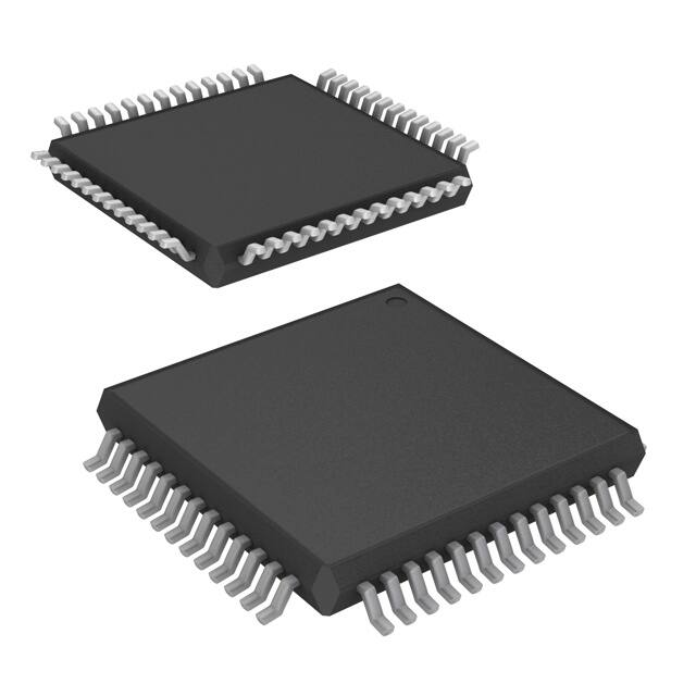


 工商网监
湘ICP备2023018690号
工商网监
湘ICP备2023018690号
