VN772K-E
QUAD SMART POWER SOLID STATE RELAY
FOR COMPLETE H BRIDGE CONFIGURATIONS
Table 1. General Features
Type
VN772K-E
Figure 1. Package
RDS(on)
IOUT
VCC
120mΩ (*)
9A (**)
36V
Note: (*) Total resistance of one side in bridge configuration
Note: (**) Typical current limitation value
SUITED AS LOW VOLTAGE BRIDGE
LINEAR CURRENT LIMITATION
■ VERY LOW STAND-BY POWER DISSIPATION
■ SHORT CIRCUIT PROTECTED
■ DOUBLE STATUS FLAG DIAGNOSTIC (OPEN
DRAIN)
■ INTEGRATED CLAMPING CIRCUITS
■ UNDERVOLTAGE PROTECTION
■
■
■
■
SO-28
ESD PROTECTION
IN COMPLIANCE WITH THE 2002/95/EC
EUROPEAN DIRECTIVE
The high side switches have built-in thermal
shutdown
to
protect
the
chips
from
overtemperature and current limiter blocks to
protect the device from short circuit. Status output
is provided to indicate open load in off and on state
and overtemperature. The low side switches are
two OMNIFET II types (fully autoprotected Power
MOSFET in VIPower™ technology). They have
built-in thermal shutdown, linear current limitation
and overvoltage clamping. Fault feedback for
thermal intervention can be detected by
monitoring the voltage at the input pin.
DESCRIPTION
The VN772K-E is a device formed by three
monolithic chips housed in a standard SO-28
package: a double high side and two low side
switches. Both the double high side and low side
switches are made using |STMicroelectronics
VIPower™ M0-3 Technology. This device is
suitable to drive a DC motor in a bridge
configuration as well as to be used as a quad
switch for any low voltage application.
Table 2. Order Codes
Package
SO-28
Tube
VN772K-E
Tape and Reel
VN772KTR-E
Rev. 1
September 2004
1/21
�VN772K-E
Figure 2. Block Diagram
Vcc
Vcc
CLAMP
OVERVOLTAGE
UNDERVOLTAGE
GND
CLAMP 1
SOURCE1
INPUT1
DRIVER 1
CLAMP 2
DIAG
CURRENT LIMITER 1
LOGIC
DRIVER 2
SOURCE2
OVERTEMP. 1
OPENLOAD ON 1
CURRENT LIMITER 2
INPUT2
OPENLOAD OFF 1
OPENLOAD ON 2
OPENLOAD OFF 2
OVERTEMP. 2
Overvoltage
Clamp
INPUT3
DRAIN3
Gate
Control
SOURCE3
Over
Temperature
Linear
Current
Limiter
Overvoltage
Clamp
INPUT4
DRAIN4
Gate
Control
SOURCE4
Over
Temperature
2/21
Linear
Current
Limiter
�VN772K-E
Table 3. Pin Function
No
1, 3, 25, 28
2
4, 11
5, 10, 19, 24
6
7
8
9
12, 14, 15, 18
13
16, 17
20, 21
22, 23
26, 27
NAME
DRAIN 3
INPUT 3
N.C.
VCC
GND
INPUT 1
DIAGNOSTIC
INPUT 2
DRAIN 4
INPUT 4
SOURCE 4
SOURCE 2
SOURCE 1
SOURCE 3
FUNCTION
Drain of Switch 3 (low-side switch)
Input of Switch 3 (low-side switch)
Not Connected
Drain of Switches 1 and 2 (high-side switches) and Power Supply Voltage
Ground of Switches 1 and 2 (high-side switches)
Input of Switch 1 (high-side switches)
Diagnostic of Switches 1 and 2 (high-side switches)
Input of Switch 2 (high-side switch)
Drain of switch 4 (low-side switch)
Input of Switch 4 (low-side switch)
Source of Switch 4 (low-side switch)
Source of Switch 2 (high-side switch)
Source of Switch 1 (high-side switch)
Source of Switch 3 (low-side switch)
Figure 3. Configuration Diagram (Top View)
Table 4. Thermal Data
Symbol
Rthj-case
Rthj-case
Rthj-amb
Parameter
Thermal Resistance Junction-case (High-side switch)
Thermal Resistance Junction-case (Low-side switch)
Thermal Resistance Junction-ambient
MAX
MAX
MAX
Value
20
20
60
Unit
°C/W
°C/W
°C/W
3/21
�VN772K-E
ABSOLUTE MAXIMUM RATINGS
Table 5. Dual High Side Switch
Symbol
VCC
- VCC
- IGND
IOUT
- IOUT
IIN
ISTAT
VESD
Parameter
DC Supply Voltage
Reverse DC Supply Voltage
DC Reverse Ground Pin Current
DC Output Current
Reverse DC Output Current
DC Input Current
DC Status Current
Electrostatic Discharge (Human Body Model: R=1.5KΩ;
C=100pF)
- INPUT
- STATUS
- OUTPUT
Ptot
Tj
Tc
Tstg
- VCC
Power Dissipation Tc=25°C
Junction Operating Temperature
Case Operating Temperature
Storage Temperature
Value
41
- 0.3
- 200
Internally Limited
-6
+/- 10
+/- 10
Unit
V
V
mA
A
A
mA
mA
4000
V
4000
V
5000
V
5000
V
6
Internally Limited
- 40 to 150
- 55 to 150
W
°C
°C
°C
Table 6. Low Side Switch
Symbol
VDS
VIN
IIN
RIN MIN
ID
IR
VESD1
VESD2
Ptot
Tj
4/21
Parameter
Drain-source Voltage (VIN=0V)
Input Voltage
Input Current
Minimum Input Series Impedance
Drain Current
Reverse DC Output Current
Electrostatic Discharge (R=1.5KΩ, C=100pF)
Electrostatic Discharge on output pin only
(R=330Ω, C=150pF)
Power Dissipation (TC=25°C)
Operating Junction Temperature
Value
Internally Clamped
Internally Clamped
+/-20
150
Internally Limited
-10.5
4000
Unit
V
V
mA
Ω
A
A
V
16500
V
6
Internally limited
W
°C
�VN772K-E
ELECTRICAL CHARACTERISTICS FOR DUAL HIGH SIDE SWITCH
(8V VOL
OVER TEMP STATUS TIMING
Tj > TTSD
VINn
VINn
VSTAT n
VSTAT n
tSDL
tDOL(off)
8/21
tDOL(on)
tSDL
�VN772K-E
Figure 6. Typical Application Diagram
9/21
�VN772K-E
Figure 7. Waveforms
NORMAL OPERATION
INPUTn
OUTPUT VOLTAGEn
STATUSn
UNDERVOLTAGE
VCC
VUSDhyst
VUSD
INPUTn
OUTPUT VOLTAGEn
STATUSn
undefined
OVERVOLTAGE
VCCVOV
VCC
INPUTn
OUTPUT VOLTAGEn
STATUSn
OPEN LOAD with external pull-up
INPUTn
OUTPUT VOLTAGEn
STATUSn
OPEN LOAD without external pull-up
INPUTn
VOUT>VOL
OUTPUT VOLTAGEn
VOL
STATUSn
OVERTEMPERATURE
Tj
TTSD
TR
INPUTn
OUTPUT CURRENTn
STATUSn
10/21
�VN772K-E
Electrical Characterization For Dual High Side Switch
Figure 11. Input Clamp Voltage
Figure 8. Off State Output Current
IL(off1) (uA)
Vicl (V)
2.5
8
2.25
7.8
Off state
Vcc=36V
Vin=Vout=0V
2
1.75
Iin=1mA
7.6
7.4
1.5
7.2
1.25
7
1
6.8
0.75
6.6
0.5
6.4
0.25
6.2
0
6
-50
-25
0
25
50
75
100
125
150
175
-50
-25
0
25
Tc (°C)
50
75
100
125
150
175
100
125
150
175
150
175
Tc (°C)
Figure 12. Input High Level
Figure 9. High Level Input Current
Iih (uA)
Vih (V)
5
3.6
4.5
3.4
Vin=3.25V
4
3.2
3.5
3
3
2.5
2.8
2
2.6
1.5
2.4
1
2.2
0.5
0
2
-50
-25
0
25
50
75
100
125
150
175
-50
-25
0
25
Tc (°C)
50
75
Tc (°C)
Figure 10. Input Low Level
Figure 13. Input Hysteresis Voltage
Vil (V)
Vhyst (V)
2.6
1.5
1.4
2.4
1.3
2.2
1.2
2
1.1
1.8
1
0.9
1.6
0.8
1.4
0.7
1.2
0.6
1
0.5
-50
-25
0
25
50
75
Tc (°C)
100
125
150
175
-50
-25
0
25
50
75
100
125
Tc (°C)
11/21
�VN772K-E
Electrical Characterization For Dual High Side Switch (continued)
Figure 14. Overvoltage Shutdown
Figure 17. ILIM Vs Tcase
Vov (V)
Ilim (A)
50
20
48
18
46
16
44
14
42
12
40
10
38
8
36
6
34
4
32
2
Vcc=13V
30
0
-50
-25
0
25
50
75
100
125
150
175
-50
-25
0
25
Tc (°C)
100
125
150
175
150
175
Figure 18. Turn-off Voltage Slope
dVout/dt(on) (V/ms)
dVout/dt(off) (V/ms)
800
600
550
Vcc=13V
Rl=6.5Ohm
600
75
Tc (°C)
Figure 15. Turn-on Voltage Slope
700
50
Vcc=13V
Rl=6.5Ohm
500
500
450
400
400
300
350
200
300
100
250
0
200
-50
-25
0
25
50
75
100
125
150
175
-50
-25
0
25
Tc (ºC)
50
75
Figure 16. On State Resistance Vs Tcase
Ron (mOhm)
160
120
Tc=150°C
110
Iout=2A
Vcc=8V; 13V & 36V
120
125
Figure 19. On State Resistance Vs VCC
Ron (mOhm)
140
100
Tc (ºC)
100
90
80
100
70
60
80
Tc=25°C
50
60
40
Tc= - 40°C
30
40
20
Iout=5A
20
10
0
0
-50
-25
0
25
50
75
Tc (°C)
12/21
100
125
150
175
5
10
15
20
25
Vcc (V)
30
35
40
�VN772K-E
Electrical Characterization For Dual High Side Switch (continued)
Figure 23. Status Low Output Voltage
Figure 20. Status Leakage Current
Ilstat (uA)
Vstat (V)
0.05
0.8
0.7
Istat=1.6mA
0.04
0.6
Vstat=5V
0.5
0.03
0.4
0.02
0.3
0.2
0.01
0.1
0
0
-50
-25
0
25
50
75
100
125
150
175
-50
-25
0
25
Tc (°C)
50
75
100
125
150
175
Tc (°C)
Figure 24. Openload Off State Voltage
Detection Threshold
Figure 21. Openload On State Detection
Threshold
Iol (mA)
Vol (V)
150
5
140
4.5
Vin=0V
Vcc=13V
Vin=5V
130
4
120
3.5
110
3
100
2.5
90
2
80
1.5
70
1
60
0.5
50
0
-50
-25
0
25
50
75
100
125
150
175
Tc (ºC)
-50
-25
0
25
50
75
100
125
150
175
Tc (°C)
Figure 22. Status Clamp Voltage
Vscl (V)
8
7.8
Istat=1mA
7.6
7.4
7.2
7
6.8
6.6
6.4
6.2
6
-50
-25
0
25
50
75
100
125
150
175
Tc (°C)
13/21
�VN772K-E
Electrical Characterization For Low Side Switches
Figure 25. Static Drain Source On Resistance
Figure 28. Derating Curve
Rds(on) (mOhm)
500
Tj= - 40ºC
450
Vin=2.5V
400
350
Tj=25ºC
300
250
Tj=150ºC
200
150
100
50
0
0
0.25
0.5
0.75
1
1.25
Id(A)
Figure 26. Transconductance
Figure 29. Transfer Characteristics
Gfs (S)
Idon(A)
20
10
18
Tj=25ºC
9
Vds=13V
Tj=-40ºC
Vds=13.5V
16
Tj=-40ºC
Tj=25ºC
14
Tj=150ºC
8
7
Tj=150ºC
12
6
10
5
8
4
6
3
4
2
2
1
0
0
0
1
2
3
4
5
6
7
8
1
1.5
2
2.5
3
Id(A)
Figure 27. Turn On Current Slope
4
4.5
5
Figure 30. Turn On Current Slope
di/dt(A/us)
di/dt(A/us)
8
2.25
7
2
Vin=5V
Vdd=15V
Id=3.5A
6
1.5
4
1.25
3
1
2
0.75
1
0.5
0
Vin=3.5V
Vdd=15V
Id=3.5A
1.75
5
0.25
100
200
300
400
500
600
Rg(ohm)
14/21
3.5
Vin(V)
700
800
900 1000 1100
100
200
300
400
500
600
700
Rg(ohm)
800
900 1000 1100
5.5
�VN772K-E
Electrical Characterization For Low Side Switches (continued)
Figure 31. Input Voltage Vs. Input Charge
Figure 34. Capacitance Variations
C(pF)
Vin(V)
600
8
7
Vds=12V
Id=3.5A
6
500
f=1MHz
Vin=0V
5
400
4
300
3
2
200
1
100
0
0
5
10
15
20
0
25
5
10
15
20
25
30
35
Vds(V)
Qg(nC)
Figure 32. Switching Time Resistive Load
t(us)
Figure 35. Switching Time Resistive Load
t(ns)
5.5
1600
tr
5
Vdd=15V
Id=3.5A
Vin=5V
4.5
4
1400
tr
td(off)
Vdd=15V
Id=3.5A
Rg=150ohm
1200
tf
3.5
1000
3
800
2.5
2
600
1.5
td(off)
400
1
tf
td(on)
0.5
200
0
td(on)
0
250
500
0
750 1000 1250 1500 1750 2000 2250 2500
3.25
3.5
3.75
4
Rg(ohm)
4.25
4.5
4.75
5
5.25
Vin(V)
Figure 33. Output Characteristics
Figure 36. Step Response Current Limit
ID(A)
Tdlim(us)
12
7
11
6.5
10
9
Vin=5V
Vin=4.5V
8
Vin=4V
Vin=5V
Rg=150ohm
6
7
5.5
Vin=3V
6
5
5
4
4.5
3
Vin=2.5V
2
4
1
Vin=2V
0
3.5
0
1
2
3
4
5
6
7
VDS(V)
8
9
10
11
12
13
5
10
15
20
25
30
35
Vdd(V)
15/21
�VN772K-E
Electrical Characterization For Low Side Switches (continued)
Figure 37. Source-Drain Diode Forward
Characteristics
Figure 40. Static Drain-Source On Resistance
Vs. Id
Vsd (mV)
Rds(on) (mOhm)
1000
140
950
120
Vin=0V
900
Vin=3.5V
100
850
Tj=150ºC
Vin=5V
800
80
750
60
700
Vin=3.5V
Tj=25ºC
650
Vin=5V
Vin=3.5V
40
Tj=-40ºC
600
Vin=5V
20
550
500
0
0
2
4
6
8
10
12
14
0
0.5
1
1.5
2
Id(A)
2.5
3
3.5
4
4.5
5
5.5
6
Id(A)
Figure 38. Static Drain-Source On resistance
Vs. Input Voltage
Figure 41. Static Drain-Source On resistance
Vs. Input Voltage
Rds(on) (mOhm)
Rds(on) (mOhm)
140
120
110
120
Id=3.5A
100
Tj=150ºC
90
100
Tj=150ºC
80
Id=6A
Id=1A
80
70
60
60
Tj=25ºC
50
Tj=25ºC
40
Tj=-40ºC
20
Id=6A
40
Id=1A
30
Id=6A
Id=1A
20
Tj= - 40ºC
10
0
0
3
3.5
4
4.5
5
5.5
6
6.5
3
3.5
4
4.5
Vin(V)
5
5.5
6
6.5
7
Vin(V)
Figure 39. Normalized Input Threshold Voltage
Vs. Temperature
Figure 42. Normalized On Resistance Vs.
Temperature
Vin(th)
Rds(on)
1.15
2.25
1.1
2
Vds=Vin
Id=1mA
1.05
Vin=5V
Id=3.5A
1.75
1
0.95
1.5
0.9
1.25
0.85
1
0.8
0.75
0.75
0.5
0.7
-50
-25
0
25
50
75
T(ºC)
16/21
100
125
150
175
-50
-25
0
25
50
75
T(ºC)
100
125
150
175
�VN772K-E
Electrical Characterization For Low Side Switches (continued)
Figure 43. Turn off drain source voltage slope
Figure 45. Turn off drain source voltage slope
dv/dt(V/us)
dv/dt(v/us)
300
300
250
250
Vin=3.5V
Vdd=15V
Id=3.5A
200
Vin=5V
Vdd=15V
Id=3.5A
200
150
150
100
100
50
50
0
0
100
200
300
400
600
500
700
800
900 1000 1100
100
200
300
400
500
600
700
800
900 1000 1100
Rg(ohm)
Rg(ohm)
Figure 44. Current Limit Vs. Junction
Temperature
Ilim (A)
15
14
Vds=13V
Vin=5V
13
12
11
10
9
8
7
6
5
-50
-25
0
25
50
75
100
125
150
175
Tj (ºC)
17/21
�VN772K-E
Table 20. SO-28 Mechanical Data
Symbol
A
a1
b
b1
C
c1
D
E
e
e3
F
L
S
millimeters
Min
Max
2.65
0.30
0.49
0.32
0.10
0.35
0.23
0.50
45° (typ.)
17.7
10.00
18.1
10.65
1.27
16.51
7.40
0.40
Figure 46. SO-28 Package Dimensions
18/21
Typ
7.60
1.27
8° (max.)
�VN772K-E
Figure 47. SO-28 Tube Shipment (No Suffix)
Base Q.ty
Bulk Q.ty
Tube length (± 0.5)
A
B
C (± 0.1)
C
B
28
700
532
3.5
13.8
0.6
All dimensions are in mm.
A
Figure 48. Tape And Reel Shipment (Suffix “TR”)
REEL DIMENSIONS
Base Q.ty
Bulk Q.ty
A (max)
B (min)
C (± 0.2)
F
G (+ 2 / -0)
N (min)
T (max)
1000
1000
330
1.5
13
20.2
16.4
60
22.4
TAPE DIMENSIONS
According to Electronic Industries Association
(EIA) Standard 481 rev. A, Feb. 1986
Tape width
Tape Hole Spacing
Component Spacing
Hole Diameter
Hole Diameter
Hole Position
Compartment Depth
Hole Spacing
W
P0 (± 0.1)
P
D (± 0.1/-0)
D1 (min)
F (± 0.05)
K (max)
P1 (± 0.1)
16
4
12
1.5
1.5
7.5
6.5
2
End
All dimensions are in mm.
Start
Top
No components
Components
No components
cover
tape
500mm min
Empty components pockets
saled with cover tape.
500mm min
User direction of feed
19/21
�VN772K-E
REVISION HISTORY
Date
Sep. 2004
20/21
Revision
1
- First Issue.
Description of Changes
�VN772K-E
Information furnished is believed to be accurate and reliable. However, STMicroelectronics assumes no responsibility for the consequences
of use of such information nor for any infringement of patents or other rights of third parties which may result from its use. No license is granted
by implication or otherwise under any patent or patent rights of STMicroelectronics. Specifications mentioned in this publication are subject
to change without notice. This publication supersedes and replaces all information previously supplied. STMicroelectronics products are not
authorized for use as critical components in life support devices or systems without express written approval of STMicroelectronics.
The ST logo is a registered trademark of STMicroelectronics.
All other names are the property of their respective owners
© 2004 STMicroelectronics - All rights reserved
STMicroelectronics group of companies
Australia - Belgium - Brazil - Canada - China - Czech Republic - Finland - France - Germany - Hong Kong - India - Israel - Italy - Japan Malaysia - Malta - Morocco - Singapore - Spain - Sweden - Switzerland - United Kingdom - United States of America
www.st.com
21/21
�
很抱歉,暂时无法提供与“VN772KTR-E”相匹配的价格&库存,您可以联系我们找货
免费人工找货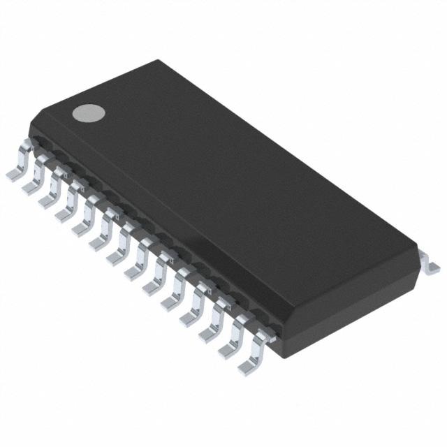


 工商网监
湘ICP备2023018690号
工商网监
湘ICP备2023018690号
