VND830ASP
®
DOUBLE CHANNEL HIGH SIDE SOLID STATE RELAY
TYPE
VND830ASP
RDS(on)
60 mΩ (*)
IOUT
6 A (*)
VCC
36 V (*)
(*) Per channel
)
s
(
ct
10
DC SHORT CIRCUIT CURRENT: 6A
■ CMOS COMPATIBLE INPUTS
■ PROPORTIONAL LOAD CURRENT SENSE
■ UNDERVOLTAGE AND OVERVOLTAGE
SHUT-DOWN
■ OVERVOLTAGE CLAMP
■ THERMAL SHUT-DOWN
■ CURRENT LIMITATION
■ VERY LOW STAND-BY POWER DISSIPATION
■
PROTECTION AGAINST:
LOSS OF GROUND AND LOSS OF VCC
■ REVERSE BATTERY PROTECTION (**)
■
)
(s
DESCRIPTION
The VND830ASP is a monolithic device made using
STMicroelectronics VIPower M0-3 technology. It
is intended for driving any kind of load with one
t
c
u
BLOCK DIAGRAM
d
o
r
1
PowerSO-10™
s
b
O
Pr
PACKAGE
TUBE
T&R
PowerSO-10™ VND830ASP VND830ASP13TR
e
t
e
ol
side connected to ground. Active VCC pin voltage
clamp protects the device against low energy
spikes (see ISO7637 transient compatibility table).
This device has two channels in high side
configuration; each channel has an analog sense
output on which the sensing current is proportional
(according to a known ratio) to the corresponding
load current. Built-in thermal shut-down and
outputs current limitation protect the chip from
over temperature and short circuit. Device turns off
in case of ground pin disconnection.
s
b
O
P
e
t
e
l
o
u
d
o
ORDER CODES
VCC
OVERVOLTAGE
VCC CLAMP
UNDERVOLTAGE
PwCLAMP 1
DRIVER 1
OUTPUT 1
ILIM1
INPUT 1
Vdslim1
LOGIC
IOUT1
INPUT 2
Ot1
CURRENT
SENSE 1
K
PwCLAMP 2
DRIVER 2
GND
Ot1
OVERTEMP. 1
OVERTEMP. 2
Vdslim2
Ot2
OUTPUT 2
ILIM2
IOUT2
K
Ot2
CURRENT
SENSE 2
(**) See application schematic at page 8
September 2013
DocID9696 Rev 3
1/17
�VND830ASP
ABSOLUTE MAXIMUM RATING
Symbol
VCC
-VCC
-IGND
IOUT
IR
IIN
VCSENSE
Parameter
DC Supply Voltage
Reverse Supply Voltage
DC Reverse Ground Pin Current
Output Current
Reverse Output Current
Input Current
Current Sense Maximum Voltage
Value
41
- 0.3
- 200
Internally Limited
-6
+/- 10
-3
Unit
V
V
mA
A
A
mA
V
+15
V
)
s
(
ct
Electrostatic Discharge (Human Body Model: R=1.5Ω; C=100pF)
VESD
- INPUT
4000
- CURRENT SENSE
2000
u
d
o
- OUTPUT
EMAX
Ptot
Tj
Tc
Tstg
5000
- VCC
Maximum Switching Energy
(L=1.8mH; RL=0Ω; Vbat=13.5V; Tjstart=150ºC; IL=9A)
Power Dissipation at TC=25°C
Junction Operating Temperature
Case Operating Temperature
Storage Temperature
o
s
b
O
)
CONNECTION DIAGRAM (TOP VIEW)
GROUND
INPUT2
INPUT1
C.SENSE1
C.SENSE2
s
(
t
c
u
d
o
e
t
e
ol
Pr
OUTPUT 2
OUTPUT 2
N.C.
OUTPUT 1
OUTPUT 1
5
4
3
6
7
8
9
2
10
1
11
VCC
CURRENT AND VOLTAGE CONVENTIONS
s
b
O
IS
VCC
IIN1
INPUT1
VIN1
OUTPUT1
VIN2
IOUT2
INPUT2
VOUT1
ISENSE1
CURRENT SENSE 1
IIN2
OUTPUT2
CURRENT SENSE 2
GROUND
IGND
2/17
VCC
IOUT1
VSENSE1
VOUT2
ISENSE2
VSENSE2
V
V
5000
V
100
mJ
74
Internally Limited
- 40 to 150
- 55 to 150
W
°C
°C
°C
r
P
e
let
V
�VND830ASP
THERMAL DATA
Symbol
Rthj-case
Parameter
Thermal Resistance Junction-case
Value
1.2
Unit
°C/W
Rthj-amb
Thermal Resistance Junction-ambient
51.2 (*)
°C/W
(*) When mounted on a standard single-sided FR-4 board with 0.5cm2 of Cu (at least 35µm thick). Horizontal mounting and no artificial air
flow
ELECTRICAL CHARACTERISTICS (8V
很抱歉,暂时无法提供与“VND830ASP”相匹配的价格&库存,您可以联系我们找货
免费人工找货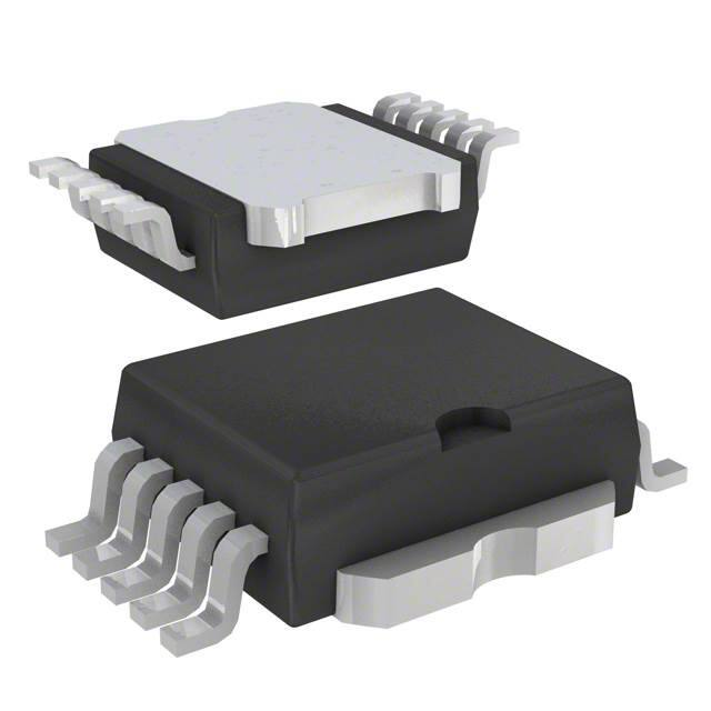


 工商网监
湘ICP备2023018690号
工商网监
湘ICP备2023018690号
