Z04
Standard
4 A Triacs
Main features
A2
Symbol
Value
Unit
IT(RMS)
4
A
VDRM/VRRM
600 to 800
V
IGT (Q1)
3 to 25
mA
G
A1
Description
A1
A2
The Z04 series is suitable for general purpose AC
switching applications. They can be found in
applications such as home appliances
(electrovalve, pump, door lock, small lamp
control), fan speed controllers,...
G
TO202-3
Different gate current sensitivities are available,
allowing optimized performances when controlled
directly from microcontrollers.
Order codes
Part Number
Marking
Z04xxyF(1)
Z04xxyF(1)
1. xx = sensitivity, y = voltage
Table 1.
Absolute maximum ratings
Symbol
IT(RMS)
ITSM
I ²t
Parameter
Tamb = 25° C
RMS on-state current (full sine wave)
Value
Unit
4
A
Tl = 30° C
Non repetitive surge peak on-state current
(full cycle, Tj initial = 25° C)
F = 50 Hz
t = 20 ms
20
F = 60 Hz
t = 16.7 ms
21
I²t Value for fusing
tp = 10 ms
A
2.2
A ²s
dI/dt
Critical rate of rise of on-state current IG =
F = 120 Hz
2 x IGT , tr ≤ 100 ns
Tj = 125° C
20
A/µs
IGM
Peak gate current
Tj = 125° C
1.2
A
Tj = 125° C
0.2
W
- 40 to + 150
- 40 to + 125
°C
PG(AV)
Tstg
Tj
May 2006
tp = 20 µs
Average gate power dissipation
Storage junction temperature range
Operating junction temperature range
Rev 7
1/8
www.st.com
8
�Characteristics
1
Z04
Characteristics
Table 2.
Electrical Characteristics (Tj = 25° C, unless otherwise specified)
Z04
Symbol
Test Conditions
Quadrant
IGT (1)
VGD
VD = VDRM RL = 3.3 kΩ
Tj = 125° C
IH (2)
IT = 50 mA
IL
IG = 1.2 IGT
(dV/dt)c
(2)
09
10
3
5
10
25
MAX
.
ALL
MAX
.
1.3
V
ALL
MIN.
0.2
V
MAX
.
I - III - IV
dV/dt (2)
05
I - II - III - IV
VD = 12 V RL = 30 Ω
VGT
Unit
02
3
5
10
25
mA
mA
MAX
.
6
10
15
25
12
15
25
50
VD = 6 % VDRM gate open Tj = 110° C
MIN.
10
20
100
200
V/µs
(dI/dt)c = 1.8 A/ms
MIN.
0.5
1
2
5
V/µs
II
Tj = 110° C
mA
1. minimum IGT is guaranted at 5% of IGT max.
2. for both polarities of A2 referenced to A1.
Table 3.
Static Characteristics
Symbol
Test Conditions
VTM (1)
ITM = 5.5 A
Vto (1)
Rd
(1)
IDRM
IRRM
tp = 380 µs
Value
Unit
Tj = 25° C
MAX.
2.0
V
Threshold voltage
Tj = 125° C
MAX.
0.95
V
Dynamic resistance
Tj = 125° C
MAX.
180
mΩ
5
µA
0.5
mA
VDRM = VRRM
Tj = 25° C
Tj = 125° C
MAX.
1. for both polarities of A2 referenced to A1.
Table 4.
Thermal resistances
Symbol
2/8
Parameter
Value
Unit
Rth(j-I)
Junction to lead (AC)
15
° C/W
Rth(j-a)
Junction to ambient
100
° C/W
�Z04
Characteristics
Figure 1.
Maximum power dissipation
versus RMS on-state current
(full cycle)
Figure 2.
P(W)
RMS on-state current versus
ambient temperature (full cycle)
IT(RMS)(A)
7
4.5
Rth(j-a) = Rth(j-l)
4.0
6
3.5
5
3.0
4
2.5
3
2.0
1.5
Rth(j-a) = 100°C/W
2
1.0
1
0.5
IT(RMS)(A)
Tamb (°C)
0.0
0
0.0
0.5
1.0
Figure 3.
1.5
2.0
2.5
3.0
3.5
0
4.0
Relative variation of thermal
impedance versus pulse
duration
25
Figure 4.
50
75
100
125
Relative variation of gate trigger
current, holding current and
latching current versus junction
temperature (typical values)
IGT, IH, IL [Tj] / IGT, IH, IL [Tj=25°C]
K=[Zth(j-a)/Rth(j-a)]
2.5
1E+0
2.0
1E-1
1.5
IGT
IH & IL
1.0
1E-2
0.5
Tj (°C)
tp(s)
1E-3
0.0
1E-3
1E-2
Figure 5.
1E-1
1E+0
1E+1
1E+2
5E+2
Surge peak on-state current
versus number of cycles
-40
-20
Figure 6.
0
20
40
60
80
100
120
140
Non-repetitive surge peak on-state
current for a sinusoidal pulse with
width tp < 10 ms and corresponding
value of I2t
ITSM (A), I2t (A2s)
ITSM (A)
25
500
Tj initial = 25°C
t=20ms
20
100
One cycle
dI/dt limitation:
20A/µs
15
ITSM
Non repetitive
Tj initial = 25°C
10
Repetitive
Tamb = 25°C
10
5
I2t
tp (ms)
Number of cycles
0
1
10
100
1000
1
0.01
0.10
1.00
10.00
3/8
�Characteristics
Figure 7.
Z04
On-state characteristics
(maximum values)
Figure 8.
ITM(A)
(dI/dt)c [(dV/dt)c] / Specified (dI/dt)c
20.0
2.6
2.4
2.2
2.0
1.8
1.6
1.4
1.2
1.0
0.8
0.6
0.4
0.2
0.0
10.0
Tj = Tjmax.
1.0
Tj = 25°C
Tj=max.
Vt0=0.95 V
Rd=180 mΩ
VTM (V)
0.1
0.0
Figure 9.
0.5
1.0
1.5
2.0
2.5
3.0
3.5
4.0
4.5
5.0
Relative variation of critical
rate of decrease of main current
versus junction temperature
(dI/dt)c [Tj] / (dI/dt)c [Tj Specified]
6
5
4
3
2
1
Tj (°C)
0
4/8
0
Relative variation of critical rate of
decrease of main current versus
(dV/dt)c (typical values)
25
50
75
100
125
Z0410
Z0409
Z0402
Z0405
(dV/dt)c (V/µs)
0.1
1.0
10.0
100.0
�Z04
2
Ordering information scheme
Ordering information scheme
Z 04 xx y F
[BLANK]
0AA2
Triac series
Current
04 = 4A
Sensitivity
02 = 3mA
05 = 5mA
09 = 10mA
10 = 25mA
Voltage
M = 600V
S = 700V
N = 800V
Package
F = TO202-3
Packing mode
0AA2 = Tube
Table 5.
Product selector
Voltage
Part Number
Sensitivity
Type
Package
Standard
TO202-3
600 V 700 V 800 V
Z0402MF
X
Z0402SF
3 mA
X
Z0402NF
Z0405MF
X
X
Z0405SF
X
X
Z0410SF
Z0410NF
5 mA
10 mA
X
Z0409NF
Z0410MF
5 mA
X
Z0409SF
3 mA
5 mA
Z0405NF
Z0409MF
3 mA
10 mA
X
X
10 mA
25 mA
X
25 mA
X
25 mA
5/8
�Package information
3
Z04
Package information
DIMENSIONS
REF.
Millimeters
Min.
Typ.
A
A
C
F
D
J
P
H
N1
N
Typ.
7.3
0.287
D
10.5
0.413
1.5
0.059
H
0.51
0.020
J
1.5
0.059
M
4.5
0.177
N1
5.3
2.54
Max.
0.398
C
N
M
Min.
10.1
F
O
Max.
Inches
0.209
0.100
O
1.4
0.055
P
0.7
0.028
In order to meet environmental requirements, ST offers these devices in ECOPACK®
packages. These packages have a lead-free second level interconnect. The category of
second level interconnect is marked on the package and on the inner box label, in
compliance with JEDEC Standard JESD97. The maximum ratings related to soldering
conditions are also marked on the inner box label. ECOPACK is an ST trademark.
ECOPACK specifications are available at: www.st.com.
6/8
�Z04
4
Ordering information
Ordering information
Ordering type
Marking
Weight
Base qty
Delivery mode
Z04xxyF 0AA2(1)
Z04xxyF(1)
0.8 g
50
Tube
1. xx = sensitivity, y = voltage
5
Revision history
Date
Revision
Description of Changes
Oct-2001
4
Last update.
13-Feb-2006
5
TO202-3 delivery mode changed from bulk to tube.
ECOPACK statement added.
31-Mar-2006
6
Reformatted to current standard. Lead marking changed
on page 1
12-05-2006
7
Typographical error for (dV/dt)c corrected in Table 2.
7/8
�Z04
Please Read Carefully:
Information in this document is provided solely in connection with ST products. STMicroelectronics NV and its subsidiaries (“ST”) reserve the
right to make changes, corrections, modifications or improvements, to this document, and the products and services described herein at any
time, without notice.
All ST products are sold pursuant to ST’s terms and conditions of sale.
Purchasers are solely responsible for the choice, selection and use of the ST products and services described herein, and ST assumes no
liability whatsoever relating to the choice, selection or use of the ST products and services described herein.
No license, express or implied, by estoppel or otherwise, to any intellectual property rights is granted under this document. If any part of this
document refers to any third party products or services it shall not be deemed a license grant by ST for the use of such third party products
or services, or any intellectual property contained therein or considered as a warranty covering the use in any manner whatsoever of such
third party products or services or any intellectual property contained therein.
UNLESS OTHERWISE SET FORTH IN ST’S TERMS AND CONDITIONS OF SALE ST DISCLAIMS ANY EXPRESS OR IMPLIED
WARRANTY WITH RESPECT TO THE USE AND/OR SALE OF ST PRODUCTS INCLUDING WITHOUT LIMITATION IMPLIED
WARRANTIES OF MERCHANTABILITY, FITNESS FOR A PARTICULAR PURPOSE (AND THEIR EQUIVALENTS UNDER THE LAWS
OF ANY JURISDICTION), OR INFRINGEMENT OF ANY PATENT, COPYRIGHT OR OTHER INTELLECTUAL PROPERTY RIGHT.
UNLESS EXPRESSLY APPROVED IN WRITING BY AN AUTHORIZE REPRESENTATIVE OF ST, ST PRODUCTS ARE NOT DESIGNED,
AUTHORIZED OR WARRANTED FOR USE IN MILITARY, AIR CRAFT, SPACE, LIFE SAVING, OR LIFE SUSTAINING APPLICATIONS,
NOR IN PRODUCTS OR SYSTEMS, WHERE FAILURE OR MALFUNCTION MAY RESULT IN PERSONAL INJURY, DEATH, OR
SEVERE PROPERTY OR ENVIRONMENTAL DAMAGE.
Resale of ST products with provisions different from the statements and/or technical features set forth in this document shall immediately void
any warranty granted by ST for the ST product or service described herein and shall not create or extend in any manner whatsoever, any
liability of ST.
ST and the ST logo are trademarks or registered trademarks of ST in various countries.
Information in this document supersedes and replaces all information previously supplied.
The ST logo is a registered trademark of STMicroelectronics. All other names are the property of their respective owners.
© 2006 STMicroelectronics - All rights reserved
STMicroelectronics group of companies
Australia - Belgium - Brazil - Canada - China - Czech Republic - Finland - France - Germany - Hong Kong - India - Israel - Italy - Japan Malaysia - Malta - Morocco - Singapore - Spain - Sweden - Switzerland - United Kingdom - United States of America
www.st.com
8/8
�
很抱歉,暂时无法提供与“Z0405MF0AA2”相匹配的价格&库存,您可以联系我们找货
免费人工找货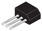


 工商网监
湘ICP备2023018690号
工商网监
湘ICP备2023018690号
