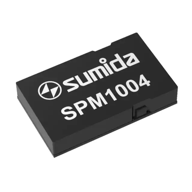
SPM1004
12V Input 6A Output Power Supply in Inductor (PSI2) Module
FEATURES
DESCRIPTION
SPM1004 is an easy-to-use 6A output integrated Point of
Load (POL) power supply module. It contains integrated
power MOSFETs, driver, PWM controller, a high
performance inductor, input and output capacitors and
other passive components in one low profile LGA package
using PSI2 technology.
Only one external input capacitor and one external output
capacitor are needed for typical applications. There is no
need for loop compensation, sensitive PCB layout,
inductor selection, or in-circuit production testing. Each
module is fully tested.
SPM1004 integrated POL power module series are offered
with eight models for eight different output voltages:
5.0V, 3.3V, 2.5V, 1.8V, 1.5V, 1.2V, 1.0V, and 0.8V. Each
output voltage can be trimmed by ±10%.
All SPM1004 models deliver full 6A load current without
derating at 85°C ambient temperature with no airflow.
Small size (15mm x 9mm) and low profile (2.8mm) allows
SPM1004 to be placed very close to its load or on the back
side of the PCB for high density applications.
Constant-on-time (COT) control is used to achieve
excellent transient response to line and load changes
without sacrificing stability and high efficiency at light
load.
Sumida's PSI2 technology ensures optimal inductor design,
uniform temperature distribution and very low
temperature difference between case and IC die.
Integrated Point of Load power module using PSI2
Power Supply in Inductor technology
Small footprint, low-profile, 15mm x 9mm x
2.8mm, with LGA Package (with 0.63 mm pads)
Efficiency of 95.2% at 3A and 94.2% at 6A for 5V
output
High output current, 6A without derating at 85°C
ambient with no air flow
Wide output voltage selections: from 0.8V to 5V
output voltages with ±10% trim capability
Output voltage remote sensing
Pre-bias startup capability
Adjustable soft-start time
Enable signal input and Power Good signal output
Output voltage sequencing
Programmable Under Voltage Lock Out (UVLO)
Output Over-Current Protection (OCP)
Over-temperature protection
Operating temperature range -40°C to 85°C
Excellent thermal performance
MSL 3 and RoHS compliant
APPLICATIONS
Broadband and communications equipment
DSP and FPGA Point of Load applications
High density distributed power systems
Systems using PCI / PCI express / PXI express
Automated test and medical equipment
SIMPLIFIED APPLICATION
EFFICIENCY VS LOAD CURRENT (VIN = 12V)
97
PWRGD
SS
96
VSENSE
VOUT
VIN
PVIN
VOUT
SPM1004
CIN
EN
VADJ
AGND
PGND
COUT
Efficiency (%)
VAUX
PHASE
95
94
93
92
Vout = 5.0 V
91
Vout = 3.3 V
90
0
Version 3.0
July 29, 2015
1
2
3
4
Output Current (A)
5
6
Page 1 of 28
�SPM1004
ABSOLUTE MAXIMUM(1) RATINGS over operating temperature range (unless
otherwise noted)
VALUE
Unit
MAX
PVIN
18
V
EN
6
V
Input Signals
VSENSE
6
V
VADJ
6
V
SS
6
V
VOUT
PVIN
V
PHASE
PVIN
V
Output Signals
PWRGD
6
V
VAUX
6
V
Current
EN
2.5
mA
Operating Junction Temperature
-40
150
°C
Temperature
Storage Temperature
-65
150
°C
Lead Temperature (soldering)
260
°C
(1) Stresses beyond those listed under absolute maximum ratings may cause permanent damage to the module. These are stress
ratings only, and functional operation of the module at these or any other conditions beyond those indicated under
recommended operating conditions is not implied. Exposure to absolute-maximum-rated conditions for extended periods may
affect reliability.
MIN
-0.3
-0.3
-0.3
-0.3
-0.3
-0.6
-0.6
-0.3
-0.3
Version 3.0
July 29, 2015
Page 2 of 28
�SPM1004
ELECTRICAL CHARACTERISTICS
The electrical characteristics are presented in two parts. Part 1 provides the electrical characteristics that are common
to all models and Part 2 provides the electrical characteristics that are specific to each model.
The electrical performance is based on the following conditions unless otherwise stated: over the full range from -40°C
to 85°C ambient temperature, no air flow; VIN = 12V, IOUT = 6A, CIN = 100μF ceramic, COUT = 200μF ceramic.
Part 1: Electrical Characteristics Common to All Models:
IOUT:
VIN:
VEN_ON
VEN_OFF
PARAMETERS
Output current
Input voltage
Enable on voltage
Enable off voltage
IEN
Enable input current
ISTBY
Input standby current
PWRGD Power Good Signal
OVP
Over-Voltage Protection
Thermal shutdown (die temperature)
VAUX: Auxiliary output
CVAUX: External capacitor at VAUX
CPVIN: External capacitor at PVIN
COUT: External output capacitor
Version 3.0
TEST CONDITIONS
TA = -40°C to 85°C, natural convection
TA = -40°C to 85°C; IOUT 0 to max
Enable high voltage (module turned on)
Enable low voltage (module turned off)
VEN = 2V
VEN = 0V
EN pin to PGND (shut down), TA = 25°C
EN = 2V, IOUT = 0A, TA = 25°C
PWRGD high
VOUT rising
Leakage current
(% of VOUT)
PWRGD delay
PWRGD low
VOUT falling
(% of VOUT)
At 4mA sink current
OVP threshold (percentage of nominal)
OVP shutdown delay
Thermal shutdown
Thermal shutdown recovery hysteresis
Output voltage
Output current
Ceramic
Ceramic
Non-ceramic
Ceramic
Non-ceramic (Electrolytic or tantalum)
July 29, 2015
MIN
0
9
1.1
87%
117%
4.6
TYP
12
1.3
0.5
0.1
0
0.2
1.0
91%
10
2.5
80%
120%
2
170
15
4.8
MAX
6
15
0.6
0.5
2.5
94%
100
0.4
123%
5.0
1
22
47
100
220
200
500
2000
UNIT
A
V
V
V
mA
μA
mA
mA
nA
ms
V
V
μs
°C
°C
V
mA
μF
μF
μF
μF
μF
Page 3 of 28
�SPM1004
Part 2: Electrical Characteristics Specific for Each Individual Model
SPM1004-5V0
PARAMETERS
VSTART Startup voltage
UVLO Under Voltage Lock Out
VOUT(adj): Output voltage trim range
Set point accuracy
Temperature variation
VOUT
Line regulation
Load regulation
Total variation
Vo_rip, Output voltage ripple
η
Efficiency
Transient Response
FS
ILIM
Switching frequency
Current Limit Point
TEST CONDITIONS
Over IOUT range
Over IOUT range
Over IOUT range
TA = 25°C, VIN = 12V, IOUT = 3A
-40°C < TA < +85°C, IOUT = 3A
Over VIN range, TA = 25°C, IOUT = 3A
Over IOUT range, TA = 25°C, VIN = 12V
Set-point, line, load, temperature variation
20MHz bandwidth, VIN = 12V, IOUT = 6A
IOUT = 3A
VIN = 12V
IOUT = 6A
IOUT = 3A
VIN = 9V
IOUT = 6A
IOUT = 3A
VIN = 15V
IOUT = 6A
Over/undershoot
1A/μs load step
between 2A and 5A
Recovery time
VIN = 12V, IOUT = 6A
VIN = 12V, TA = 25°C
MIN
8.5
7.0
4.5
TEST CONDITIONS
Over IOUT range
Over IOUT range
Over IOUT range
TA = 25°C, VIN = 12V, IOUT = 3A
-40°C < TA < +85°C, IOUT = 3A
Over VIN range, TA = 25°C, IOUT = 3A
Over IOUT range, TA = 25°C, VIN = 12V
Set-point, line, load, temperature variation
20MHz bandwidth, VIN = 12V, IOUT = 6A
IOUT = 3A
VIN = 12V
IOUT = 6A
IOUT = 3A
VIN = 9V
IOUT = 6A
IOUT = 3A
VIN = 15V
IOUT = 6A
Over/undershoot
1A/μs load step
between 2A and 5A
Recovery time
VIN = 12V, IOUT = 6A
VIN = 12V, TA = 25°C
MIN
8.0
6.5
2.97
TYP
9.0
7.5
5.0
±1%
±0.5%
±0.5%
±1%
MAX
9.5
8.0
5.5
UNIT
V
V
V
±4%
20
95.2%
94.2%
96.1%
94.5%
94.3%
93.7%
30
75
800
8.5
mVpp
mV
μs
kHz
A
SPM1004-3V3
PARAMETERS
VSTART Startup voltage
UVLO Under Voltage Lock Out
VOUT(adj): Output voltage trim range
Set point accuracy
Temperature variation
VOUT
Line regulation
Load regulation
Total variation
Vo_rip, Output voltage ripple
η
Efficiency
Transient Response
FS
ILIM
Switching frequency
Current Limit Point
Version 3.0
July 29, 2015
TYP
8.5
7.0
3.3
±1%
±0.5%
±0.5%
±1%
MAX
9.0
7.5
3.63
UNIT
V
V
V
±3%
20
93.5%
91.8%
94.3%
92.2%
92.7%
91.3%
25
50
800
8.5
mVpp
mV
μs
kHz
A
Page 4 of 28
�SPM1004
SPM1004-2V5
PARAMETERS
VSTART Startup voltage
UVLO Under Voltage Lock Out
VOUT(adj): Output voltage trim range
Set point accuracy
Temperature variation
VOUT
Line regulation
Load regulation
Total variation
Vo_rip, Output voltage ripple
η
Efficiency
Transient Response
FS
ILIM
Switching frequency
Current Limit Point
TEST CONDITIONS
Over IOUT range
Over IOUT range
Over IOUT range
TA = 25°C, VIN = 12V, IOUT = 3A
-40°C < TA < +85°C, IOUT = 3A
Over VIN range, TA = 25°C, IOUT = 3A
Over IOUT range, TA = 25°C, VIN = 12V
Set-point, line, load, temperature variation
20MHz bandwidth, VIN = 12V, IOUT = 6A
IOUT = 3A
VIN = 12V
IOUT = 6A
IOUT = 3A
VIN = 9V
IOUT = 6A
IOUT = 3A
VIN = 15V
IOUT = 6A
Over/undershoot
1A/μs load step
between 2A and 5A
Recovery time
VIN = 12V, IOUT = 6A
VIN = 12V, TA = 25°C
MIN
8.0
6.5
2.25
TEST CONDITIONS
Over IOUT range
Over IOUT range
Over IOUT range
TA = 25°C, VIN = 12V, IOUT = 3A
-40°C < TA < +85°C, IOUT = 3A
Over VIN range, TA = 25°C, IOUT = 3A
Over IOUT range, TA = 25°C, VIN = 12V
Set-point, line, load, temperature variation
20MHz bandwidth, VIN = 12V, IOUT = 6A
IOUT = 3A
VIN = 12V
IOUT = 6A
IOUT = 3A
VIN = 9V
IOUT = 6A
IOUT = 3A
VIN = 15V
IOUT = 6A
Over/undershoot
1A/μs load step
between 2A and 5A
Recovery time
VIN = 12V, IOUT = 6A
VIN = 12V, TA = 25°C
MIN
8.0
6.5
1.62
TYP
8.5
7.0
2.5
±1%
±0.5%
±0.5%
±1%
MAX
9.0
7.5
2.75
UNIT
V
V
V
±3%
20
92.5%
90.2%
93.2%
90.6%
91.7%
89.7%
25
50
600
8.5
mVpp
mV
μs
kHz
A
SPM1004-1V8
PARAMETERS
VSTART Startup voltage
UVLO Under Voltage Lock Out
VOUT(adj): Output voltage trim range
Set point accuracy
Temperature variation
VOUT
Line regulation
Load regulation
Total variation
Vo_rip, Output voltage ripple
η
Efficiency
Transient Response
FS
ILIM
Switching frequency
Current Limit Point
Version 3.0
July 29, 2015
TYP
8.5
7.0
1.8
±1%
±0.5%
±0.5%
±1%
MAX
9.0
7.5
1.98
UNIT
V
V
V
±3%
20
91.0%
87.6%
91.6%
87.9%
89.7%
86.7%
20
50
600
8.5
mVpp
mV
μs
kHz
A
Page 5 of 28
�SPM1004
SPM1004-1V5
PARAMETERS
VSTART Startup voltage
UVLO Under Voltage Lock Out
VOUT(adj): Output voltage trim range
Set point accuracy
Temperature variation
VOUT
Line regulation
Load regulation
Total variation
Vo_rip, Output voltage ripple
η
Efficiency
Transient Response
FS
ILIM
Switching frequency
Current Limit Point
TEST CONDITIONS
Over IOUT range
Over IOUT range
Over IOUT range
TA = 25°C, VIN = 12V, IOUT = 3A
-40°C < TA < +85°C, IOUT = 3A
Over VIN range, TA = 25°C, IOUT = 3A
Over IOUT range, TA = 25°C, VIN = 12V
Set-point, line, load, temperature variation
20MHz bandwidth, VIN = 12V, IOUT = 6A
IOUT = 3A
VIN = 12V
IOUT = 6A
IOUT = 3A
VIN = 9V
IOUT = 6A
IOUT = 3A
VIN = 15V
IOUT = 6A
Over/undershoot
1A/μs load step
between 2A and 5A
Recovery time
VIN = 12V, IOUT = 6A
VIN = 12V, TA = 25°C
MIN
8.0
6.5
1.35
TEST CONDITIONS
Over IOUT range
Over IOUT range
Over IOUT range
TA = 25°C, VIN = 12V, IOUT = 3A
-40°C < TA < +85°C, IOUT = 3A
Over VIN range, TA = 25°C, IOUT = 3A
Over IOUT range, TA = 25°C, VIN = 12V
Set-point, line, load, temperature variation
20MHz bandwidth, VIN = 12V, IOUT = 6A
IOUT = 3A
VIN = 12V
IOUT = 6A
IOUT = 3A
VIN = 9V
IOUT = 6A
IOUT = 3A
VIN = 15V
IOUT = 6A
Over/undershoot
1A/μs load step
between 2A and 5A
Recovery time
VIN = 12V, IOUT = 6A
VIN = 12V, TA = 25°C
MIN
8.0
6.5
1.08
TYP
8.5
7.0
1.5
±1%
±0.5%
±0.5%
±1%
MAX
9.0
7.5
1.65
UNIT
V
V
V
±3%
20
90.2%
86.1%
90.8%
86.4%
89.3%
85.4%
20
50
550
8.5
mVpp
mV
μs
kHz
A
SPM1004-1V2
PARAMETERS
VSTART Startup voltage
UVLO Under Voltage Lock Out
VOUT(adj): Output voltage trim range
Set point accuracy
Temperature variation
VOUT
Line regulation
Load regulation
Total variation
Vo_rip, Output voltage ripple
η
Efficiency
Transient Response
FS
ILIM
Switching frequency
Current Limit Point
Version 3.0
July 29, 2015
TYP
8.5
7.0
1.2
±1%
±0.5%
±0.5%
±1%
MAX
9.0
7.5
1.32
UNIT
V
V
V
±3%
20
89.9%
84.5%
89.9%
84.7%
88.6%
83.7%
20
30
450
8.5
mVpp
mV
μs
kHz
A
Page 6 of 28
�SPM1004
SPM1004-1V0
PARAMETERS
VSTART Startup voltage
UVLO Under Voltage Lock Out
VOUT(adj): Output voltage trim range
Set point accuracy
Temperature variation
VOUT
Line regulation
Load regulation
Total variation
Vo_rip, Output voltage ripple
η
Efficiency
Transient Response
FS
ILIM
Switching frequency
Current Limit Point
TEST CONDITIONS
Over IOUT range
Over IOUT range
Over IOUT range
TA = 25°C, VIN = 12V, IOUT = 3A
-40°C < TA < +85°C, IOUT = 3A
Over VIN range, TA = 25°C, IOUT = 3A
Over IOUT range, TA = 25°C, VIN = 12V
Set-point, line, load, temperature variation
20MHz bandwidth, VIN = 12V, IOUT = 6A
IOUT = 3A
VIN = 12V
IOUT = 6A
IOUT = 3A
VIN = 9V
IOUT = 6A
IOUT = 3A
VIN = 15V
IOUT = 6A
Over/undershoot
1A/μs load step
between 2A and 5A
Recovery time
VIN = 12V, IOUT = 6A
VIN = 12V, TA = 25°C
MIN
8.0
6.5
0.9
TEST CONDITIONS
Over IOUT range
Over IOUT range
Over IOUT range
TA = 25°C, VIN = 12V, IOUT = 3A
-40°C < TA < +85°C, IOUT = 3A
Over VIN range, TA = 25°C, IOUT = 3A
Over IOUT range, TA = 25°C, VIN = 12V
Set-point, line, load, temperature variation
20MHz bandwidth, VIN = 12V, IOUT = 6A
IOUT = 3A
VIN = 12V
IOUT = 6A
IOUT = 3A
VIN = 9V
IOUT = 6A
IOUT = 3A
VIN = 15V
IOUT = 6A
Over/undershoot
1A/μs load step
between 2A and 5A
Recovery time
VIN = 12V, IOUT = 6A
VIN = 12V, TA = 25°C
MIN
8.0
6.5
0.72
TYP
8.5
7.0
1.0
±1%
±0.5%
±0.5%
±1%
MAX
9.0
7.5
1.1
UNIT
V
V
V
±3%
20
87.8%
82.1%
88.3%
82.3%
86.6%
81.3%
20
30
400
8.5
mVpp
mV
μs
kHz
A
SPM1004-0V8
PARAMETERS
VSTART Startup voltage
UVLO Under Voltage Lock Out
VOUT(adj): Output voltage trim range
Set point accuracy
Temperature variation
VOUT
Line regulation
Load regulation
Total variation
Vo_rip, Output voltage ripple
η
Efficiency
Transient Response
FS
ILIM
Switching frequency
Current Limit Point
Version 3.0
July 29, 2015
TYP
8.5
7.0
0.8
±0.5%
±0.5%
±0.5%
±1%
MAX
9.0
7.5
0.88
UNIT
V
V
V
±3%
20
85.7%
78.7%
86.4%
79.0%
84.3%
77.8%
20
25
400
8.5
mVpp
mV
μs
kHz
A
Page 7 of 28
�SPM1004
POWER MODULE INFORMATION
FUNCTIONAL BLOCK DIAGRAM for SPM1004 (FOR ALL MODELS)
PWRGD
PWRGD
Logic
Shutdown
Logic
EN
VIN UVLO
VAUX
LDO
VSENSE
PVIN
VADJ
PH
SS
VREF
Const On
Time Control
Power
Stage
and
Control
Logic
VOUT
OCP
PGND
AGND
Version 3.0
Ramp
Compensation
July 29, 2015
Page 8 of 28
�SPM1004
PIN DESCRIPTIONS (ALL SPM1004 Models)
PIN Name
PVIN
(A3, B3, C3, D3, E3, F3, G2-G3)
VAUX
(A1, B1)
PHASE
(A6-A8)
VOUT
(E6-E11, F6-F11, G6-G11)
PGND
(A4-A5, A9-A11, B4-B11, C4C11, D4-D11, E4, F4-F5, G4G5)
AGND
(A2, B2, C2)
EN
(G1)
VADJ
(F1)
VSENSE
(E1)
SS
(D1)
PWRGD
(C1)
Version 3.0
Description
Input voltage pins, referenced to PGND. Connect input ceramic capacitors between these
pins and PGND plane, close to the power module. It is suggested to place the ceramic
capacitors at both sides of the module, one between PIN A3 and PIN A4-A5 and one
between PIN G2-G3 and PIN G4-G5.
Auxiliary output from an LDO in the module, which is referenced to AGND. An external
capacitor is not normally necessary but can be added if required.
Note: VAUX pin can only provide 1mA maximum current.
Switching node of the Buck converter. Connect these pins together using a small and
isolated copper plane under the module for best thermal performance. Do not connect any
external component to these pins. Do not use these pins for other functions.
Output voltage pins. Connect these pins together onto a copper plane. Connect external
output filter capacitors between these pins and PGND plane, close to the module.
Zero DC voltage reference for power circuitry. These pins should be connected directly to
the PCB ground plane. All pins must be connected together externally with a copper plane
located directly under the module.
Zero DC voltage reference for the analog control circuitry. A small analog ground plane is
recommended, and these pins should be connected directly to the PCB analog ground
plane. A single point external connection between AGND and PGND is recommended.
VADJ, SS, and VSENSE pins should be referenced to analog ground.
Enable and Under Voltage Lock Out (UVLO) pin. When floating or above Enable On Voltage
(VEN_ON), the power module will be turned on when the power input voltage (PVIN) is above
startup voltage (VSTART). When EN pin is below Enable Off Voltage (V EN_OFF), the power
module will be off.
Different startup voltage can be programmed by an external resistor if required, as
discussed on page 18.
Output voltage adjustment pin. The output voltage can be adjusted up to ±10% of its
nominal value. A resistor between VADJ and VSENSE will trim the output voltage down. A
resistor between VADJ and AGND will trim the output voltage up. Refer to page 15.
Remote sensing pin. Connect this pin to VOUT close to the load for improved voltage
regulation.
Note: this pin is not connected to VOUT inside the module, and must be connected
externally.
Soft-start pin. Soft-start time can be increased by connecting a capacitor between this pin
and AGND.
Power Good pin, an open drain output. A resistor connected between PWRGD and VAUX
can be used as a pull-up. PWRGD is high if the output voltage is higher than 91% of the
nominal value. It will be pulled down if the output voltage is less than 80% or higher than
120% of the nominal value.
July 29, 2015
Page 9 of 28
�SPM1004
LGA PACKAGE
73 PINS,
(TOP VIEW)
1
EN
VADJ
VSENSE
SS
PWRGD
VAUX
PVIN
2 3
PGND
4 5 6
8
9 10 11
G
VOUT
F
E
D
PGND
C
B
A
AGND PVIN PGND
Version 3.0
7
PHASE
July 29, 2015
Page 10 of 28
�SPM1004
TYPICAL EFFICIENCY AND POWER LOSS DATA(Note 1)
SPM1004-5V0, VOUT = 5V
Power Dissipation (W)
2.0
Vin = 9 V
Vin = 12 V
Vin = 15 V
1.5
1.0
0.5
0.0
0
Fig. 1 Efficiency vs Output Current
1
2
3
4
Output Current (A)
5
6
Fig. 2 Power Dissipation vs Output Current
SPM1004-3V3, VOUT = 3.3V
96
Power Dissipation (W)
Efficiency (%)
95
94
93
92
91
Vin = 9 V
Vin = 12 V
Vin = 15 V
90
89
0
1
2
3
4
Output Current (A)
5
6
Fig. 3 Efficiency vs Output Current
Version 3.0
2.0
1.8
1.6
1.4
1.2
1.0
0.8
0.6
0.4
0.2
0.0
Vin = 9 V
Vin = 12 V
Vin = 15 V
0
1
2
3
4
Output Current (A)
5
6
Fig. 4 Power Dissipation vs Output Current
July 29, 2015
Page 11 of 28
�SPM1004
SPM1004-2V5, VOUT = 2.5V
95
Efficiency (%)
94
Power Dissipation (W)
Vin = 9 V
Vin = 12 V
Vin = 15 V
93
92
91
90
89
0
1
2
3
4
Output Current (A)
5
1.8
1.6
1.4
1.2
1.0
0.8
0.6
0.4
0.2
0.0
Vin = 9 V
Vin = 12 V
Vin = 15 V
0
6
Fig. 5 Efficiency vs Output Current
1
2
3
4
Output Current (A)
5
6
Fig. 6 Power Dissipation vs Output Current
SPM1004-1V8, VOUT = 1.8V
93
Power Dissipation (W)
Efficiency (%)
92
91
90
89
88
Vin = 9 V
Vin = 12 V
Vin = 15 V
87
86
85
0
1
2
3
4
Output Current (A)
5
1.8
1.6
1.4
1.2
1.0
0.8
0.6
0.4
0.2
0.0
6
Fig. 7 Efficiency vs Output Current
Version 3.0
Vin = 9 V
Vin = 12 V
Vin = 15 V
0
1
2
3
4
Output Current (A)
5
6
Fig. 8 Power Dissipation vs Output Current
July 29, 2015
Page 12 of 28
�SPM1004
SPM1004-1V5, VOUT = 1.5V
1.6
93
Efficiency (%)
92
91
90
89
88
87
86
Vin = 9 V
Vin = 12 V
Vin = 15 V
1.4
Power Dissipation (W)
Vin = 9 V
Vin = 12 V
Vin = 15 V
1.2
1.0
0.8
0.6
0.4
0.2
0.0
85
0
1
2
3
4
Output Current (A)
5
0
6
1
2
3
4
Output Current (A)
5
6
Fig. 10 Power Dissipation vs Output Current
Fig. 9 Efficiency vs Output Current
SPM1004-1V2, VOUT = 1.2V
96
1.6
Efficiency (%)
94
Power Dissipation (W)
Vin = 9 V
Vin = 12 V
Vin = 15 V
92
90
88
86
84
Vin = 9 V
Vin = 12 V
Vin = 15 V
1.4
1.2
1.0
0.8
0.6
0.4
0.2
0.0
82
0
1
2
3
4
Output Current (A)
5
6
Fig. 11 Efficiency vs Output Current
Version 3.0
0
1
2
3
4
Output Current (A)
5
6
Fig. 12 Power Dissipation vs Output Current
July 29, 2015
Page 13 of 28
�SPM1004
SPM-1004-1V0, VOUT = 1.0V
92
Power Dissipation (W)
Efficiency (%)
1.4
Vin = 9 V
Vin = 12 V
Vin = 15 V
90
88
86
84
82
Vin = 9 V
Vin = 12 V
Vin = 15 V
1.2
1.0
0.8
0.6
0.4
0.2
0.0
80
0
1
2
3
4
Output Current (A)
5
0
6
Fig. 13 Efficiency vs Output Current
1
2
3
4
Output Current (A)
5
6
Fig. 14 Power Dissipation vs Output Current
SPM1004-0V8, VOUT = 0.8V
90
Vin = 12 V
Power Dissipation (W)
Efficiency (%)
1.4
Vin = 9 V
88
Vin = 15 V
86
84
82
80
78
Vin = 9 V
1.2
Vin = 12 V
Vin = 15 V
1.0
0.8
0.6
0.4
0.2
0.0
76
0
1
2
3
4
Output Current (A)
5
6
0
1
2
3
4
Output Current (A)
5
6
Fig. 16 Power Dissipation vs Output Current
Fig. 15 Efficiency vs Output Current
Note 1: The above curves (Figure 1 to Figure 16) are derived from measured data taken on samples of the SPM1004
tested at room temperature (25°C), and are considered to be typical for the product.
Version 3.0
July 29, 2015
Page 14 of 28
�SPM1004
APPLICATION INFORMATION
Output Voltage Adjustment
The output voltage of each model of SPM1004 can be trimmed by ±10% from its nominal value. To trim output voltage
up, a resistor (RUP) should be connected between output voltage adjustment pin (VADJ) and analog ground pin (AGND),
as shown in Fig. 17. To trim output voltage down, a resistor (RDOWN) should be connected between remote sensing pin
(VSENSE) and output voltage adjustment pin (VADJ), as shown in Fig. 18. It is recommended to use 1% tolerance or
better for these resistors.
VOUT
VOUT
SPM1004
VOUT
SPM1004
VSENSE
R1
VOUT
VSENSE
R1
COUT
VADJ
RDOWN
COUT
VADJ
VREF
VREF
R2
R2
RUP
AGND
AGND
Fig. 17 Output Voltage Trim Up Circuit
Fig. 18 Output Voltage Trim Down Circuit
Following equations can be used to calculate the trim resistor value (in kΩ) for 5V output (SPM1004-5V0). In the
equation, VOUT is the desired output voltage. It should be within ±10% of the nominal output voltage of 5V.
101.4
(for trim up only)
1.964VOUT 9.65
166VOUT 101.4
RDOW N_ 5V 0
(for trim down only)
9.65 1.964VOUT
RUP _ 5V 0
SPM1004-5V0, VOUT = 5.0V
Eq. (1)
Eq. (2)
Following equations can be used to calculate the trim resistor value (in kΩ) for 3.3V output (SPM1004-3V3). In the
equation, VOUT is the desired output voltage. It should be within ±10% of the nominal output voltage of 3.3V.
63.3
(for trim up only)
1.98VOUT 6.44
103.6VOUT 63.3
RDOW N_ 3V 3
(for trim down only)
6.44 1.98VOUT
RUP _ 3V 3
SPM1004-3V3, VOUT = 3.3V
Eq. (3)
Eq. (4)
Following equations can be used to calculate the trim resistor value (in kΩ) for 2.5V output (SPM1004-2V5). In the
equation, VOUT is the desired output voltage. It should be within ±10% of the nominal output voltage of 2.5V.
Version 3.0
July 29, 2015
Page 15 of 28
�SPM1004
43.8
(for trim up only)
1.964VOUT 4.85
71.7VOUT 43.8
RDOW N_ 2V 5
(for trim down only)
4.85 1.964VOUT
RUP _ 2V 5
SPM1004-2V5, VOUT = 2.5V
Eq. (5)
Eq. (6)
Following equations can be used to calculate the trim resistor value (in kΩ) for 1.8V output (SPM1004-1V8). In the
equation, VOUT is the desired output voltage. It should be within ±10% of the nominal output voltage of 1.8V.
19.1
(for trim up only)
1.637VOUT 2.91
31.26VOUT 19.1
RDOW N_ 1V 8
(for trim down only)
2.91 1.637VOUT
RUP _ 1V 8
SPM1004-1V8, VOUT = 1.8V
Eq. (7)
Eq. (8)
Following equations can be used to calculate the trim resistor value (in kΩ) for 1.5V output (SPM1004-1V5). In the
equation, VOUT is the desired output voltage. It should be within ±10% of the nominal output voltage of 1.5V.
14.3
(for trim up only)
1.637VOUT 2.43
23.4VOUT 14.3
RDOW N_ 1V 5
(for trim down only)
2.43 1.637VOUT
RUP _ 1V 5
SPM1004-1V5, VOUT = 1.5V
Eq. (9)
Eq. (10)
Following equations can be used to calculate the trim resistor value (in kΩ) for 1.2V output (SPM1004-1V2). In the
equation, VOUT is the desired output voltage. It should be within ±10% of the nominal output voltage of 1.2V.
9.31
(for trim up only)
1.637VOUT 1.931
15.2VOUT 9.31
RDOW N_ 1V 2
(for trim down only)
1.931 1.637VOUT
RUP _ 1V 2
SPM1004-1V2, VOUT = 1.2V
Eq. (11)
Eq. (12)
Following equations can be used to calculate the trim resistor value (in kΩ) for 1.0V output (SPM1004-1V0). In the
equation, VOUT is the desired output voltage. It should be within ±10% of the nominal output voltage of 1.0V.
24.2
(for trim up only)
3.273VOUT 3.21
39.6VOUT 24.2
RDOW N_ 1V 0
(for trim down only)
3.21 3.273VOUT
RUP _ 1V 0
SPM1004-1V0, VOUT = 1.0V
Eq. (13)
Eq. (14)
Following equations can be used to calculate the trim resistor value (in kΩ) for 0.8V output (SPM1004-0V8). In the
equation, VOUT is the desired output voltage. It should be within ±10% of the nominal output voltage of 0.8V.
26
(for trim up only)
4.91VOUT 3.866
42.52VOUT 26
RDOW N_ 0V 8
(for trim down only)
3.866 4.91VOUT
RUP _ 0V 8
SPM1004-0V8, VOUT = 0.8V
Version 3.0
July 29, 2015
Eq. (15)
Eq. (16)
Page 16 of 28
�SPM1004
Power Up with and without Enable (EN) Control
The EN pin provides an external on/off control of the power module. Once the voltage at EN pin exceeds the threshold
voltage (1.3V) or is left open, the power module starts operation when the input voltage is higher than the input start
up voltage (VSTART).
When the voltage at EN pin is pulled below the threshold voltage, the switching converter stops switching and the
power module enters low quiescent current state.
If an application requires controlling the EN pin, an open drain or open collector output logic can be used to interface
with the pin, as shown in Fig. 19, where high ON/OFF signal (low EN) disables the power module.
SPM1004
EN
ON/OFF
Signal
Q1
PGND
Fig. 19 Typical ON/OFF Control
When EN pin is open (or connected to a logic high voltage), SPM1004 produces a regulated output voltage following
the application of a valid input voltage. Fig. 20 shows the startup waveform for SPM1004-1V8 without EN control.
VIN
(5 V/div)
VPWRGD
(5 V/div)
VOUT
(1 V/div)
Time (2 ms/div)
Fig. 20 Startup Waveforms for SPM1004-1V8 without EN Control
Fig. 21 and Fig. 22 show the typical output voltage waveforms when SPM1004-1V8 is turned on and turned off by the
EN pin. In these figures, the top trace is enable signal (EN), the middle trace Power Good voltage (PWRGD), and the
bottom trace is the output voltage.
Version 3.0
July 29, 2015
Page 17 of 28
�SPM1004
VEN
(5 V/div)
VEN
(5 V/div)
VPWRGD
(5 V/div)
VPWRGD
(5 V/div)
VOUT
(1 V/div)
VOUT
(1 V/div)
Time (2 ms/div)
Time (2 ms/div)
Fig. 22 Enable Turn-Off for SPM1004-1V8, (IOUT = 6A)
Fig. 21 Enable Turn-On for SPM1004-1V8, (IOUT = 6A)
The startup and enable waveforms are similar for other output voltages.
Startup Voltage Setup
By default, the power modules will be turned on when the input voltage reaches the startup voltage (VSTART), and will
be turned off when the input voltage reduces to below the Under-Voltage Lock-Out (UVLO) level. Startup voltage
cannot be reduced from the values provided in the table of Electrical Characteristics. Startup voltage can be increased
by an external resistor (REN) connected between EN pin and PGND pin.
For SPM1004-5V0, the resistor value REN (in kΩ) can be calculated using (17) below based on the required startup
voltage, VSTART_5V0. Note: VSTART_5V0 must be higher than 9V.
REN _ 5V 0
325
2.5VSTART _ 5V 0 22 .5
Eq. (17)
For all other models, the resistor value REN (in kΩ) can be calculated using (18) below based on the required startup
voltage, VSTART. Note: VSTART must be higher than 8.5V.
REN
325
2.5VSTART 21.3
Eq. (18)
Power Good (PWRGD)
The PWRGD pin is an open drain output, and can be used to indicate when the output voltage is within the normal
operating range. It is recommended to connect a pull up resistor (10KΩ to 100KΩ) between PWRGD pin and VAUX pin
of the module. The PWRGD signal becomes high when the output voltage reaches 91% of normal output voltage. The
PWRGD signal is pulled low when the output voltage is lower than 80% or higher than 120% of the normal output
voltage.
Soft-Start Operation (SS)
The soft-start function forces the output voltage to rise gradually to its nominal value rather than rising as rapidly as
possible. When an external soft-start capacitor is not connected, the soft-start time is set to 3.3ms nominal for all the
SPM1004 models. The soft-start time can be increased by connecting an external capacitor between soft-start pin (SS)
and analog ground (AGND) pin. The relationship between the required soft-start time and the external capacitor is
given by the following equation:
CSS (nF ) 32 .7TSS (ms ) 100
Version 3.0
July 29, 2015
Eq. (19)
Page 18 of 28
�SPM1004
The following table gives some typical external soft-start capacitor values for different soft-start times.
Table 1. Soft-start capacitor values and soft-start time (typical)
External capacitor (nF)
open
68
100
Nominal SS time (ms)
3.3
5.1
6.6
470
17.5
1000
33.6
2200
70.3
3300
104
Application Schematics
Fig. 23 shows a typical application schematic for 12V input and 3.3V output application. The on / off of the power
module is controlled by an external ON/OFF signal through a MOSFET.
VAUX
PWRGD
SS
SENSE
PVIN
VOUT
3.3V
9V to 15V
PVIN
CIN2
CIN1
68µF
2×47µF
VOUT
COUT1
SPM1004-3V3
EN
4×47µF
VADJ
AGND
PGND
PHASE
ON/OFF
Signal
Fig. 23 Schematic for VIN = 12V, VOUT = 3.3V with External ON/OFF Signal Control
Fig. 24 shows a typical schematic for 12V input and 1.8V output application. In this example, the startup voltage has
been changed to 10V with EN resistor REN of 88.7kΩ. The soft-start time has been set to 17.5ms with an external softstart capacitor of 0.47µF.
Note: in Fig. 23 the VSENSE pin is shown connected directly to the output capacitor COUT. This module uses a constant
on-time control and the feedback needs to sense the output voltage ripple as accurately as possible to provide the best
regulation. If there is a significant distance between the SPM1004 and the load, the bulk output capacitor should be
physically located close to the load, and the VSENSE connected at that point. When the recommended capacitance of
4x 47uF is used, one capacitor can be located at the module and the other three close to the load.
Version 3.0
July 29, 2015
Page 19 of 28
�SPM1004
CSS
0.47µF
VAUX
PWRGD
SS
SENSE
PVIN
VOUT
9V to 15V
PVIN
CIN2
CIN1
68µF
2×47µF
COUT
SPM1004-1V8
EN
REN
88.7kΩ
1.8V
VOUT
4×47µF
VADJ
AGND
PGND
PHASE
Fig. 24 Schematic for VIN = 12V, VOUT = 1.8V with Startup Voltage of 10V and Soft-start Time of 17.5ms
Sequencing Operation
The term sequencing is used when two or more separate modules are configured to start one after the other, in
sequence.
Sequencing operation between two or more SPM1004 power modules can be implemented with PWRGD pin and EN
pin. Fig. 25 shows an example configuration when SPM1004-2V5 starts first and SPM1004-1V8 starts after the output
voltage of SPM1004-2V5 has reached 2.5V. In this case, the Power Good signal (PWRGD) of SPM1004-2V5 turns on
SPM1004-1V8 through the EN pin of SPM1004-1V8.
Fig. 26 shows the output voltage waveforms of two SPM1004 modules used in sequential startup mode. It shows that
PWRGD signal becomes high when SPM1004-2V5 enters into regulation and then the SPM1004-1V8 starts up.
Note: The SPM1004 can start in sequence with another SPM1004 or with any other POL having a compatible Power
Good output.
Version 3.0
July 29, 2015
Page 20 of 28
�SPM1004
EN
VOUT
VOUT1 2.5V
SPM1004-2V5
PWRGD
VPWRGD_1
(1 V/div)
VOUT2 1.8V
EN
VOUT
VOUT_1
(1 V/div)
SPM1004-1V8
VOUT_2
(2 V/div)
PWRGD
Fig. 25 Sequencing Startup Schematic, VOUT1 = 2.5V,
VOUT2 = 1.8V
Fig. 26 Sequencing Startup Waveform, VOUT1 = 2.5V,
VOUT2 = 1.8V
Transient Response
SPM1004 uses Constant-On-Time (COT) control and achieves excellent transient performance. The following table
summarizes the measured data for each output voltage when the load current undergoes a 3A step between 2A and
5A. The slew rate for the load current change is 1A/µs. The measured transient waveforms are given from Fig. 27 to
Fig. 34.
Table 2. Output Voltage Transient Response
Test Conditions: CIN = 3 x 47µF ceramic capacitor, COUT = 4 × 47µF ceramic capacitor
Module Part Number
VIN
VOUT
SPM1004-5V0
SPM1004-3V3
SPM1004-2V5
SPM1004-1V8
SPM1004-1V5
SPM1004-1V2
SPM1004-1V0
SPM1004-0V8
12V
12V
12V
12V
12V
12V
12V
12V
5V
3.3V
2.5V
1.8V
1.5V
1.2V
1.0V
0.8V
3A Load Step (2A to 5A) at 1A/µs
Voltage Deviation (mV)
Recovery Time (µs)
30
75
25
50
25
50
20
50
20
50
20
30
20
30
20
25
The following figures show the typical output voltage waveforms when the load current undergoes a step change
between 2A and 5A (3A step), showing that the SPM1004 series achieves excellent dynamic performance.
Version 3.0
July 29, 2015
Page 21 of 28
�SPM1004
VIN = 12V
VOUT = 5.0V
VIN = 12V
VOUT = 3.3V
VOUT
(20 mV/div)
VOUT
(20 mV/div)
IOUT
(2 A/div)
IOUT
(2 A/div)
Time (200 µs/div)
Time (200 µs/div)
Fig. 27 SPM1004-5V0, VIN = 12V, VOUT = 5V
Fig. 28 SPM1004-3V3, VIN = 12V, VOUT = 3.3V
VIN = 12V
VOUT = 1.8V
VIN = 12V
VOUT = 2.5V
VOUT
(20 mV/div)
VOUT
(20 mV/div)
IOUT
(2 A/div)
IOUT
(2 A/div)
Time (200 µs/div)
Time (200 µs/div)
Fig. 30 SPM1004-1V8, VIN = 12V, VOUT = 1.8V
Fig. 29 SPM1004-2V5, VIN = 12V, VOUT = 2.5V
VIN = 12V
VOUT = 1.5V
VIN = 12V
VOUT = 1.2V
VOUT
(20 mV/div)
VOUT
(20 mV/div)
IOUT
(2 A/div)
IOUT
(2 A/div)
Time (200 µs/div)
Time (200 µs/div)
Fig. 31 SPM1004-1V5, VIN = 12V, VOUT = 1.5V
Version 3.0
July 29, 2015
Fig. 32 SPM1004-1V2, VIN = 12V, VOUT = 1.2V
Page 22 of 28
�SPM1004
VIN = 12V
VOUT = 1.0V
VIN = 12V
VOUT = 0.8V
VOUT
(20 mV/div)
VOUT
(20 mV/div)
IOUT
(2 A/div)
IOUT
(2 A/div)
Time (200 µs/div)
Time (200 µs/div)
Fig. 33 SPM1004-1V0, VIN = 12V, VOUT = 1.0V
Fig. 34 SPM1004-0V8, VIN = 12V, VOUT = 0.8V
Over Current Protection
For protection against over-current faults, SPM1004 will shut down when the load current is higher than the overcurrent protection (OCP) level. During an over-current condition, the SPM1004 will operate in hiccup mode and will try
to restart automatically. The hiccup operation will continue until the over-current condition is removed or the input
power is removed.
Fig. 35 shows the output voltage and output current waveforms during over-current protection operation for
SPM1004-1V8. When the over-current condition is removed, the output voltage recovers automatically to the nominal
voltage, as shown in Fig. 36.
IOUT
(5 A/div)
IOUT
(5 A/div)
VOUT
(1 V/div)
Time (20 ms/div)
VOUT
(1 V/div)
Time (20 ms/div)
Fig. 35 VOUT and IOUT Waveforms During Over-current
Shutdown
Fig. 36 Recovery from Over-current Shutdown
Thermal Considerations
The absolute maximum junction temperature is 150°C but it is recommended to keep the operating temperature well
below this value. Maximum recommended case temperature is 115°C, which corresponds to a junction temperature
of approximately 122°C.
The thermal resistance from case to ambient (θCA) depends on the PCB layout as well as the amount of cooling airflow.
When mounted on the EVM, θCA is approximately 12°C/watt in still air. Please refer to the EVM User Guide for EVM
PCB layout information.
SPM1004 implements an internal thermal shutdown to protect itself against over-temperature conditions. When the
junction temperature of the power MOSFET is above 170°C, the power module stops operating to protect itself from
Version 3.0
July 29, 2015
Page 23 of 28
�SPM1004
thermal damage. When the MOSFET temperature reduces to 155°C (hysteresis of 15°C), the SPM1004 will restart
automatically.
Layout Considerations
To achieve the best electrical and thermal performance, an optimized PCB layout is required. Some considerations for
the PCB layout are:
Use large copper areas for power planes (PVIN, VOUT, and PGND) to minimize conduction loss and thermal
stress;
Place ceramic input and output capacitors close to the module pins to minimize high frequency noise;
Place any additional output capacitors between the main ceramic capacitor and the load (see note on page 19);
Connect AGND plane and PGND plane at a single point;
Place resistors and capacitors connected to SENSE, VADJ, and SS pins as close as possible to their respective pins;
Do not connect PHASE pins to any other components;
Use multiple vias to connect the power planes to internal layers.
Refer to SPM1004 Evaluation Module (EVM) User Manual for suggested PCB layout.
Version 3.0
July 29, 2015
Page 24 of 28
�SPM1004
MECHANICAL DATA
Package Dimensions and PCB pads
ALL DIMENSIONS IN MILLIMETERS
Version 3.0
July 29, 2015
Page 25 of 28
�SPM1004
Tape and Reel Packaging Information
Fig. 37 Tape Dimensions and Loading Information
Fig. 38 Reel Dimensions
Version 3.0
July 29, 2015
Page 26 of 28
�SPM1004
Fig. 39 Peel Speed and Strength of Cover Tape
Note:
1. The peel speed shall be approximately 300mm/min.
2. The peel force of the top cover tape shall be between 0.1N and 0.7N.
Storage and handling
Moisture barrier bag
The modules are packed in a reel, and then an aluminum foil moisture barrier bag is used to pack the reel in order to
prevent moisture absorption. Silica gel is put into the aluminum moisture barrier bag as absorbent material.
Storage
SPM1004 is classified MSL level 3 according to JEDEC J-STD-033 and J-STD-020 standards, with a floor life of 168 hours
after the outer bag is opened. Any unused SPM1004 modules should be resealed in the original moisture barrier bag
as soon as possible. If the module’s floor life exceeds 168 hours, the modules should be dehumidified before use by
baking in an oven at 125°C/1% RH (e.g. hot nitrogen gas atmosphere) for 48 hours.
Handling precautions
1. Handle carefully to avoid unnecessary mechanical stress. Excessive external stress may cause damage.
2. Normal ESD handling procedures are recommended to be used whenever handling the module.
3. If cleaning the module is necessary, use isopropyl alcohol solution at normal room temperature. Avoid the use of
other solvents.
Version 3.0
July 29, 2015
Page 27 of 28
�SPM1004
Reflow soldering
Fig. 40 Recommended Reflow Solder Profile (Lead-free)
Ordering Information
Output Voltage
5.0V
3.3V
2.5V
1.8V
1.5V
1.2V
1.0V
0.8V
Version 3.0
Module Part Number
SPM1004-5V0C
SPM1004-3V3C
SPM1004-2V5C
SPM1004-1V8C
SPM1004-1V5C
SPM1004-1V2C
SPM1004-1V0C
SPM1004-0V8C
Pad Finish
Au (RoHS)
Au (RoHS)
Au (RoHS)
Au (RoHS)
Au (RoHS)
Au (RoHS)
Au (RoHS)
Au (RoHS)
July 29, 2015
Package Type
LGA
LGA
LGA
LGA
LGA
LGA
LGA
LGA
Temperature Range
-40˚C to 85˚C
-40˚C to 85˚C
-40˚C to 85˚C
-40˚C to 85˚C
-40˚C to 85˚C
-40˚C to 85˚C
-40˚C to 85˚C
-40˚C to 85˚C
Page 28 of 28
�


 工商网监
湘ICP备2023018690号
工商网监
湘ICP备2023018690号
