Reference Specification
Multilayer Ceramic Capacitors (High dielectric type)
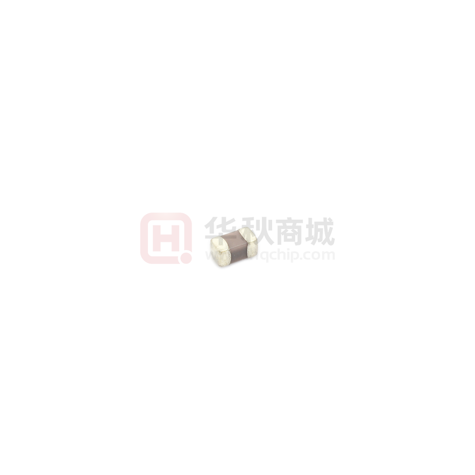
JMK063BC6105MP-F
【Notes】
・ This document is for reference use only and does not guarantee the specifications of the products.
・ The contents of this document are based on the existing April 1, 2020.
・ This document is subject to change for improvements or others without notice.
・ Please request and agree to the specification document of the products before purchasing and using them regardless of types of applications.
・ Please check and comply with the usage conditions and precautions described in this specification. Before use, please be sure to verify and validate the products under
intended operating environmental conditions with the products being installed in actual devices.
1.Scope
This specification shall apply to multilayer chip type ceramic capacitors used for general electronic equipment.
See basic information and precautions described in Section 6 for details.
2. Part Numbering System
Part number is indicated as follows:
(Example)
J
①
MK
063
②
B
③
C6
④
①Rated voltage
Code
J
105
Capacitance
M
⑤
P
⑥
-F
⑦
②Size
Voltage [VDC]
6.3 V
Code
063
L × W [mm]
0.6x0.3
③Control Code
Per Table 1
※△: space (blank)
④Temperature Characteristic
Code
C6
Reference standard
EIA
X6S
⑤Tolerance
Capacitance change rate
±22 %
Temperature range ※ Reference temperature
-55 to +105 ℃
25℃
Code
M
Tolerance
± 20 %
※Temperature range includes TC guarantee temperature range and operating temperature range.
⑥Thickness
Type
063
JMK063BC6105MP-F
Code
P
⑦Packaging
Thickness [mm]
0.3
Code
-F
Packaging type
Taping
MLCERMEE1900001
�Reference Specification
3.Shape, Structure, and Dimension
Figure 1: Shape and structure
No.
①
Name
Terminal Electrodes
(Surface)
Material
Sn Plating
②
Terminal Electrodes
③
④
⑤
External Electrodes
Internal Electrodes
Dielectric
Ni Plating
Cu Plating
Ni
Ni
Barium titanate
Table 1: Dimensions
Item type
063
Control
code※
B
L
0.6 ±0.09
Dimension [mm]
W
T
0.3 ±0.09
Per Table 2
e
0.15 ±0.05
※△: space (blank)
4.Rated Value
Table 2:Rated Value/Part Number List
Part number ※1
Temp. char ※1
JMK063BC6105MP-F
※1 conforms to EIA or JIS.
JMK063BC6105MP-F
X6S
Cap.
IR [min.]
DF [max]
Thickness [mm]
1 uF
100 MΩ·μF
10 %
0.3 ±0.09
Soldering method
Wave
Reflow
×
○
MLCERMEE1900001
�Reference Specification
5.Functions and Test Methods
Test Conditions:
Standard test conditions shall be temperature of 5 to 35°C, relative humidity of 45 to 85%, and air pressure of 86 to 106 kPa.
Tests shall be conducted at temperature of 25 ± 3°C, relative humidity of 60 to 70% and air pressure of 86 to 106 kPa if
test results are suspicious. Unless otherwise specified, all tests shall be conducted under the standard test conditions.
Item
No.
1
Specified Value
2
Operating Temperature
Range
Shape and Dimensions
Capable of continuous operation
within the range
Per Fig 1 and
Table 1
3
Heat Treatment
4
Voltage Treatment
5
No abnormality
6
Dielectric Withstanding Voltage
(between terminals)
Insulation Resistance (IR)
7
Capacitance (Cap.)
Per Table 2
Per Table 2
Remarks
-55 to +105 ℃
Initial value shall be measured after test sample is heat-treated at 150 +0/-10℃ for an hour
and kept at room temperature for 24±2hours
Initial value shall be measured after test sample is voltage-treated for an hour at temperature
and voltage which are specified as test conditions, and kept at room temperature for 24±2hours.
250% of DC rated voltage shall be applied for 1 to 5 seconds.
Charging and discharging current shall be 50mA or less.
Rated voltage shall be applied to test sample for 1 minute±5 seconds.
Charging and discharging current shall be 50mA or less
Heat treatment specified in this specification shall be conducted prior to measurement.
Measuring frequency and voltage shall conform to the table below.
Measuring Frequency
1kHz±10%
8
DF
Per Table 2
Heat treatment specified in this specification shall be conducted prior to measurement.
Measuring frequency and voltage shall conform to the table below.
Measuring Frequency
1kHz±10%
9
Temperature Characteristic
Per P.1 for ④
Measuring Voltage
0.5±0.1Vrms
Measuring Voltage
0.5±0.1Vrms
Heat treatment specified in this specification shall be conducted prior to measurement.
Maximum capacitance deviation in both (+) and (-) sides in range of lowest temperature to
highest temperature for capacitor shall be indicated in ratio of variation in reference to
capacitance value at reference temperature.
Measuring Voltage
1Vrms max
Special conditions exist.Please contact us for details.
JMK063BC6105MP-F
MLCERMEE1900001
�Reference Specification
Item
No
10
11
Adhesive Force of Terminal
Electrodes
Vibration
Specified Value
Terminal electrodes shall be no
exfoliation or a sign of exfoliation.
Initial performance shall be
satisfied
12
Solderability
More than 95% of terminal
electrode shall be covered with
fresh solder
13
Resistance to Appearance
Soldering
Heat
Cap. Change
No abnormality
Per Table 3
DF
Per Table 3
IR
Initial value shall be satisfied
Dielectric
No dielectric breakdown or damage
Thermal
Shock
(between terminals)
Appearance
No abnormality
Cap. Change
Per Table 3
DF
Per Table 3
IR
Initial value shall be satisfied
Dielectric
No dielectric breakdown or damage
Withstanding Voltage
(between terminals)
JMK063BC6105MP-F
Test sample shall be soldered to test board shown in Fig 2 and a force of 2N(200gf) shall be applied
for 30±5 seconds
Test sample shall be soldered to board shown in Fig 2.
Heat treatment specified in this specification shall be conducted prior to test
Test conditions: Frequency range: 10-55Hz
Overall amplitude: 1.5mm
Sweeping method: 10-55-10Hz for 1 min
Each two hours in X,Y,Z direction: 6 hours in total
【Eutectic】
Solder used shall be [JIS Z 3282 H60A or H63A].
Test sample shall be completely submerged in molten solder at 230±5℃ for 4±1 seconds
【Pb free】
Solder used shall be [Sn/3.0Ag/0.5Cu].
Test sample shall be completely submerged in molten solder at 245±3℃ for 4±1 seconds
Heat treatment specified in this specification shall be conducted prior to test.
Test sample shall be completely submerged in molten solder of 270±5℃ for 3±0.5 seconds.
Preheating as shown in the table below shall be continuously conducted before submersion and test
sample shall be kept at ambient temperature after test
Sequence Temperature[℃]
Time [min]
1
80 to 100
※
※ 021,~212:
2 to 5 min
2
150 to 200
※
316, 325, 432: 5 to 10 min
Measurement shall be conducted after test sample is kept at ambient temperature for 24±2 hours
Withstanding Voltage
14
Remarks
Test sample shall be soldered to board shown in Fig 2.
Heat treatment specified in this specification shall be conducted prior to test.
Test sample shall be exposed to each of temperature conditions in the following Steps
1 to 4 in sequence for the specified time
Sequence
Temperature[℃]
Time [min]
1
Lowest operating temperature
30±3
2
Ambient temperature
2~3
3
Highest operating temperature
30±3
4
Ambient temperature
2~3
Temperature cycle shall be repeated five times in this method, and measurement shall be conducted
after test sample is kept at ambient temperature for 24±2 hours.
MLCERMEE1900001
�Reference Specification
Item
No
15
Humidity
Specified Value
Appearance
No abnormality
Cap. Change
Per Table 3
DF
Per Table 3
IR
Initial value shall be satisfied
Remarks
Heat treatment specified in this specification shall be conducted prior to test.
Test sample shall be put into constant temperature/humidity bath at 40±2℃
and 90 to 95%RH for 500 +24/-0 hours
Measurement shall be conducted after test sample is kept at ambient temperature for 24±2 hours
(Steady State)
16
17
18
High
Appearance
Temperature
Loading
Cap. Change
Humidity
Loading
Bending
Strength
No abnormality
Per Table 3
DF
Per Table 3
IR
Initial value shall be satisfied
Appearance
No abnormality
Cap. Change
Per Table 3
DF
Per Table 3
IR
Initial value shall be satisfied
Appearance
No abnormality
Cap. Change
±12.5%
Table 3 Cap.,DF, and IR Changes after Test
Resistance to
Soldering Heat/
Thermal Shock
Part number
Cap.chg
DF
rate
[max]
JMK063BC6105MP-F ±15.0%
10%
※ Applied voltage : Ratio to rated voltage
JMK063BC6105MP-F
Voltage treatment specified in this specification shall be conducted prior to test
Test sample shall be put in thermostatic oven at maximum operating temperature and
DC voltage shall be continuously applied for 1000 +48/-0 hours
Applied DC voltage is described in Table 3.
Charging and discharging current shall be 50mA or less.
Measurement shall be conducted after test sample is kept at ambient temperature for 24±2 hours.
Voltage treatment specified in this specification shall be conducted prior to test
Test sample shall be put into constant temperature/humidity bath at 40±2℃ and 90 to 95%RH,
and DC rated voltage shall be continuously applied for 500 +24/-0 hours.
Charging and discharging current shall be 50mA or less
Measurement shall be conducted after test sample is kept at ambient temperature for 24±2 hours.
Test sample shall be soldered to test board as shown in Fig 3.
Sample shall be carefully soldered to avoid abnormality such as heat shock.
The board is bent 1.0mm for 10 seconds as shown in Fig 4.
Measurement shall be conducted as the board is bent 1.0mm
Humidity
(Steady state)
High Temperature Loading
Cap.chg
rate
DF
[max]
IR
[min]
Cap.chg
rate
DF
[max]
±25.0%
20%
10MΩ・μF
±25.0%
20%
Applied
voltage
※
150 %
Humidity Loading
IR
[min]
Cap.chg
rate
DF
[max]
IR
[min]
10MΩ・μF
±25.0%
20%
5MΩ・μF
MLCERMEE1900001
�Reference Specification
Fig. 2: Board / Test Jig of Adhesive Force of Terminal Electrodes, Vibration, and Thermal Shock
Size (L x W)
0.6x0.3
a
0.3
b
0.9
[mm]
c
0.3
Material: Glass epoxy board [JIS C 6484]
Copper foil (Thickness: 0.035mm)
Solder resist
Remarks: Uniform soldering shall be conducted with solder by using soldering iron or soldering oven.
Soldering shall be conducted with care to avoid abnormality such as heat shock.
Fig. 3: Board for Bending Strength Test
a
1±0.1
40
c
b
100
0.8
Material: Glass epoxy board [JIS C 6484]
Copper foil (Thickness: 0.035 mm)
Solder resist
[mm]
Size (L x W)
a
b
c
0.6x0.3
0.3
0.9
0.3
JMK063BC6105MP-F
MLCERMEE1900001
�6. Basic Information and Others
6-1.Basic Information
6-1-1. Equipment Intended for Use
The products listed in this specification are intended for general purpose and standard use in general electronic equipment (e.g., AV equipment, OA equipment, home electric
appliances, office equipment, information and communication equipment including, without limitation, mobile phone, and PC) and other equipment
specified in catalog or the individual product specification sheets.
TAIYO YUDEN has the line-up of the products intended for use in automotive electronic equipment, telecommunications infrastructure and industrial equipment,
or medical devices classified as GHTF Classes A to C (Japan Classes I to III).Therefore, when using our products for these equipment, please check available applications
specified in catalog or the individual product specification sheets and use the corresponding products.
6-1-2. Equipment Requiring Inquiry
Please be sure to contact TAIYO YUDEN for further information before using the products listed in this speciation for the following equipment (excluding intended
equipment as specified in catalog or the individual product specification sheets) which may cause loss of human life, bodily injury, serious property damage
and/or serious public impact due to a failure or defect of the products and/or malfunction attributed thereto.
(1) Transportation equipment (automotive powertrain control system, train control system, and ship control system, etc.)
(2) Traffic signal equipment
(3) Disaster prevention equipment, crime prevention equipment
(4) Medical devices classified as GHTF Class C (Japan Class III)
(5) Highly public information network equipment, data processing equipment (telephone exchange, and base station, etc.)
(6) Any other equipment requiring high levels of quality and/or reliability equal to the equipment listed above
6-1-3. Equipment Prohibited for Use
Please do not incorporate our products into the following equipment requiring extremely high levels of safety and/or reliability.
(1) Aerospace equipment (artificial satellite, rocket, etc.)
(2) Aviation equipment *1
(3) Medical devices classified as GHTF Class D (Japan Class IV), implantable medical devices *2
(4) Power generation control equipment (nuclear power, hydroelectric power, thermal power plant control system, etc.)
(5) Undersea equipment (submarine repeating equipment, underwater work equipment, etc.)
(6) Military equipment
(7) Any other equipment requiring extremely high levels of safety and/or reliability equal to the equipment listed above
RMV19001EFIX
�*Notes:
1. There is a possibility that our products can be used only for aviation equipment that does not directly affect the safe operation of aircraft
(e.g., in-flight entertainment, cabinlight, electric seat, cooking equipment) if such use meets requirements specified separately by TAIYO YUDEN. Please be sure
to contact TAIYO YUDEN for further information before using our products for such aviation equipment.
2. Implantable medical devices contain not only internal unit which is implanted in a body, but also external unit which is connected to the internal unit.
6-1-4. Limitation of Liability
Please note that unless you obtain prior written consent of TAIYO YUDEN, TAIYO YUDEN shall not be in any way responsible for any damages incurred by you or
third parties arising from use of the products listed in this specification for any equipment that is not intended for use by TAIYO YUDEN, or any equipment requiring inquiry to
TAIYO YUDEN or prohibited for use by TAIYO YUDEN as described above.
■ Safety Design
When using our products for high safety and/or reliability-required equipment or circuits, please fully perform safety and/or reliability evaluation. In addition,
please install (i) systems equipped with a protection circuit and a protection device and/or (ii) systems equipped with a redundant circuit or other system
to prevent an unsafe status in the event of a single fault for a failsafe design to ensure safety.
6-2. Precautions in Usage
・This specification does not cover the products when Sn-Zn lead free solder is used.
・When the products are used in places where dew condensation develops and/or where corrosive gas such as hydrogen sulfide, sulfurous acid, or chlorine exists
in the air, insulation (dielectric) deterioration may occur. Please do not use capacitors under such environmental conditions.
6-3. Storage Conditions
・Temperature and humidity in storage area shall be controlled carefully to maintain the solderability of terminal electrodes and to keep the packaging material in good
condition. Humidity should especially be kept as low as possible.
・The ambient temperature must be kept from 5 to 40°C. Even under ideal storage conditions, capacitor electrode solderability decreases with time. Therefore,
ceramic chip capacitors should be used within six (6) months from the time of delivery. If the period is exceeded, please check solderability before using the capacitors.
・The packaging material should be kept where no chlorine or sulfur exists in the air.
RMV19001EFIX
�6-4. RoHS Compliance
・The products conform to RoHS.
・“RoHS compliance” means that the products do not contain lead, cadmium, mercury,
hexavalent chromium, PBB ,PBDE ,DEHP,BBP,DBP,DIBP referring to Directive (EU )2015/863, except other non-restricted substances or impurities
which cannot be technically removed at refining process.
・The products are halogen-free products.
6-5. Resin Coating:
・Coating/molding capacitors with resin may have negative effects on the functions of the products.
・When the products are coated/molded with resin, please check effects on the products by analyzing them in actual applications/devices before use.
RMV19001EFIX
�7.Packaging
[Tape Packaging: 063 Type]
◎Tape packaging type: Paper tape
Dimensions
[Unit: mm]
A ※1
B ※1
0.37±0.06
0.39±0.06 ※2
0.44±0.06 ※3
0.67±0.06
0.69±0.06 ※2
0.74±0.06 ※3
Dimensions
[Unit: mm]
C
D
E
F
G
H
8.0±0.3
3.5±0.05
1.75±0.1
2.0±0.05
2.0±0.05
4.0±0.1
t
J
φ1.5
+0.1
-0
t1 ※1
0.45max
0.42max
0.50max ※2
0.65max ※3
0.45max ※2
0.50max ※3
※1. A, B,t1: Sufficient clearance
※2. *MK063A********F
※3. *MK063B********F
RMV19001EFIX
�[Tape Packaging: 063 Type]
Dimensions of Reel
[Unit: mm]
A
B
C
D
E
W
t
R
φ178±2.0
φ50min.
φ13.0±0.2
φ21.0±0.8
2.0±0.5
10.0±1.5
2.5max.
1.0
RMV19001EFIX
�1) Taping shall be right-sided wound. Sprocket hole shall be on the right side against the pull-out direction.
2) Either the width side (W) or the thickness side (t) of the products below faces up at random when the products
are inserted in the chip cavities:
3) There shall be blank spaces in each reel tape as shown in the following figure.
・Leader part
400mm min.
・Leader part (Blank part)
100mm min.
・Trailer (Blank part)
160mm min.
4) Neither top/bottom tapes of paper tape nor top tape of embossed tape shall cover sprocket holes.
5) There shall be no seam on paper tape or embossed tape.
6) Tensile strength of the tape shall be 5N (0.51 kgf) or over.
7) The number of the chip missing from tape reel shall be one (1) piece at a maximum per reel.
8) The number of packaged chips per reel is 15,000 pieces.
9) Label indicating part No., quantity and control No. shall be attached to the outside of each reel.
10) Peeling strength of top tape shall be 0.1 to 0.7N (10.2 to 71.4 gf) when top tape is peeled from carrier tape at
an angle of 0 to 20 degrees.
0 to 20°
RMV19001EFIX
�■PRECAUTIONS
1. Circuit Design
Precautions
◆Verification of operating environment, electrical rating and performance
1. A malfunction of equipment in fields such as medical, aerospace, nuclear control, etc. may cause serious harm to human life or have severe social
ramifications.
Therefore, any capacitors to be used in such equipment may require higher safety and reliability, and shall be clearly differentiated from them used
in general purpose applications.
◆Operating Voltage (Verification of Rated voltage)
1. The operating voltage for capacitors must always be their rated voltage or less.
If an AC voltage is loaded on a DC voltage, the sum of the two peak voltages shall be the rated voltage or less.
For a circuit where an AC or a pulse voltage may be used, the sum of their peak voltages shall also be the rated voltage or less.
2. Even if an applied voltage is the rated voltage or less reliability of capacitors may be deteriorated in case that either a high frequency AC voltage or
a pulse voltage having rapid rise time is used in a circuit.
2. PCB Design
◆Pattern configurations (Design of Land-patterns)
1. When capacitors are mounted on PCBs, the amount of solder used (size of fillet) can directly affect the capacitor performance. Therefore, the
following items must be carefully considered in the design of land patterns:
(1)Excessive solder applied can cause mechanical stresses which lead to chip breaking or cracking. Therefore, please consider appropriate
land-patterns for proper amount of solder.
(2)When more than one component are jointly soldered onto the same land, each component's soldering point shall be separated by solder-resist.
◆Pattern configurations (Capacitor layout on PCBs)
After capacitors are mounted on boards, they can be subjected to mechanical stresses in subsequent manufacturing processes (PCB cutting, board
inspection, mounting of additional parts, assembly into the chassis, wave soldering of the boards, etc.). For this reason, land pattern configurations
and positions of capacitors shall be carefully considered to minimize stresses
Precautions
.
RMV19001EFIX
�◆Pattern configurations (Design of Land-patterns)
The following diagrams and tables show some examples of recommended land patterns to prevent excessive solder amounts.
(1)Recommended land dimensions for typical chip capacitors
● Multilayer Ceramic Capacitors : Recommended land
Land patterns for PCBs
Land pattern
dimensions
Solder-resist
Chip capacitor
(unit: mm)
Wave-soldering
C
Type
107
212
316
325
L
1.6
2.0
3.2
3.2
Size
B
A
B
W
0.8
1.25
1.6
2.5
A
0.8 to 1.0 1.0 to 1.4 1.8 to 2.5 1.8 to 2.5
Chip capacitor
B
0.5 to 0.8 0.8 to 1.5 0.8 to 1.7 0.8 to 1.7
C
0.6 to 0.8 0.9 to 1.2 1.2 to 1.6 1.8 to 2.5
W
L
Technical
considerati
ons
Reflow-soldering
Type
021
042
063
105
107
212
316
325
432
L
0.25
0.4
0.6
1.0
1.6
2.0
3.2
3.2
4.5
Size
W
0.125
0.2
0.3
0.5
0.8
1.25
1.6
2.5
3.2
0.095〜
0.15〜
0.20〜
0.45〜
A
0.8〜1.0 0.8〜1.2 1.8〜2.5 1.8〜2.5 2.5〜3.5
0.135
0.25
0.30
0.55
0.085〜
0.15〜
0.20〜
0.40〜
B
0.6〜0.8 0.8〜1.2 1.0〜1.5 1.0〜1.5 1.5〜1.8
0.125
0.20
0.30
0.50
0.110〜
0.15〜
0.25〜
0.45〜
C
0.6〜0.8 0.9〜1.6 1.2〜2.0 1.8〜3.2 2.3〜3.5
0.150
0.30
0.40
0.55
Note:Recommended land size might be different according to the allowance of the size of the product.
● LWDC:
Recommended
land
dimensions
reflow-soldering
(unit: mm)
Type
105
107
212
L
0.52
0.8
1.25
Size
W
1.0
1.6
2.0
A
0.18〜 0.25〜0.3 0.5〜0.7
0.22
B
0.2〜0.25 0.3〜0.4 0.4〜0.5
C
0.9〜1.1 1.5〜1.7 1.9〜2.1
for
LWDC
W
L
RMV19001EFIX
�(2)Examples of good and bad solder application
Item
Not recommended
Lead wire of component
Recommended
Solder-resist
Mixed mounting of SMD
and leaded components
Chassis
Solder (for grounding)
Solder-resist
Component placement
close to the chassis
Electrode pattern
Lead wire of component
Hand-soldering of
leaded components
near mounted
components
Soldering iron
Solder-resist
Solder-resist
Horizontal component
placement
RMV19001EFIX
�◆Pattern configurations (Capacitor layout on PCBs)
1-1. The following is examples of good and bad capacitor layouts ; capacitors shall be located to minimize any
board warp or deflection.
Items
Not recommended
Recommended
Place the product at a
right angle to the
Deflection of
direction of the
board
anticipated
mechanical stress.
possible mechanical stresses from
1-2. The amount of mechanical stresses given will vary depending on capacitor layout. Please refer to diagram below.
E
D
Perforation
C
A
B
Slit
Magnitude of stress
A>B=C>D>E
1-3. When PCB is split, the amount of mechanical stress on the capacitors can vary according to the method used. The following methods are listed in
order from least stressful to most stressful: push-back, slit, V-grooving, and perforation. Thus, please consider the PCB, split methods as well as
chip location.
RMV19001EFIX
�3. Mounting
Precautions
◆Adjustment of mounting machine
1. When capacitors are mounted on PCB, excessive impact load shall not be imposed on them.
2. Maintenance and inspection of mounting machines shall be conducted periodically.
◆Selection of Adhesives
1. When chips are attached on PCBs with adhesives prior to soldering, it may cause capacitor characteristics degradation unless the following factors
are appropriately checked : size of land patterns, type of adhesive, amount applied, hardening temperature and hardening period. Therefore,
please contact us for further information.
◆Adjustment of mounting machine
1. When the bottom dead center of a pick-up nozzle is too low, excessive force is imposed on capacitors and causes damages. To avoid this, the
following points shall be considerable.
(1)The bottom dead center of the pick-up nozzle shall be adjusted to the surface level of PCB without the board deflection.
(2)The pressure of nozzle shall be adjusted between 1 and 3 N static loads.
(3)To reduce the amount of deflection of the board caused by impact of the pick-up nozzle, supporting pins or back-up pins shall be used on
the other side of the PCB. The following diagrams show some typical examples of good and bad pick-up nozzle placement:
Item
Improper method
Proper method
Single-sided
mounting
chipping
or cracking
supporting pins
or back-up pins
Technical
considerati
ons
Double-sided
mounting
chipping
or cracking
supporting pins
or back-up pins
2. As the alignment pin is worn out, adjustment of the nozzle height can cause chipping or cracking of capacitors because of mechanical impact on the
capacitors.
To avoid this, the monitoring of the width between the alignment pins in the stopped position, maintenance, check and replacement of the pin
shall be conducted periodically.
◆Selection of Adhesives
Some adhesives may cause IR deterioration. The different shrinkage percentage of between the adhesive and the capacitors may result in stresses on
the capacitors and lead to cracking. Moreover, too little or too much adhesive applied to the board may adversely affect components. Therefore, the
following precautions shall be noted in the application of adhesives.
RMV19001EFIX
�(1)Required adhesive characteristics
a. The adhesive shall be strong enough to hold parts on the board during the mounting & solder process.
b. The adhesive shall have sufficient strength at high temperatures.
c. The adhesive shall have good coating and thickness consistency.
d. The adhesive shall be used during its prescribed shelf life.
e. The adhesive shall harden rapidly.
f. The adhesive shall have corrosion resistance.
g. The adhesive shall have excellent insulation characteristics.
h. The adhesive shall have no emission of toxic gasses and no effect on the human body.
(2)The recommended amount of adhesives is as follows;
[Recommended condition]
After capacitor are
Amount adhesive
a
a
bonded
Figur
212/316 case sizes as examples
e
b
a
0.3mm min
b
100 to 120μm
c
Adhesives shall not contact land
c
c
4. Soldering
Precautions
◆Selection of Flux
Since flux may have a significant effect on the performance of capacitors, it is necessary to verify the following conditions prior to use;
(1)Flux used shall be less than or equal to 0.1 wt%( in Cl equivalent) of halogenated content. Flux having a strong acidity content shall not be
applied.
(2)When shall capacitors are soldered on boards, the amount of flux applied shall be controlled at the optimum level.
(3)When water-soluble flux is used, special care shall be taken to properly clean the boards.
◆Soldering
Temperature, time, amount of solder, etc. shall be set in accordance with their recommended conditions.
Sn-Zn solder paste can adversely affect MLCC reliability.
Please contact us prior to usage of Sn-Zn solder.
Technical
considerati
ons
◆Selection of Flux
1-1. When too much halogenated substance(Chlorine, etc.) content is used to activate flux, or highly acidic flux is used, it may lead to corrosion of
terminal electrodes or degradation of insulation resistance on the surfaces of the capacitors.
1-2. Flux is used to increase solderability in wave soldering. However if too much flux is applied, a large amount of flux gas may be emitted and may
adversely affect the solderability. To minimize the amount of flux applied, it is recommended to use a flux-bubbling system.
1-3. Since the residue of water-soluble flux is easily dissolved in moisture in the air, the residues on the surfaces of capacitors in high humidity
conditions may cause a degradation of insulation resistance and reliability of the capacitors. Therefore, the cleaning methods and the capability
of the machines used shall also be considered carefully when water-soluble flux is used.
RMV19001EFIX
�◆Soldering
・ Ceramic chip capacitors are susceptible to thermal shock when exposed to rapid or concentrated heating or rapid cooling.
・ Therefore, the soldering must be conducted with great care so as to prevent malfunction of the components due to excessive thermal shock.
・ Preheating : Capacitors shall be preheated sufficiently, and the temperature difference between the capacitors and solder shall be within 130℃.
・ Cooling : The temperature difference between the capacitors and cleaning process shall not be greater than 100℃.
[Reflow soldering]
【Recommended conditions for
eutectic soldering】
【Recommended condition for
Pb-free soldering】
300
300
200
60sec. 60sec
Min.
Min.
Peak
260℃ Max.
Within 10sec.
230℃
Within 10sec.
Slow cooling
100
Temperature(℃)
Temperature(℃)
Preheating
0
200
Slow
cooling
100
0
Preheating150℃ Heating above
230℃
60sec. Min.
40sec. Max.
1/2T~1/3T
Caution
①The ideal condition is to have solder mass(fillet)controlled to 1/2 to
1/3 of the thickness of a capacitor.
②Because excessive dwell times can adversely affect solderability,
soldering duration shall be kept as close to recommended times as
possible. soldering for 2 times.
[Wave soldering]
【Recommended conditions for
eutectic soldering】
Slow cooling
100
0
Temperature(℃)
Temperature(℃)
300
230~250℃
Within 3sec.
200
Solder
T
PC board
【Recommended condition for
Pb-free soldering】
300
Preheating
120sec. Min.
Capacitor
200
100
120sec. Min.
Peak
260℃ Max.
Within 10sec.
Preheating
150℃
Slow
cooling
0
Caution
①Wave soldering must not be applied to capacitors designated as for reflow soldering only. soldering for 1
times.
RMV19001EFIX
�【Recommended condition for
Pb-free soldering】
400
400
300
200
Slow cooling
100
0
Preheating
60sec. Min.
Temperature(℃)
Temperature(℃)
300
⊿T
Slow cooling
200
100
0
400
Peak
350℃ Max.
Within 3sec.
230~280℃
Within 3sec.
Preheating
150℃ Min.
200
100
60sec. Min.
316type or less
0
⊿T
⊿T≦150℃
Peak
280℃ Max.
Within 3sec.
300
温度(℃)
[Hand soldering]
【Recommended conditions for
eutectic soldering】
325type
more
Slow cooling
⊿T
Preheating
150℃ Min.
60sec. Min.
or
⊿T
⊿T≦130℃
Caution
① Use a 20W soldering iron with a maximum tip diameter of 1.0 mm.
②
The soldering iron shall not directly touch capacitors. soldering for 1 times.
5. Cleaning
Precautions
◆Cleaning conditions
1. When PCBs are cleaned after capacitors mounting, please select the appropriate cleaning solution in accordance with the intended use of the
cleaning. (e.g. to remove soldering flux or other materials from the production process.)
2. Cleaning condition shall be determined after it is verified by using actual cleaning machine that the cleaning process does not affect capacitor's
characteristics.
Technical
considerati
ons
1. The use of inappropriate cleaning solutions can cause foreign substances such as flux residue to adhere to capacitors or deteriorate their outer
coating, resulting in a degradation of the capacitor's electrical properties (especially insulation resistance).
2. Inappropriate cleaning conditions( insufficient or excessive cleaning) may adversely affect the performance of the capacitors.
In the case of ultrasonic cleaning, too much power output can cause excessive vibration of PCBs which may lead to the cracking of capacitors or
the soldered portion, or decrease the terminal electrodes' strength. Therefore, the following conditions shall be carefully checked;
Ultrasonic output :
20 W/ℓ or les
Ultrasonic frequency :
40 kHz or less
Ultrasonic washing period : 5 min. or less
6. Resin coating and mold
Precautions
1. With some type of resins, decomposition gas or chemical reaction vapor may remain inside the resin during the hardening period or while left under
normal storage conditions resulting in the deterioration of the capacitor's performance.
2. When a resin's hardening temperature is higher than capacitor's operating temperature, the stresses generated by the excessive heat may lead to
damage or destruction of capacitors.
The use of such resins, molding materials etc. is not recommended.
RMV19001EFIX
�7. Handling
Precautions
◆Splitting of PCB
1. When PCBs are split after components mounting, care shall be taken so as not to give any stresses of deflection or twisting to the board.
2. Board separation shall not be done manually, but by using the appropriate devices.
◆Mechanical considerations
Be careful not to subject capacitors to excessive mechanical shocks.
(1)If ceramic capacitors are dropped onto a floor or a hard surface, they shall not be used.
(2)Please be careful that the mounted components do not come in contact with or bump against other boards or components.
8. Storage conditions
Precautions
◆Storage
1. To maintain the solderability of terminal electrodes and to keep packaging materials in good condition, care must be taken to control temperature
and humidity in the storage area. Humidity should especially be kept as low as possible.
・Recommended conditions
Ambient temperature : Below 30℃
Humidity : Below 70% RH
The ambient temperature must be kept below 40℃. Even under ideal storage conditions, solderability of capacitor is deteriorated as time passes,
so capacitors shall be used within 6 months from the time of delivery.
・Ceramic chip capacitors shall be kept where no chlorine or sulfur exists in the air.
2. The capacitance values of high dielectric constant capacitors will gradually decrease with the passage of time, so care shall be taken to design
circuits. Even if capacitance value decreases as time passes, it will get back to the initial value by a heat treatment at 150℃ for 1hour.
Technical
considerati
ons
If capacitors are stored in a high temperature and humidity environment, it might rapidly cause poor solderability due to terminal oxidation and quality
loss of taping/packaging materials. For this reason, capacitors shall be used within 6 months from the time of delivery. If exceeding the above period,
please check solderability before using the capacitors.
※RCR-2335(Safety Application Guide for fixed ceramic capacitors for use in electronic equipment)is published by JEITA.
Please check the guide regarding precautions for deflection test, soldering by spot heat, and so on.
RMV19001EFIX
�


 工商网监
湘ICP备2023018690号
工商网监
湘ICP备2023018690号

