TAK CHEONG
®
SEM IC O N DU C TO R
Plastic Package
N-Channel 1.8-V (G-S) MOSFET
3
TA = 25°C unless otherwise noted
Absolute Maximum Ratings
Symbol
Green Product
Parameter
5 secs
Steady State
Units
2
VDS
Drain-Source Voltage
20
V
VGS
Gate-Source Voltage
±6V
V
ID
Continuous Drain Current
e
Pulsed Drain Current
IS
Continuous Source Current
TSTG
TJ
ESD
Power Dissipation
600
400
d
IDM
PD
TA=25℃
TA=85℃
e
500
350
1000
mA
mA
e
275
250
mA
TA=25℃
TA=85℃
175
90
150
80
mW
Storage Temperature Range
Operating Junction Temperature
Gate-source ESD Rating
(HBM, Method 3015)
-55 to +150
°C
+150
°C
2000
V
1. Gate
2. Source
3. Drain
1
SOT-523
These ratings are limiting values above which the serviceability of the device may be impaired.
Notes:
d.
Pulse width limited by maximum junction temperature.
e.
Surface mounted on FR4 board.
FEATURES
z
z
z
z
z
z
z
z
z
z
z
Electrical Symbol:
TrenchFET ®Power MOSFET: 1.8-V Rated
Gate-Source ESD Protected: 2000V
High-side Switching
Low On-Resistance: 0.7Ω
Low Threshold: 0.8V (Typ.)
Fast Switching Speed: 10ns
S-Prefix for Automotive and Other Applications
Requiring Unique Site and Control Change
Requirements
RoHS Compliant
Green EMC
Matte Tin(Sn) Lead Finish
Weight: approx. 0.002g
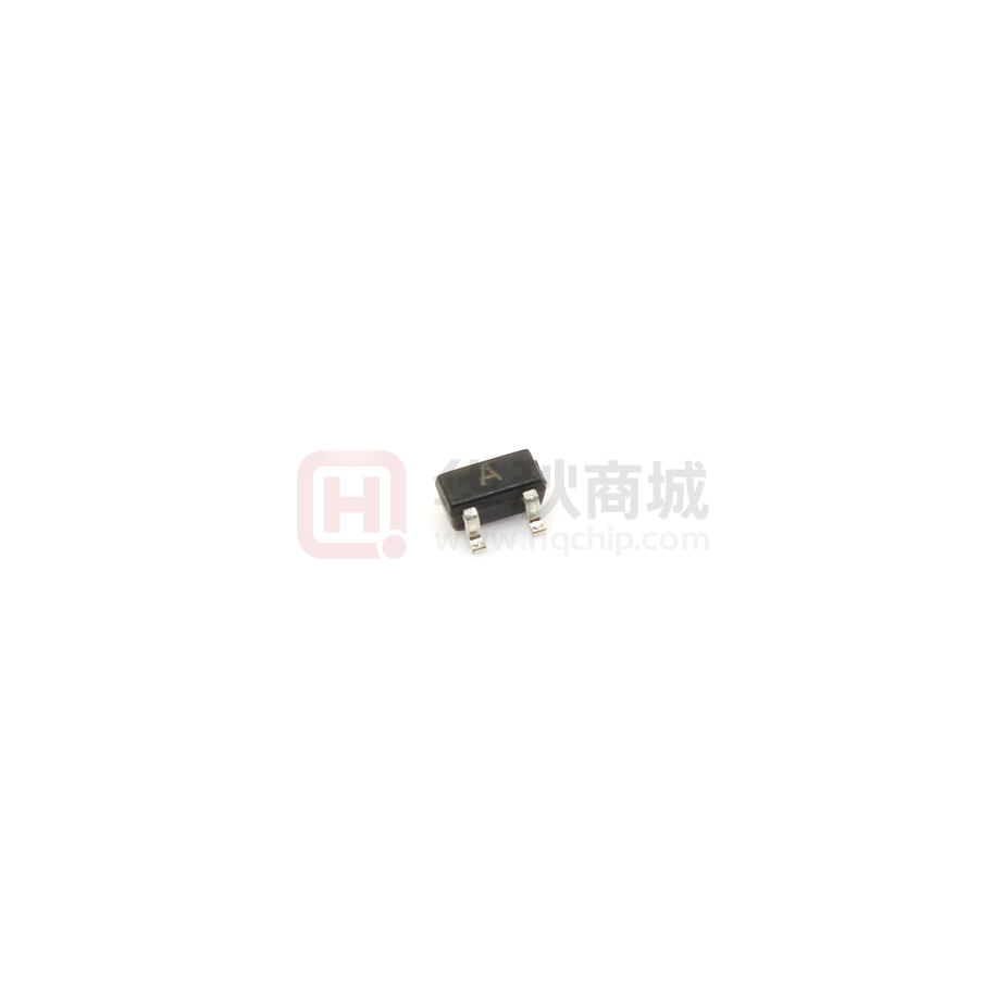
Device Marking Code:
A
BENEFITS
z
z
z
z
z
Ease in Driving Switches
Low Offset(Error) Voltage
Low-Voltage operation
High-Speed Circuits
Low Battery Voltage Operation
APPLICATIONS
z
z
z
z
Drivers: Relays, Solenoids, Lamps, Hammers, displays, Memories
Battery Operated Systems
Power Supply Converter Circuits
Load/Power Switching Cell Phones, agers
DB Number: DB-270
March 2015, Revision A
Page 1
LSI1012XT1G
150mW SOT-523 SURFACE MOUNT
�TAK CHEONG
SEM IC O N DU C TO R
Electrical Characteristics (TA = 25°C unless otherwise noted)
Static
Symbol
Parameter
Test Condition
Limits
Min
Typ
Gate-Threshold Voltage
VDS= VGS, ID=250uA
IGSS
Gate-Body Leakage
VDS=0V, VGS=±4.5V
IDSS
Zero Gate Voltage Drain Current
VDS=20V, VGS=0V
ID(ON)
On-state Drain Current a
VDS=5V, VGS=4.5V
Drain-Source On-Resistance a
VGS=4.5V, ID=600mA
0.41
0.70
VGS=2.5V, ID=500mA
0.53
0.85
VGS=1.8V, ID=350mA
0.70
1.25
VDS=10V, ID=400mA
1
Vth(GS)
RDS(on)
gfs
Forward Trans Conductance
VSD
Diode Forward Voltage
a
a
0.45
Max
0.9
Volts
±0.5
±1.0
uA
0.3
100
nA
700
mA
0.8
IS=150mA, VGS=0V
Unit
Ω
ms
1.2
V
Dynamic b
Parameter
Symbol
Test Condition
Limits
Min
Typ
Max
--
750
--
--
75
--
Qg
Total Gate Charge
Qgs
Gate-Source Charge
Qgd
Gate-Drain Charge
--
225
--
Turn-On Delay Time
--
5
--
--
5
--
--
25
--
--
11
--
Td(on)
tr
td(off)
tf
Rise Time
Turn-Off Delay Time
Fall Time
VDS=10V, VGS=4.5V,
ID=250mA
VDD=10V, RL=47Ω,
ID=200mA, VGEN=4.5V
RG=10Ω
Unit
pC
ns
Notes:
a.
Pulse test: pulse width≤300us, duty cycle ≤2%.
b.
Guaranteed by design, not subject to production testing.
DB Number: DB-270
March 2015, Revision A
Page 2
�TAK CHEONG
SEM IC O N DU C TO R
SOT-523 Package Outline
DIM
Typical Soldering Pattern:
MILLIMETERS
INCHES
MIN
MAX
MIN
MAX
A
0.70
0.90
0.028
0.035
A1
0.00
0.10
0.000
0.004
A2
0.70
0.80
0.028
0.031
b1
0.15
0.25
0.006
0.010
b2
0.25
0.35
0.010
0.014
c
0.10
0.20
0.004
0.008
D
1.50
1.70
0.059
0.067
E
0.70
0.90
0.028
0.035
E1
1.45
1.75
0.057
0.069
e
e1
0.50 TYP.
0.90
L
0.020 TYP.
1.10
0.035
0.40 REF.
L1
0.10
θ
0
O
0.043
0.016 REF.
0.30
8
O
0.004
0
O
0.012
8
O
NOTES:
1. Above package outline conforms to JEITA EAIJ ED-7500A SC-75A.
2. Dimensions are exclusive of Burrs, Mold Flash & Tie Bar extrusions.
DB Number: DB-270
March 2015, Revision A
Page 3
�TAK CHEONG
®
DISC LA I MER NOTIC E
NOTICE
The information presented in this document is for reference only. Tak Cheong reserves the right to make
changes without notice for the specification of the products displayed herein.
The product listed herein is designed to be used with ordinary electronic equipment or devices, and not
designed to be used with equipment or devices which require high level of reliability and the malfunction of with
would directly endanger human life (such as medical instruments, transportation equipment, aerospace
machinery, nuclear-reactor controllers, fuel controllers and other safety devices), Tak Cheong Semiconductor
Co., Ltd., or anyone on its behalf, assumes no responsibility or liability for any damagers resulting from such
improper use of sale.
This publication supersedes & replaces all information reviously supplied. For additional information, please visit
our website http://www.takcheong.com, or consult your nearest Tak Cheong’s sales office for further assistance.
Number: DB-100
April 14, 2008 / A
�
很抱歉,暂时无法提供与“LSI1012XT1G”相匹配的价格&库存,您可以联系我们找货
免费人工找货- 国内价格
- 10+0.10728
- 50+0.09923
- 200+0.09253
- 600+0.08582
- 1500+0.08046
- 3000+0.07711


 工商网监
湘ICP备2023018690号
工商网监
湘ICP备2023018690号
