SIOV metal oxide varistors
SMD varistors standard series, CU types
Series/Type:
B726*
Date:
January 2018
© EPCOS AG 2018. Reproduction, publication and dissemination of this publication, enclosures hereto and the
information contained therein without EPCOS' prior express consent is prohibited.
EPCOS AG is a TDK Group Company.
�SMD varistors (CU types)
B726*
Standard series
EPCOS type designation system for SMD varistor standard series
CU
4032
K
Construction:
CU � Encapsulated chip
Case sizes:
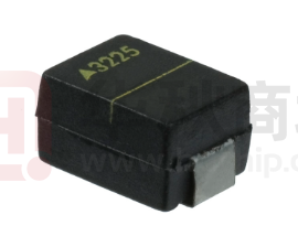
3225 � 32 x 25
4032 � 40 x 32
Varistor voltage tolerance:
K � ±10%
Maximum RMS operating voltage (VRMS):
275 � 275 V
Taping mode:
G2 � Taped, 330-mm reel
Please read Cautions and warnings and
Important notes at the end of this document.
Page 2 of 23
275
G2
�SMD varistors (CU types)
B726*
Standard series
Construction
Cylindrical varistor element, encapsulated.
Encapsulation: thermoplastic, flame-retardant to UL 94 V-0.
Termination: tinned copper alloy, suitable for lead-free wave and reflow
soldering, and compatible with tin/lead solder.
Features
Electrical equivalents to leaded types SIOV-S05/S07
Operating voltage up to 300 VRMS
SMD plastic package
RoHS-compatible
Suitable for lead-free soldering
PSpice models available
Approvals
UL
IEC
CSA approved (types with voltages higher than 30 VRMS)
Delivery mode
Blister tape, 330-mm reel
Packing unit: 1000 pcs.
V/I characteristics and derating curves
V/I and derating curves are attached to the data sheet. The curves are sorted by VRMS and
then by case size, which is included in the type designation.
General technical data
Maximum RMS operating voltage
Maximum DC operating voltage
Maximum surge current
Maximum energy absorption
Maximum clamping voltage
Operating temperature
Storage temperature
Please read Cautions and warnings and
Important notes at the end of this document.
(8/20 µs) 1 time
(2 ms)
(8/20 µs)
Page 3 of 23
VRMS
VDC
imax
Wmax
vc,max
11 ... 300
14 ... 385
100 ... 1200
300 ... 23000
36 ... 775
�40/+85
�40/+125
V
V
A
mJ
V
°C
°C
�SMD varistors (CU types)
B726*
Standard series
Temperature derating
Climatic category: �40/+85 °C
Please read Cautions and warnings and
Important notes at the end of this document.
Page 4 of 23
�SMD varistors (CU types)
B726*
Standard series
Electrical specifications and ordering codes
Maximum ratings (TA = 85 °C)
imax
(8/20 µs)
1 time
V
V
A
CU3225K11G2
B72650M0110K072
11
14
100
CU4032K11G2
B72660M0110K072
11
14
250
CU3225K14G2
B72650M0140K072
14
18
100
CU4032K14G2
B72660M0140K072
14
18
250
CU3225K17G2
B72650M0170K072
17
22
100
CU4032K17G2
B72660M0170K072
17
22
250
CU3225K20G2
B72650M0200K072
20
26
100
CU4032K20G2
B72660M0200K072
20
26
250
CU3225K25G2
B72650M0250K072
25
31
100
CU4032K25G2
B72660M0250K072
25
31
250
CU3225K30G2
B72650M0300K072
30
38
100
CU4032K30G2
B72660M0300K072
30
38
250
CU3225K35G2
B72650M0350K072
35
45
100
CU4032K35G2
B72660M0350K072
35
45
250
CU3225K40G2
B72650M0400K072
40
56
100
CU4032K40G2
B72660M0400K072
40
56
250
CU3225K50G2
B72650M0500K072
50
65
400
CU4032K50G2
B72660M0500K072
50
65
1200
CU3225K60G2
B72650M0600K072
60
85
400
CU4032K60G2
B72660M0600K072
60
85
1200
CU3225K75G2
B72650M0750K072
75
100
400
CU4032K75G2
B72660M0750K072
75
100
1200
CU3225K95G2
B72650M0950K072
95
125
400
CU4032K95G2
B72660M0950K072
95
125
1200
CU3225K115G2
B72650M0111K072
115
150
400
CU4032K115G2
B72660M0111K072
115
150
1200
CU3225K130G2
B72650M0131K072
130
170
400
CU4032K130G2
B72660M0131K072
130
170
1200
CU3225K140G2
B72650M0141K072
140
180
400
CU4032K140G2
B72660M0141K072
140
180
1200
CU3225K150G2
B72650M0151K072
150
200
400
CU4032K150G2
B72660M0151K072
150
200
1200
CU3225K175G2
B72650M0171K072
175
225
400
CU4032K175G2
B72660M0171K072
175
225
1200
1)
Note: Nominal discharge current In according to UL 1449, 4th edition.
Type
Ordering code
Please read Cautions and warnings and
Important notes at the end of this document.
VRMS
VDC
Page 5 of 23
In1)
(8/20 µs)
15 times
A
50
100
50
100
50
100
50
100
50
100
50
100
50
100
50
100
150
500
150
500
150
500
150
500
150
500
150
500
150
500
150
500
150
500
Wmax Pmax
(2 ms)
mJ
300
800
400
900
500
1100
600
1300
700
1600
900
2000
1100
2500
1300
3000
1800
4200
2200
4800
2500
5900
3400
7600
3600
8400
4200
9500
4500
10000
4900
11000
5600
13000
mW
10
20
10
20
10
20
10
20
10
20
10
20
10
20
10
20
100
250
100
250
100
250
100
250
100
250
100
250
100
250
100
250
100
250
�SMD varistors (CU types)
B726*
Standard series
Characteristics (TA = 25 °C)
Type
CU3225K11G2
CU4032K11G2
CU3225K14G2
CU4032K14G2
CU3225K17G2
CU4032K17G2
CU3225K20G2
CU4032K20G2
CU3225K25G2
CU4032K25G2
CU3225K30G2
CU4032K30G2
CU3225K35G2
CU4032K35G2
CU3225K40G2
CU4032K40G2
CU3225K50G2
CU4032K50G2
CU3225K60G2
CU4032K60G2
CU3225K75G2
CU4032K75G2
CU3225K95G2
CU4032K95G2
CU3225K115G2
CU4032K115G2
CU3225K130G2
CU4032K130G2
CU3225K140G2
CU4032K140G2
CU3225K150G2
CU4032K150G2
CU3225K175G2
CU4032K175G2
VV
(1 mA)
V
18
18
22
22
27
27
33
33
39
39
47
47
56
56
68
68
82
82
100
100
120
120
150
150
180
180
205
205
220
220
240
240
270
270
Please read Cautions and warnings and
Important notes at the end of this document.
∆VV
vc,max
%
±10
±10
±10
±10
±10
±10
±10
±10
±10
±10
±10
±10
±10
±10
±10
±10
±10
±10
±10
±10
±10
±10
±10
±10
±10
±10
±10
±10
±10
±10
±10
±10
±10
±10
V
36
36
43
43
53
53
65
65
77
77
93
93
110
110
135
135
135
135
165
165
200
200
250
250
300
300
340
340
360
360
395
395
455
455
Page 6 of 23
Ic
(8/20 µs)
A
1.0
2.5
1.0
2.5
1.0
2.5
1.0
2.5
1.0
2.5
1.0
2.5
1.0
2.5
1.0
2.5
5.0
10.0
5.0
10.0
5.0
10.0
5.0
10.0
5.0
10.0
5.0
10.0
5.0
10.0
5.0
10.0
5.0
10.0
Ctyp
(1 kHz, 1 V)
pF
1750
2750
1450
2300
1200
1900
980
1600
850
1400
720
1200
620
1050
520
900
300
530
250
480
210
430
135
260
110
220
100
200
95
180
90
170
75
150
�SMD varistors (CU types)
B726*
Standard series
Electrical specifications and ordering codes
Maximum ratings (TA = 85 °C)
imax
(8/20 µs)
1 time
V
V
A
CU3225K230G2
B72650M0231K072
230
300
400
CU4032K230G2
B72660M0231K072
230
300
1200
CU3225K250G2
B72650M0251K072
250
320
400
CU4032K250G2
B72660M0251K072
250
320
1200
CU3225K275G2
B72650M0271K072
275
350
400
CU4032K275G2
B72660M0271K072
275
350
1200
CU3225K300G2
B72650M0301K072
300
385
400
CU4032K300G2
B72660M0301K072
300
385
1200
1)
Note: Nominal discharge current In according to UL 1449, 4th edition.
Type
Ordering code
VRMS
VDC
In1)
(8/20 µs)
15 times
A
150
500
150
500
150
500
150
500
Wmax Pmax
(2 ms)
mJ
7200
17000
8200
19000
8600
21000
9600
23000
mW
100
250
100
250
100
250
100
250
Characteristics (TA = 25 °C)
Type
CU3225K230G2
CU4032K230G2
CU3225K250G2
CU4032K250G2
CU3225K275G2
CU4032K275G2
CU3225K300G2
CU4032K300G2
VV
(1 mA)
V
360
360
390
390
430
430
470
470
Please read Cautions and warnings and
Important notes at the end of this document.
∆VV
vc,max
%
±10
±10
±10
±10
±10
±10
±10
±10
V
595
595
650
650
710
710
775
775
Page 7 of 23
Ic
(8/20 µs)
A
5.0
10.0
5.0
10.0
5.0
10.0
5.0
10.0
Ctyp
(1 kHz, 1 V)
pF
60
115
55
105
50
95
45
90
�SMD varistors (CU types)
B726*
Standard series
Dimensional drawing
Dimensions in mm
Chip size VRMS,max
EIA in mm
l
w
h
3225
11 ... 175
8.0 ±0.3
6.3 ±0.3 3.2 ±0.3
3225
230 ... 300 8.0 ±0.3
6.3 ±0.3 4.5 ±0.3
4032
11 ... 175
4032
230 ... 300 10.2 ±0.3 8.0 ±0.3 4.5 ±0.3
10.2 ±0.3 8.0 ±0.3 3.2 ±0.3
Recommended solder pad layout
Dimensions in mm
Please read Cautions and warnings and
Important notes at the end of this document.
Chip size
EIA in mm
A
B
C
3225
3.50
2.80
4.50
4032
3.50
2.80
6.50
Page 8 of 23
�SMD varistors (CU types)
B726*
Standard series
Delivery mode
EIA case size Taping
3225
3225
3225
3225
3225
3225
3225
3225
3225
3225
3225
3225
3225
3225
3225
3225
3225
3225
3225
3225
3225
4032
4032
4032
4032
4032
4032
4032
4032
4032
4032
4032
4032
4032
4032
4032
4032
4032
4032
4032
4032
4032
Blister
Blister
Blister
Blister
Blister
Blister
Blister
Blister
Blister
Blister
Blister
Blister
Blister
Blister
Blister
Blister
Blister
Blister
Blister
Blister
Blister
Blister
Blister
Blister
Blister
Blister
Blister
Blister
Blister
Blister
Blister
Blister
Blister
Blister
Blister
Blister
Blister
Blister
Blister
Blister
Blister
Blister
Reel size
mm
330
330
330
330
330
330
330
330
330
330
330
330
330
330
330
330
330
330
330
330
330
330
330
330
330
330
330
330
330
330
330
330
330
330
330
330
330
330
330
330
330
330
Please read Cautions and warnings and
Important notes at the end of this document.
Packing unit
pcs.
1000
1000
1000
1000
1000
1000
1000
1000
1000
1000
1000
1000
1000
1000
1000
1000
1000
1000
1000
1000
1000
1000
1000
1000
1000
1000
1000
1000
1000
1000
1000
1000
1000
1000
1000
1000
1000
1000
1000
1000
1000
1000
Type
Ordering code
CU3225K115G2
CU3225K11G2
CU3225K130G2
CU3225K140G2
CU3225K14G2
CU3225K150G2
CU3225K175G2
CU3225K20G2
CU3225K230G2
CU3225K250G2
CU3225K25G2
CU3225K275G2
CU3225K300G2
CU3225K30G2
CU3225K35G2
CU3225K40G2
CU3225K50G2
CU3225K60G2
CU3225K75G2
CU3225K95G2
CU4032K11G2
CU3225K17G2
CU4032K115G2
CU4032K130G2
CU4032K140G2
CU4032K14G2
CU4032K150G2
CU4032K175G2
CU4032K17G2
CU4032K20G2
CU4032K230G2
CU4032K250G2
CU4032K25G2
CU4032K275G2
CU4032K300G2
CU4032K30G2
CU4032K35G2
CU4032K40G2
CU4032K50G2
CU4032K60G2
CU4032K75G2
CU4032K95G2
B72650M0111K072
B72650M0110K072
B72650M0131K072
B72650M0141K072
B72650M0140K072
B72650M0151K072
B72650M0171K072
B72650M0200K072
B72650M0231K072
B72650M0251K072
B72650M0250K072
B72650M0271K072
B72650M0301K072
B72650M0300K072
B72650M0350K072
B72650M0400K072
B72650M0500K072
B72650M0600K072
B72650M0750K072
B72650M0950K072
B72660M0110K072
B72650M0170K072
B72660M0111K072
B72660M0131K072
B72660M0141K072
B72660M0140K072
B72660M0151K072
B72660M0171K072
B72660M0170K072
B72660M0200K072
B72660M0231K072
B72660M0251K072
B72660M0250K072
B72660M0271K072
B72660M0301K072
B72660M0300K072
B72660M0350K072
B72660M0400K072
B72660M0500K072
B72660M0600K072
B72660M0750K072
B72660M0950K072
Page 9 of 23
�SMD varistors (CU types)
B726*
Standard series
Reliability data
Note: For CU varistors mounted on PCB by reflow soldering.
Test
Test methods/conditions
Varistor voltage
The voltage between two terminals with To meet the specified value
the specified measuring current applied
is called VV (1 mADC @ 0.2 ... 2 s).
Requirement
Clamping voltage
The maximum voltage between two
terminals with the specified standard
impulse current (8/20 µs) applied.
To meet the specified value
Endurance at upper
category temperature
1000 h at UCT
|∆V/V (1 mA)| ≤10%
Surge current derating,
8/20 µs
10 surge currents (8/20 µs), unipolar,
interval 30 s, amplitude corresponding
to derating curve for 10 impulses at
20 µs
Surge current derating,
2 ms
10 surge currents (2 ms), unipolar,
|∆V/V (1 mA)| ≤10%
interval 120 s, amplitude corresponding (measured in direction of
to derating curve for 10 impulses at
surge current)
2 ms
No visible damage
After having continuously applied the
maximum allowable AC voltage at UCT
±2 °C for 1000 h, the specimen shall be
stored at room temperature and normal
humidity for 1 to 2 h.
Thereafter, the change of VV shall be
measured.
Please read Cautions and warnings and
Important notes at the end of this document.
Page 10 of 23
|∆V/V (1 mA)| ≤10%
(measured in direction of
surge current)
No visible damage
�SMD varistors (CU types)
B726*
Standard series
Test
Test methods/conditions
Requirement
Climatic sequence
The specimen shall be subjected to:
a) dry heat at UCT, 16 h, IEC
60068-2-2, test Ba
b) damp heat, 1st cycle:
55 °C, 93% r. H., 24 h, IEC
60068-2-30, test Db
c) cold, LCT, 2 h, IEC 60068-2-1, test
Aa
d) damp heat, additional 5 cycles:
55 °C/25 °C, 93% r. H., 24 h/cycle,
IEC 60068-2-30, test Db.
|∆V/V (1 mA)| ≤10%
Rins ≥100 MΩ
Then the specimen shall be stored at
room temperature and normal humidity
for 1 to 2 h.
Thereafter, the change of VV shall be
measured. Thereafter, insulation resistance Rins shall be measured at V = 500
V.
Rapid change of
temperature
IEC 60068-2-14, test Na, LCT/UCT,
dwell time 30 min, 5 cycles
|∆V/V (1 mA)| ≤5%
No visible damage
Damp heat, steady state
IEC 60068-2-78, test Ca
|∆V/V (1 mA)| ≤10%
The specimen shall be subjected to
Rins ≥100 MΩ
40 ±2 °C, 90 to 95% r. H. for 56 days
without load / with 10% of the maximum continuous DC operating voltage
VDC. Then stored at room temperature
and normal humidity for 1 to 2 h.
Thereafter, the change of VV shall be
measured. Thereafter, insulation resistance Rins shall be measured at V = 500
V (insulated varistors only).
Solderability
IEC 60068-2-58, test Td1, method 1 solder bath, Sn96, 5Ag3Cu0.5
T = 245 ±3 °C
t=2s
The terminations shall be
uniformly tinned for
soldering test.
Resistance to soldering
heat
IEC 60068-2-58, test Td2, method 1 solder bath, Sn96, 5Ag3Cu0.5
T = 260 ±5 °C
d = 10 ±1 s
|∆V/V (1 mA)| ≤5%
Please read Cautions and warnings and
Important notes at the end of this document.
Page 11 of 23
No visible damage
�SMD varistors (CU types)
B726*
Standard series
Test
Test methods/conditions
Requirement
Robustness of termination Substrate bending test
IEC 60068-2-21, test Ue1
Deflection = 2 mm
t = 60 s
|∆V/V (1 mA)| ≤10%
No visible damage
Shear test
IEC 60068-2-21, test Ue3
Force = 5 N
t = 10 ±1 s
|∆V/V (1 mA)| ≤10%
No visible damage
IEC 60068-2-6, test Fc, method B4
Frequency range: 10 … 55 Hz
Amplitude: 0.75 mm or 98 m/s2
Duration: 6 h (3 · 2 h)
Pulse: sine wave
|∆V/V (1 mA)| ≤5%
Vibration
Bump
Fire hazard
After repeatedly applying a single
harmonic vibration according to the
table above.
The change of VV shall be measured
and the specimen shall be visually
examined.
IEC 60068-2-27, test Ea
Pulse duration: 6 ms
Max. acceleration: 400 m/s2
Number: 6 x 5000 shocks
Pulse shape: half sine
IEC 60695-11-5 (needle flame test)
Severity: vertical 10 s
Note:
UCT = Upper category temperature
LCT = Lower category temperature
Rins = Insulation resistance
Please read Cautions and warnings and
Important notes at the end of this document.
Page 12 of 23
No visible damage
|∆V/V (1 mA)| ≤5%
No visible damage
5 s max.
�SMD varistors (CU types)
B726*
Standard series
V/I characteristics
CU3225 ...
Please read Cautions and warnings and
Important notes at the end of this document.
Page 13 of 23
�SMD varistors (CU types)
B726*
Standard series
V/I characteristics
CU4032 ...
Please read Cautions and warnings and
Important notes at the end of this document.
Page 14 of 23
�SMD varistors (CU types)
B726*
Standard series
Derating curves for CU3225...
Maximum surge current Isurge,max = f (tr, pulse train)
For explanation of the derating curves refer to "General technical information", chapter 2.7.2
CU3225K11G2 ... K40G2
CU3225K50G2 ... K300G2
Please read Cautions and warnings and
Important notes at the end of this document.
Page 15 of 23
�SMD varistors (CU types)
B726*
Standard series
Derating curves for CU4032...
Maximum surge current Isurge,max = f (tr, pulse train)
For explanation of the derating curves refer to "General technical information", chapter 2.7.2
CU4032K11G2 ... K40G2
CU4032K50G2 ... K300G2
Please read Cautions and warnings and
Important notes at the end of this document.
Page 16 of 23
�SMD varistors (CU types)
B726*
Standard series
Taping and packing for CU varistors
Blister tape (taping to IEC 60286-3)
Dimensions in mm
Symbol
Case size
3225
4032
Tolerance
Compartment width
A0
7.0
8.6
±0.20
Compartment length
B0
8.70
10.6
±0.20
Thickness cover tape
K0
5.00
max.
Overall thickness
T2
5.50
max.
Thickness tape
T
0.30
max.
Sprocket hole diameter
D0
1.50
+0.10/�0
Sprocket hole diameter
D1
1.50
min.
Sprocket hole pitch
P0
4.00
±0.101)
Distance center hole to center compartment
P2
2.00
±0.05
Pitch of the component compartments
P1
12.00
±0.10
Tape width
W
16.00
±0.30
Distance edge to center of hole
E
1.75
±0.10
Distnace center hole to center compartment
F
7.50
±0.05
Distance compartment to edge
G
0.75
min.
1) ≤0.2 mm over 10 sprocket holes
Please read Cautions and warnings and
Important notes at the end of this document.
Page 17 of 23
�SMD varistors (CU types)
B726*
Standard series
Additional taping information
Reel material
Polystyrol (PS)
Tape material
Polystyrol (PS) or Polycarbonat (PC), PVC or PET
Tape break force
min. 10 N
Top cover tape strength
min. 10 N
Tape peel angle
Angle between top cover tape and the direction of feed
during peel off: 165° to 180°
Cavity play
Each part rests in the cavity so that the angle between
the part and cavity center line is no more than 20°
Reel packing
Packing material: Plastic
Dimensions in mm
Reel diameter
Tolerance
A
330
+0/�2.0
Reel width (inside)
W1
16.4
+1.5/�0
Reel width (outside)
W2
22.4
max.
Packing unit: 1000 pcs./ reel
Leader, trailer
Please read Cautions and warnings and
Important notes at the end of this document.
Dimension
Page 18 of 23
�SMD varistors (CU types)
B726*
Standard series
Cautions and warnings
General
1. EPCOS metal oxide varistors are designed for specific applications and should not be used
for purposes not identified in our specifications, application notes and data books unless otherwise agreed with EPCOS during the design-in-phase.
2. Ensure suitability of SIOVs through reliability testing during the design-in phase. SIOVs
should be evaluated taking into consideration worst-case conditions.
3. For applications of SIOVs in line-to-ground circuits based on various international and local
standards there are restrictions existing or additional safety measures required.
Storage
1. Store SIOVs only in original packaging. Do not open the package prior to processing.
2. Recommended storage conditions in original packaging:
Storage temperature: �25 °C ... +45 °C,
Relative humidity:


 工商网监
湘ICP备2023018690号
工商网监
湘ICP备2023018690号

