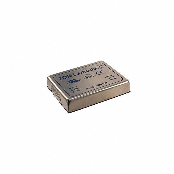
PXE20 Single Output DC/DC Converters
9 to 75 Vdc input, 3.3 to 15 Vdc Single Output, 20W
Features
Low profile: 2.0x1.6x0.4 inches (50.8x40.6x10.2mm)
2:1 wide input voltage of 9-18, 18-36 and 36-75VDC
4:1 ultra wide input voltage of 9-36 and 18-75VDC
20 Watts output power
Input to output isolation: 1600Vdc, min
Operating case temperature range :100℃ max
Over-current protection, auto-recovery
Output over voltage protection
ISO 9001 certified manufacturing facilities
UL60950-1, EN60950-1 and IEC60950-1 licensed
CE Mark meet 2006/95/EC, 93/68/EEC and 2004/108/EC
Compliant to RoHS EU directive 2002/95/EC
Applications
Distributed power architectures
Communications equipment
Computer equipment
General Description
The PXE20 single output series offers 20 Watts of output power from a 2 x 1.6 x 0.4 inch package. The PXE20-xxSxx
models have a 2:1 wide input voltage of 9-18, 18-36 and 36-75VDC. The PXE20-xxWSxx models have a 4:1 wide
input voltage of 9-36 and 18-75VDC.
Table of contents
Absolute Maximum Rating
P2
External trim adjustment
P7
Output Specifications
P2
Characteristic curve
P9
Input Specifications
P3
Test configurations
P26
General Specifications
P3
Part number structure
P27
Thermal Consideration
P4
Mechanical data
P27
Output over current protection
P6
Safety and installation instruction
P28
Short circuit protection
P6
MTBF and Reliability
P28
Solder and Reflow consideration
P7
�Absolute Maximum Rating
Parameter
12Sxx
36
24Sxx
50
48Sxx
100
Unit
Vdc
Vdc
Vdc
+85
℃
100
℃
Device
Input Voltage Continuous Transient (100ms)
Operating temperature range
(Operating temperature will be depended De-rating curve)
Standard
Min
Typ
-40
Operating case range
All
Storage temperature
All
-55
I/O Isolation voltage
All
1600
I/O Isolation capacitance
All
Max
℃
+105
Vdc
300
pF
Output Specifications
Parameter
Device
Min
Typ
Max
xxS33
3.267
3.30
3.333
xxS05
4.95
5.00
5.05
xxS12
11.88
12.00
12.12
xxS15
14.85
15.00
15.15
Line Regulation(LL to HL at Full Load)
All
-0.2
0.2
%
Load Regulation(Min. to 100% Full Load)
All
-0.5
0.5
%
Output Ripple & Noise (20MHz bandwidth)
All
75
mVp-p
Temperature Coefficient
All
+0.02
%/℃
Operating Output Range
Transient Response Recovery Time
(25% load step change)
Output Current
-0.02
All
Unit
Vdc
Vdc
Vdc
μS
250
xxS33
280
4000
mA
xxS05
280
4000
mA
xxS12
134
1670
mA
xxS15
106
1330
mA
xxS33
3.9
Vdc
xxS05
6.2
Vdc
xxS12
15
Vdc
xxS15
18
Vdc
Output Over Current Protection
All
150
% FL.
Output Short Circuit Protection
All
Output Over Voltage Protection Zener diode clamp
Output Capacitor Load
Hiccup, automatics recovery
xxS33
13000
μF
xxS05
6800
μF
xxS12
2200
μF
xxS15
755
μF
2
�Input Specifications
Parameter
Operating Input Voltage
Input reflected ripple current
Start Up Time
(nominal Vin and constant resistive load)
Device
Min
Typ
Max
Unit
12Sxx
9
12
18
Vdc
24(W)Sxx
18(9)
24
36
Vdc
48(W)Sxx
36(18)
48
75
Vdc
All
25
mA p-p
All
20
mS
Remote ON/OFF
Positive Logic
DC-DC ON
All
3.5
12
Vdc
DC-DC OFF
All
0
1.2
Vdc
General Specifications
Parameter
Efficiency
Test at Vin, nom and full load
Device
Min
Typ
Max
Unit
12S3P3
77
%
12S05
80
%
12S12
83
%
12S15
84
%
24(W)S3P3
79(76)
%
24(W)S05
81(79)
%
24(W)S12
86(81)
%
24(W)S15
86(81)
%
48(W)S3P3
79(77)
%
48(W)S05
82(80)
%
48(W)S12
86(82)
%
48(W)S15
86(82)
%
9
Ω
Isolation Resistance
All
Isolation Capacitance
All
Switching Frequency(Test at Vin, nom and full load)
All
300
KHz
All
250
uS
Transient Response Recovery Time
(25% load step change)
10
300
Weight
All
48
MTBF (please see the MTBF and reliability part)
All
1.928×10
pF
g
6
hours
3
�Thermal Consideration
The power module operates in a variety of thermal environments. However, sufficient cooling should be provided to
help ensure reliable operation of the unit. Heat is removed by conduction, convection, and radiation to the surrounding
environment. Proper cooling can be verified by measuring the point shown in the figure below. The temperature at this
location should not exceed 100C. When operating, adequate cooling must be provided to maintain the test point
temperature at or below 100C. Although the maximum point temperature of the power modules is 100C, limiting this
temperature to a lower value will yield higher higher reliability.
De-rating curves for PXE20-12S3P3, PXE20-24S05, PXE20-48S15, PXE20-24WS3P3, and PXE20-48WS12
PXE 20 -1 2S3 P3 De ra tin g C urve
1 20
Ou tpu t Pow e r(% )
1 00
80
60
40
nature convection
nature convection
with heat-sink
20
0
- 40 -3 0 - 20 -1 0
0
10
20
30
40
50
60
70
80
9 0 10 0
70
80
90 1 00
Am bi e nt Temp e ratu re( ℃ )
PXE 20 -2 4S 05 De ra ti ng Cu rve
12 0
Outp ut Po wer(% )
10 0
80
60
40
nature convection
nature convection
with heat-sink
20
0
-4 0 - 30 -2 0 -10
0
10
20
30
40
50
60
Am bi en t Te mp e ratu re( ℃ )
4
�PXE20-48S15 Derating Curve
120
100
Output Power(%)
80
60
40
nature convection
nature convection
with heat-sink
20
0
-40 -30 -20 -10
0
10 20 30 40 50 60 70 80 90 100
Ambient Temperature( ℃)
PXE20-24WS3P3
120
Output Power(%)
100
80
60
nature convection
nature convection
with heat-sink
40
20
0
-40 -30 -20 -10
0
10 20 30 40 50 60
Ambient Temperature( ℃)
70
80
90 100
PXE20- 48WS12
120
100
80
nature convection
nature convection
with heat-sink
60
40
20
0
- 40 - 30 - 20 - 10
0
10
20
30 40 50 60 70 80 90 100
Ambient Temperature( ℃)
5
�Output over current protection
When excessive output currents occur in the system, circuit protection is required on all power supplies.
Normally, overload current is maintained at approximately 150 percent of rated current for the PXE20-S Series.
Hiccup-mode is a method of operation in a power supply whose purpose is to protect the power supply from
being damaged during an over-current fault condition. It also enables the power supply to restart when the fault is
removed. There are other ways of protecting the power supply when it is over-loaded, such as the maximum current
limiting or current foldback methods.
One of the problems resulting from over current is that excessive heat may be generated in power devices;
especially MOSFET and Schottky diodes and the temperature of those devices may exceed their specified limits. A
protection mechanism has to be used to prevent those power devices from being damaged.
The operation of hiccup is as follows. When the current sense circuit sees an over-current event, the controller
shuts off the power supply for a given time and then tries to start up the power supply again. If the over-load condition
has been removed, the power supply will start up and operate normally; otherwise, the controller will see another
over-current event and shut off the power supply again, repeating the previous cycle. Hiccup operation has none of
the drawbacks of the other two protection methods, although its circuit is more complicated because it requires a
timing circuit. The excess heat due to overload lasts for only a short duration in the hiccup cycle, hence the junction
temperature of the power devices is much lower.
The hiccup operation can be done in various ways. For example, one can start hiccup operation any time
an over-current event is detected; or prohibit hiccup during a designated start-up is usually larger than during
normal operation and it is easier for an over-current event is detected; or prohibit hiccup during a designated
start-up interval (usually a few milliseconds). The reason for the latter operation is that during start-up, the power
supply needs to provide extra current to charge up the output capacitor. Thus the current demand during start-up
is usually larger than during normal operation and it is easier for an over-current event to occur. If the power
supply starts to hiccup once there is an over-current, it might never start up successfully. Hiccup mode protection
will give the best protection for a power supply against over current situations, since it will limit the average current
to the load at a low level, so reducing power dissipation and case temperature in the power devices.
Short Circuit Protection
Continuous, hiccup and auto-recovery mode.
6
�Soldering and Reflow Consideration
Lead free wave solder profile for PXE20-S DIP type
Zone
Reference Parameter
Preheat zone
Rise temp. speed : 3℃/ sec max.
Preheat temp. : 100~130℃
Actual heating
Peak temp. : 250~260℃
Peak time (T1+T2 time) : 4~6 sec
Reference Solder:Sn-Ag-Cu;Sn-Cu
Hand Welding:Soldering iron:Power 90W
Welding Time:2~4 sec
Temp.:380~400 ℃
External trim adjustment
Output voltage set point adjustment allows the user to increase or decrease the output voltage set point of a module. This is
accomplished by connecting an external resistor between the TRIM pin and either the Vo (+) or Vo (-) pins. With an external resistor
between the TRIM and Vo (+) pin, the output voltage set point decreases. With an external resistor between the TRIM and Vo (-) pin,
the output voltage set point increases.
1
+Output♁
6
-Output♁
7
♁ +Input
Trim down
Rd
♁ -Input
2
Trim
♁
8
7
�+Output♁
1
6
♁ +Input
-Output♁
7
♁ -Input
.
Trim up
2
Trim
Ru
♁
8
EXTERNAL OUTPUT TRIMMING
TRIM TABLE
PXE20-xxS3P3
Trim down
1
2
3
4
5
6
7
8
9
10
%
Vout=
3.266
3.233
3.200
3.167
3.134
3.101
3.068
3.035
3.002
2.969
Volts
Rx=
69.470
31.235
18.490
12.117
8.294
5.745
3.924
2.559
1.497
0.647
K Ohms
Trim up
1
2
3
4
5
6
7
8
9
10
%
Vout=
3.332
3.365
3.398
3.431
3.464
3.497
3.530
3.563
3.596
3.629
Volts
Rx=
57.930
26.165
15.577
10.283
7.106
4.988
3.476
2.341
1.459
0.753
K Ohms
Trim down
1
2
3
4
5
6
7
8
9
10
%
Vout=
4.952
4.902
4.852
4.802
4.752
4.702
4.652
4.602
4.552
4.502
Volts
0.676 K Ohms
PXE20-xxS05
Rx=
45.533
20.612
12.306
8.152
5.660
3.999
2.812
1.922
1.230
Trim up
1
2
3
4
5
6
7
8
9
10
%
Vout=
5.052
5.102
5.152
5.202
5.252
5.302
5.352
5.402
5.452
5.502
Volts
Rx=
36.570
16.580
9.917
6.585
4.586
3.253
2.302
1.588
1.032
0.588 K Ohms
7
8
9
PXE20-xxS12
Trim down
1
2
3
Vout=
11.887
11.767
11.647
Rx=
4
5
6
10
11.527 11.407 11.287 11.166 11.046 10.926 10.806
460.659 207.779 123.486 81.340 56.052 39.193 27.151 18.120 11.095
5
6
7
8
9
1
2
3
Vout=
12.127
12.247
12.367
12.487 12.607 12.727 12.847 12.967 13.088 13.208
368.241 166.121
98.747
65.060 44.848 31.374 21.749 14.530
8.916
Volts
5.476 K Ohms
Trim up
Rx=
4
%
10
%
Volts
4.424 K Ohms
PXE20-xxS15
Trim down
1
2
3
Vout=
14.808
14.658
14.509
Rx=
5
6
7
8
1
2
3
Vout=
15.107
15.256
15.406
9
10
14.359 14.209 14.060 13.910 13.761 13.611 13.462
499.816 223.408 131.272 85.204 57.563 39.136 25.974 16.102
Trim up
Rx=
4
4
5
6
7
8
8.424
9
6.687
Volts
2.282 K Ohms
10
15.556 15.705 15.855 16.004 16.154 16.304 16.453
404.184 180.592 106.061 68.796 46.437 31.531 20.883 12.898
%
%
Volts
1.718 K Ohms
8
�Characteristic Curve
Efficiency
a. Efficiency with load change under different line condition at room temperature
PXE20-12S3P3
85.00
80.00
Eff(%)
75.00
9V
12V
18V
70.00
65.00
60.00
0.4 0.8 1.2 1.6
2
2.4 2.8 3.2 3.6
4
lout(A )
PXE20-24S05
90.00
Eff(%)
85.00
80.00
75.00
18V
24V
36V
70.00
65.00
0.4 0.8 1.2 1.6
2
2.4 2.8 3.2 3.6
4
lout(A )
PXE20- 48S15
90.00
85.00
Eff(%)
80.00
75.00
36V
48V
75V
70.00
65.00
60.00
133 266 399
532 665 798
931 1064 1197 1330
lout(mA )
9
�P XE20-24WS3P 3
85.00
80.00
75.00
70.00
65.00
9V
24V
36V
60.00
55.00
50.00
400 800 1200 1600 2000 2400 2800 3200 3600 4000
lo ut(mA )
PXE20-48WS12
90.00
85.00
Eff(%)
80.00
75.00
70.00
18V
48V
75V
65.00
60.00
55.00
167
334
501
668
835 1002 1169 1336 1503 1670
lout(mA )
10
�b. Efficiency with line change under different load condition at room temperature
PXE20-12S3P3
85.00
Eff(%)
80.00
75.00
4000mA
2000mA
400mA
70.00
65.00
60.00
9V 10V 11V 12V 13V 14V 15V 16V 17V 18V
Vin(V)
PXE20-24S05
90.00
Eff(%)
85.00
80.00
75.00
4000mA
2000mA
400mA
70.00
65.00
18V 20V 22V 24V 26V 28V 30V 32V 34V 36V
Vin(V)
PXE20-48S15
90.00
85.00
Eff(%)
80.00
75.00
70.00
1330mA
665mA
133mA
65.00
60.00
36V 40V 44V 48V 52V 56V 60V 64V 68V 75V
Vin(V)
11
�PXE20-24WS3P3
90.00
80.00
4000mA
2000mA
400mA
Eff(%)
70.00
60.00
50.00
40.00
30.00
9V
12V 15V 18V 21V 24V 27V 30V 33V 36V
Vin(V)
PXE20-48WS12
90.00
85.00
Eff(%)
80.00
75.00
4000mA
2000mA
400mA
70.00
65.00
60.00
55.00
18V 24V 30V 36V 42V 48V 54V 60V 66V 75V
Vin(V)
12
�c. Power Dissipation Curves
PXE20-12S3P3
5.000
pd(w)
4.000
9V
12V
18V
3.000
2.000
1.000
0.000
0.4 0.8 1.2 1.6
2
2.4 2.8 3.2 3.6
4
lout(A )
PXE20-24S05
5.000
pd(w)
4.000
18V
24V
36V
3.000
2.000
1.000
0.000
0.4 0.8 1.2 1.6
2
2.4 2.8 3.2 3.6
4
lout(A )
PXE20-48S15
4.500
pd(w)
3.500
2.500
36V
48V
75V
1.500
0.500
0.13 0.26 0.39 0.52 0.65 0.78 0.91 1.04 1.17 1.33
lout(A )
13
�PXE20-24WS3P3
4.500
18V
24V
36V
pd(w)
3.500
2.500
1.500
0.500
400
800 1200 1600 2000 2400 2800 3200 3600 4000
lout(mA )
PXE20-48WS12
4.000
pd(w)
3.000
2.000
1.000
36V
48V
75V
0.000
167
334
501
668
835 1002 1169 1336 1503 1670
lout(mA )
14
�Output ripple & noise
PXE20-12S3P3
Low Line, Full Load
Normal Line, Full Load
High Line, Full Load
Ripple noise=10.0mV
Ripple noise=10.8mV
Ripple noise=12.4mV
PXE20-24S05
Low Line, Full Load
Normal Line, Full Load
High Line, Full Load
Ripple noise=11.2mV
Ripple noise=13.6mV
Ripple noise=18.4mV
PXE20-48S15
Low Line, Full Load
Normal Line, Full Load
High Line, Full Load
Ripple noise=19.2mV
Ripple noise=22.4mV
Ripple noise=35.2mV
15
�PXE20-24WS3P3
Low Line, Full Load
Normal Line, Full Load
High Line, Full Load
Ripple noise=23.2mV
Ripple noise=31.5mV
Ripple noise=30.4mV
PXE20-48WS12
Low Line, Full Load
Normal Line, Full Load
High Line, Full Load
Ripple noise=38.5mV
Ripple noise=67.6mV
Ripple noise=98.4mV
16
�Transient Peak and Response
PXE20-12S3P3
Low Line, Full Load
Normal Line, Full Load
High Line, Full Load
Transient Peak 83.0mV
Transient Peak 87.0mV
Transient Peak 91.0mV
Transient Response 102uS
Transient Response 102uS
Transient Response 106uS
PXE20-24S05
Low Line, Full Load
Normal Line, Full Load
High Line, Full Load
Transient Peak 103mV
Transient Peak 106mV
Transient Peak 106mV
Transient Response 80uS
Transient Response 86uS
Transient Response 96uS
PXE20-48S15
Low Line, Full Load
Normal Line, Full Load
High Line, Full Load
Transient Peak 113mV
Transient Peak 114mV
Transient Peak 113mV
Transient Response 100uS
Transient Response 100uS
Transient Response 106uS
17
�PXE20-24WS3P3
Low Line, Full Load
Normal Line, Full Load
High Line, Full Load
Transient Peak 110mV
Transient Peak 115mV
Transient Peak 125mV
Transient Response 90Us
Transient Response 86uS
Transient Response 190uS
PXE20-48WS12
Low Line, Full Load
Normal Line, Full Load
High Line, Full Load
Transient Peak 182mV
Transient Peak 204mV
Transient Peak 232mV
Transient Response 130uS
Transient Response 164uS
Transient Response 154uS
18
�Inrush Current
PXE20-12S3P3
Low Line, Full Load
Normal Line, Full Load
High Line, Full Load
Inrush current=(61.2/10) X500mA=3060mA
Inrush current=(38.2/10) x500mA=1910mA
Inrush current=(26.2/10) x500mA=1310mA
Low Line, Full Load
Normal Line, Full Load
High Line, Full Load
Duration: 304uS
Duration: 288uS
Duration: 240uS
PXE20-24S05
Low Line, Full Load
Normal Line, Full Load
High Line, Full Load
Inrush current=(31.6/10) X500mA=1580mA
Inrush current=(23.8/10) x500mA=1190mA
Inrush current=(15.0/10) x500mA=750mA
Low Line, Full Load
Normal Line, Full Load
High Line, Full Load
Duration: 336uS
Duration: 304uS
Duration: 328uS
19
�PXE20-48S15
Low Line, Full Load
Normal Line, Full Load
High Line, Full Load
Inrush current=(41.0/10) X200mA=820mA
Inrush current=(31.0/10) x200mA=620mA
Inrush current=(21.6/10) x200mA=432mA
Low Line, Full Load
Normal Line, Full Load
High Line, Full Load
Duration: 600uS
Duration: 540uS
Duration: 520uS
PXE20-24WS3P3
Low Line, Full Load
Normal Line, Full Load
High Line, Full Load
Inrush current=(42.8/10) X500mA=2140mA
Inrush current=(18.4/10) x500mA=920mA
Inrush current=(13.8/10) x500mA=690mA
Low Line, Full Load
Normal Line, Full Load
High Line, Full Load
Duration: 240uS
Duration: 180uS
Duration: 160uS
20
�PXE20-48WS12
Low Line, Full Load
Normal Line, Full Load
High Line, Full Load
Inrush current=(23.4/10) X500mA=1170mA
Inrush current=(10/10) x500mA=500mA
Inrush current=(1010) x500mA=500mA
Low Line, Full Load
Normal Line, Full Load
High Line, Full Load
Duration: 0uS
Duration: 200uS
Duration: 140uS
21
�Input Ripple Current
PXE20-12S3P3
Low Line, Full Load
Normal Line, Full Load
High Line, Full Load
Ripple current=(4.2/10) x20=8.4mA
Ripple current=(3.2/10) x20=6.4mA
Ripple current=(2.8/10) x20=5.6mA
PXE20-24S05
Low Line, Full Load
Normal Line, Full Load
High Line, Full Load
Ripple current=(2.41/10) x20=4.82mA
Ripple current=(2.61/10) x20=5.22mA
Ripple current=(2.79/10) x20=5.58mA
PXE20-48S15
Low Line, Full Load
Normal Line, Full Load
High Line, Full Load
Ripple current=(3.0/10) x20=6mA
Ripple current=(3.4/10) x20=6.8mA
Ripple current=(3.8/10) x20=7.6mA
22
�PXE20-24WS3P3
Low Line, Full Load
Normal Line, Full Load
High Line, Full Load
Ripple current=(4.6/10) x10=4.6mA
Ripple current=(3.0/10) x10=3.0mA
Ripple current=(3.2/10) x10=3.2mA
PXE20-48WS12
Low Line, Full Load
Normal Line, Full Load
High Line, Full Load
Ripple current=(3.4/10) x10=3.4mA
Ripple current=(3..2/10) x10=3.2mA
Ripple current=(3.6/10) x10=3.6mA
23
�Delay Time and Raise Time
PXE20-12S3P3
Normal Line, Full Load
Normal Line, Full Load
Rise Time=397.0uS
Delay Time= 624uS
PXE20-24S05
Normal Line, Full Load
Normal Line, Full Load
Rise Time=272.5uS
Delay Time= 500uS
PXE20-48S15
Normal Line, Full Load
Normal Line, Full Load
Rise Time=696.7uS
DelayTime=1.16mS
24
�PXE20-24WS3P3
Normal Line, Full Load
Normal Line, Full Load
Rise Time=480uS
DelayTime=620uS
PXE20-48WS12
Normal Line, Full Load
Normal Line, Full Load
Rise Time=5.12mS
DelayTime=5.36mS
25
�Testing Configurations
Input reflected-ripple current Measurement:
Component
L
C
Value
12μH
220μF
Voltage
---100V
Reference
---Aluminum Electrolytic Capacitor
Peak-to-peak output ripple & noise Measurement:
Output Voltage and Efficiency Measurement:
Note: All measurements are taken at the module terminals.
V Io
100%
Efficiency o
Vin I in
26
�Part Number Structure
PXE 20 – 24 (W)S 12
Total Output power
20 Watt
Input Voltage Range
12xxx : 9~18V
24xxx : 18~36V
48xxx : 36~75V
24Wxxx: 9~36V
48Wxxx: 18~75V
4:1 Wide Input
Voltage Range
Output Voltage
3P3 : 3.3V
05 : 5V
12 : 12V
15 : 15V
Single
Output
Mechanical Data
Pin
1
2
4
5
6
7
8
PIN CONNECTION
Function
+INPUT
-INPUT
CTRL
NO PIN
+OUTPUT
-OUTPUT
TRIM
EXTERNAL OUTPUT TRIMMING
Output can be externally trimmed by
using the method shown below.
TRIM UP
TRIM DOWN
7
8
RU
8
RD
6
27
�Safety and Installation Instruction
Isolation consideration
The PXE20 series features 1.6k Volt DC isolation from input to output, input to case, and output to case. The input to
9
output resistance is greater than 10 ohms. Nevertheless, if the system using the power module needs safety agency
approval, certain rules must be followed in the design of the system when using the product In particular, all of the
creepage and clearance requirements of the end-use safety requirement must be observed. These documents
include UL-60950-1, EN60950-1 and CSA 22.2-960, although specific applications may have other or additional
requirements.
Fusing Consideration
Caution: This power module is not internally fused. An input line fuse must always be used. This encapsulated power
module can be used in a wide variety of applications, ranging from simple stand-alone operation to an integrated part
of a sophisticated power architecture. To maximum flexibility, internal fusing is not included; however, to achieve
maximum safety and system protection, always use an input line fuse. The safety agencies require a slow-blow fuse
with maximum rating of 6.3 A. Based on the information provided in this data sheet on inrush energy and maximum
dc input current, the same type of fuse with lower rating can be used. Refer to the fuse manufacturer’s data for further
information.
Minimum Load Requirement
10%(of full load) minimum load required. The 10% minimum load requirement is in order to meet all performance
specifications. The PXE20 Series does not properly maintain regulation and operate with a no load condition. The
output voltage drops off about 10%.
MTBF and Reliability
The MTBF of PXE20- has been calculated using:
1.MIL-HDBK-217F under the following conditions:
Nominal Input Voltage
Io = Io, max
Ta = 25℃
5
The resulting figure for MTBF is 7.650× 10 hours.
2.Bell-core TR-NWT-000332 Case I:
50% stress, Operating Temperature at 40 ℃ (Ground fixed and controlled environment)
6
The resulting figure for MTBF is 1.928× 10 hours.
28
�


 工商网监
湘ICP备2023018690号
工商网监
湘ICP备2023018690号
