PXE30-xxDxx Dual Output DC/DC Converter
9 to 18 Vdc , 18 to 36 Vdc , or 36 to 75 Vdc input, 12 to 15 Vdc Dual Output, 30W
Features
• 30 watts maximum output power
• Output current up to 1250mA
• Standard 2” x 1.6” x 0.4” package
• High efficiency up to 88%
• 2:1 wide input voltage range
• Six-sided continuous shield
• Fixed switching frequency
• CE MARK meets 2006/95/EC, 93/68/EEC and 2004/108/EC
• UL60950-1, EN60950-1 and IEC60950-1 licensed
• ISO9001 certified manufacturing facilities
• Compliant to RoHS EU directive 2002/95/EC
Options
• Heat sinks available for extended operation
APPLICATIONS
Wireless Network
Telecom/Datacom
Industry Control System
Measurement Equipment
Semiconductor Equipment
General Description
The PXE30-xxDxx series offers 30 watts of output power in a 2 x 1.6 x 0.4 inch package . This series has a
2:1 wide input voltage of 9-18VDC, 18-36VDC or 36-75VDC and features 1600VDC of isolation,
short-circuit and over-voltage protection.
Table of Contents
Absolute Maximum Rating
Output Specification
Input Specification
General Specification
Characteristic Curves
Test Configurations
EMC Considerations
Input Source Impedance
Output Over Current Protection
Output Over Voltage Protection
Short Circuit Protection
Thermal Consideration
P2
P2
P3
P4
P5
P17
P18
P20
P20
P21
P21
P21
Heat Sink Consideration
Remote ON/OFF Control
Mechanical Data
Recommended Pad Layout
Output Voltage Adjustment
Soldering and Reflow Consideration
Packaging Information
Part Number Structure
Safety and Installation Instruction
MTBF and Reliability
P22
P23
P24
P25
P26
P27
P27
P28
P28
P28
�Jun. 20, 2011
30W, Dual Output
Absolute Maximum Rating
Parameter
Model
Input Voltage
Continuous
Transient (100mS)
Input Voltage Variation
(complies with EST300 132 part 4.4)
Operating Ambient Temperature (with derating)
Operating Case Temperature
Storage Temperature
Min
Max
Unit
12Dxx
24Dxx
48Dxx
12Dxx
24Dxx
48Dxx
18
36
75
36
50
100
All
5
V/mS
85
100
105
°C
°C
°C
All
All
All
-40
-55
VDC
Output Specification
Parameter
Output Voltage
(Vin = Vin(nom) ; Full Load ; TA=25°C)
Voltage Adjustability
Min
Typ
Max
xxD12
Model
11.88
12
12.12
xxD15
14.85
15
15.15
Unit
VDC
All
-10
+10
%
All
-0.5
+0.5
%
-1
+1
Output Regulation
Line (Vin(min) to Vin(max) at Full Load)
Load (Min. to 100% of Full Load)
Output Ripple & Noise
Peak-to-Peak (20MHz bandwidth)
xxD12
100
(Measured with a 0.1μF/50V MLCC)
xxD15
100
Temperature Coefficient
Output Voltage Overshoot
(Vin(min) to Vin(max) ; Full Load ; TA=25°C)
All
-0.02
mVp-p
+0.02
%/°C
5
% VOUT
All
0
All
250
mV
All
300
μS
Dynamic Load Response
(Vin = Vin(nom) ; TA=25°C)
Load step change from
75% to 100% or 100 to 75% of Full Load
Peak Deviation
Setting Time (VOUT<10% peak deviation)
Output Current
Output Over Voltage Protection
(Zener diode clamp)
xxD12
0
±1250
xxD15
0
±1000
xxD12
15
xxD15
18
Output Over Current Protection
All
Output Short Circuit Protection
All
mA
VDC
150
% FL.
Hiccup, automatic recovery
VER:00 Page 2 of 28
Issued Date:2009/03/02
�Jun. 20, 2011
30W, Dual Output
Input Specification
Parameter
Operating Input Voltage
Input Current
(Maximum value at Vin = Vin(nom); Full Load)
Model
Min
Typ
Max
12Dxx
9
12
18
24Dxx
18
24
36
48Dxx
36
48
Input Standby Current
(Typical value at Vin = Vin(nom); No Load)
Under Voltage Lockout Turn-on Threshold
Under Voltage Lockout Turn-off Threshold
Input Reflected Ripple Current
(5 to 20MHz, 12μH Source Impedance)
VDC
75
12D12
3012
12D15
3012
24D12
1488
24D15
1488
48D12
744
48D15
Unit
mA
744
12D12
60
12D15
40
24D12
30
24D15
30
48D12
20
48D15
20
mA
12Dxx
9
24Dxx
17.8
48Dxx
36
12Dxx
8
24Dxx
16
48Dxx
33
All
30
VDC
VDC
mAp-p
Start Up Time
(Vin = Vin(nom) and Constant Resistive Load)
Power Up
All
25
Remote ON/OFF
mS
25
Remote ON/OFF Control
(The ON/OFF pin voltage is referenced to -VIN)
Positive Logic
DC-DC ON
All
DC-DC OFF
Remote Off Input Current
All
Input Current of Remote Control Pin
All
3.0
12
0
1.2
2.5
-0.5
VER:00 Page 3 of 28
VDC
mA
0.5
mA
Issued Date:2009/03/02
�Jun. 20, 2011
30W, Dual Output
General Specification
Parameter
Efficiency
(Vin = Vin(nom) ; Full Load ; TA=25°C)
Model
Min
Typ
12D12
87
12D15
87
24D12
88
24D15
88
48D12
88
48D15
88
Max
Unit
%
Isolation Voltage
Input to Output
All
Input to Case, Output to Case
1600
VDC
1600
GΩ
Isolation Resistance
All
1
Isolation Capacitance
All
Switching Frequency
All
300
kHz
Weight
All
48
g
All
1.316×10⁶
3.465×10⁵
hours
All
115
°C
1000
pF
MTBF
Bellcore TR-NWT-000332, TC=40°C
MIL-HDBK-217F
Over Temperature Protection
VER:00 Page 4 of 28
Issued Date:2009/03/02
�Jun. 20, 2011
30W, Dual Output
Characteristic Curves
All test conditions are at 25°C.The figures are or PXE30-12D12
Efficiency Versus Output Current
Efficiency Versus Input Voltage. Full Load
Power Dissipation Versus Output Current
Derating Output Current Versus Ambient Temperature and
Airflow Vin=Vin(nom)
Derating Output Current Versus Ambient Temperature with Heat-Sink
and Airflow, Vin = Vin(nom)
VER:00 Page 5 of 28
Issued Date:2009/03/02
�Jun. 20, 2011
30W, Dual Output
Characteristic Curves (Continued)
All test conditions are at 25°C.The figures are for PXE30-12D12
Typical Output Ripple and Noise.
Transient Response to Dynamic Load Change from
Vin=Vin(nom), Full Load
100% to 75% to 100% of Full Load ; Vin=Vin(nom)
Typical Input Start-Up and Output Rise Characteristic
Using ON/OFF Voltage Start-Up and Vo Rise Characteristic
Vin=Vin(nom), Full Load
Vin=Vin(nom), Full Load
Conduction Emission of EN55022 Class A
Conduction Emission of EN55022 Class B
Vin=Vin(nom), Full Load
Vin=Vin(nom), Full Load
VER:00 Page 6 of 28
Issued Date:2009/03/02
�Jun. 20, 2011
30W, Dual Output
Characteristic Curves (Continued)
All test conditions are at 25°C.The figures are for PXE30-12D15
Efficiency Versus Output Current
Efficiency Versus Input Voltage. Full Load
Power Dissipation Versus Output Current
Derating Output Current Versus Ambient Temperature and
Airflow Vin=Vin(nom)
Derating Output Current Versus Ambient Temperature with Heat-Sink
and Airflow, Vin = Vin(nom)
VER:00 Page 7 of 28
Issued Date:2009/03/02
�Jun. 20, 2011
30W, Dual Output
Characteristic Curves (Continued)
All test conditions are at 25°C.The figures are for PXE30-12D15
Typical Output Ripple and Noise.
Transient Response to Dynamic Load Change from
Vin=Vin(nom), Full Load
100% to 75% to 100% of Full Load ; Vin=Vin(nom)
Typical Input Start-Up and Output Rise Characteristic
Using ON/OFF Voltage Start-Up and Vo Rise Characteristic
Vin=Vin(nom), Full Load
Vin=Vin(nom), Full Load
Conduction Emission of EN55022 Class A
Conduction Emission of EN55022 Class B
Vin=Vin(nom), Full Load
Vin=Vin(nom), Full Load
VER:00 Page 8 of 28
Issued Date:2009/03/02
�Jun. 20, 2011
30W, Dual Output
Characteristic Curves (Continued)
All test conditions are at 25°C.The figures are for PXE30-24D12
Efficiency Versus Output Current
Efficiency Versus Input Voltage. Full Load
Power Dissipation Versus Output Current
Derating Output Current Versus Ambient Temperature and
Airflow Vin=Vin(nom)
Derating Output Current Versus Ambient Temperature with Heat-Sink
and Airflow, Vin = Vin(nom)
VER:00 Page 9 of 28
Issued Date:2009/03/02
�Jun. 20, 2011
30W, Dual Output
Characteristic Curves (Continued)
All test conditions are at 25°C.The figures are for PXE30-24D12
Typical Output Ripple and Noise.
Transient Response to Dynamic Load Change from
Vin=Vin(nom), Full Load
100% to 75% to 100% of Full Load ; Vin=Vin(nom)
Typical Input Start-Up and Output Rise Characteristic
Using ON/OFF Voltage Start-Up and Vo Rise Characteristic
Vin=Vin(nom), Full Load
Vin=Vin(nom), Full Load
Conduction Emission of EN55022 Class A
Conduction Emission of EN55022 Class B
Vin=Vin(nom), Full Load
Vin=Vin(nom), Full Load
VER:00 Page 10 of 28 Issued Date:2009/03/02
�Jun. 20, 2011
30W, Dual Output
Characteristic Curves (Continued)
All test conditions are at 25°C.The figures are for PXE30-24D15
Efficiency Versus Output Current
Efficiency Versus Input Voltage. Full Load
Power Dissipation Versus Output Current
Derating Output Current Versus Ambient Temperature and
Airflow Vin=Vin(nom)
Derating Output Current Versus Ambient Temperature with Heat-Sink
and Airflow, Vin = Vin(nom)
VER:00 Page 11 of 28 Issued Date:2009/03/02
�Jun. 20, 2011
30W, Dual Output
Characteristic Curves (Continued)
All test conditions are at 25°C.The figures are for PXE30-24D15
Typical Output Ripple and Noise.
Transient Response to Dynamic Load Change from
Vin=Vin(nom), Full Load
100% to 75% to 100% of Full Load ; Vin=Vin(nom)
Typical Input Start-Up and Output Rise Characteristic
Using ON/OFF Voltage Start-Up and Vo Rise Characteristic
Vin=Vin(nom), Full Load
Vin=Vin(nom), Full Load
Conduction Emission of EN55022 Class A
Conduction Emission of EN55022 Class B
Vin=Vin(nom), Full Load
Vin=Vin(nom), Full Load
VER:00 Page 12 of 28 Issued Date:2009/03/02
�Jun. 20, 2011
30W, Dual Output
Characteristic Curves (Continued)
All test conditions are at 25°C.The figures are for PXE30-48D12
Efficiency Versus Output Current
Efficiency Versus Input Voltage. Full Load
Power Dissipation Versus Output Current
Derating Output Current Versus Ambient Temperature and
Airflow Vin=Vin(nom)
Derating Output Current Versus Ambient Temperature with Heat-Sink
and Airflow, Vin = Vin(nom)
VER:00 Page 13 of 28 Issued Date:2009/03/02
�Jun. 20, 2011
30W, Dual Output
Characteristic Curves (Continued)
All test conditions are at 25°C.The figures are for PXE30-48D12
Typical Output Ripple and Noise.
Transient Response to Dynamic Load Change from
Vin=Vin(nom), Full Load
100% to 75% to 100% of Full Load ; Vin=Vin(nom)
Typical Input Start-Up and Output Rise Characteristic
Using ON/OFF Voltage Start-Up and Vo Rise Characteristic
Vin=Vin(nom), Full Load
Vin=Vin(nom), Full Load
Conduction Emission of EN55022 Class A
Conduction Emission of EN55022 Class B
Vin=Vin(nom), Full Load
Vin=Vin(nom), Full Load
VER:00 Page 14 of 28 Issued Date:2009/03/02
�Jun. 20, 2011
30W, Dual Output
Characteristic Curves (Continued)
All test conditions are at 25°C.The figures are for PXE30-48D15
Efficiency Versus Output Current
Efficiency Versus Input Voltage. Full Load
Power Dissipation Versus Output Current
Derating Output Current Versus Ambient Temperature and
Airflow Vin=Vin(nom)
Derating Output Current Versus Ambient Temperature with Heat-Sink
and Airflow, Vin = Vin(nom)
VER:00 Page 15 of 28 Issued Date:2009/03/02
�Jun. 20, 2011
30W, Dual Output
Characteristic Curves (Continued)
All test conditions are at 25°C.The figures are for PXE30-48D15
Typical Output Ripple and Noise.
Transient Response to Dynamic Load Change from
Vin=Vin(nom), Full Load
100% to 75% to 100% of Full Load ; Vin=Vin(nom)
Typical Input Start-Up and Output Rise Characteristic
Using ON/OFF Voltage Start-Up and Vo Rise Characteristic
Vin=Vin(nom), Full Load
Vin=Vin(nom), Full Load
Conduction Emission of EN55022 Class A
Conduction Emission of EN55022 Class B
Vin=Vin(nom), Full Load
Vin=Vin(nom), Full Load
VER:00 Page 16 of 28 Issued Date:2009/03/02
�Jun. 20, 2011
30W, Dual Output
Test Configurations
Input reflected-ripple current measurement test:
Component
L
C
Value
12μH
220μF
Voltage
---100V
Reference
---Aluminum Electrolytic Capacitor
Peak-to-peak output ripple & noise measurement test:
Output voltage and efficiency measurement test:
Note: All measurements are taken at the module terminals.
V × Io
× 100%
Efficiency = o
Vin × I in
VER:00 Page 17 of 28 Issued Date:2009/03/02
�Jun. 20, 2011
30W, Dual Output
EMC Considerations
Suggested Schematic for EN55022 Conducted Emission Class A Limits
Recommended Layout with Input Filter
To meet conducted emissions EN 55022 CLASS A the following components are needed:
PXE30-12Dxx
Component
C1
C3、C4
Value
6.8μF
1000pF
Voltage
50V
2KV
1812 MLCC
1808 MLCC
PXE30-24Dxx
Component
C1
C3:C4
Value
6.8μF
1000pF
Voltage
50V
2KV
1812 MLCC
1808 MLCC
PXE30-48Dxx
Component
C1
C3:C4
Value
2.2μF
1000pF
Voltage
100V
2KV
1812 MLCC
1808 MLCC
Reference
Reference
Reference
VER:00 Page 18 of 28 Issued Date:2009/03/02
�Jun. 20, 2011
30W, Dual Output
EMC Considerations (Continued)
Suggested Schematic for EN55022 Conducted Emission Class B Limits
Recommended Layout with Input Filter
To meet conducted emissions EN55022 CLASS B needed the following components:
PXE30-12Dxx
Component
C1:C3
C5:C6
L1
Value
4.7μF
1000pF
450μH
Voltage
50V
2KV
----
Reference
1812 MLCC
1808 MLCC
Common Choke
PXE30-24Dxx
Component
C1:C3
C5:C6
L1
Value
6.8μF
1000pF
450μH
Voltage
50V
2KV
----
Reference
1812 MLCC
1808 MLCC
Common Choke
PXE30-48Dxx
Component
C1:C2
C3:C4
C5:C6
L1
Value
2.2μF
2.2μF
1000pF
450μH
Voltage
100V
100V
2KV
----
Reference
1812 MLCC
1812 MLCC
1808 MLCC
Common Choke
VER:00 Page 19 of 28 Issued Date:2009/03/02
�Jun. 20, 2011
30W, Dual Output
EMC Considerations (Continued)
This Common Choke L1 is defined as follows:
■
L:450μH±35% / DCR:25mΩ, max
A height:9.8 mm, Max
■ All dimensions in millimeters
Input Source Impedance
The power module should be connected to a low impedance input source. Highly inductive source impedance
can affect the stability of the power module. Input external L-C filter is recommended to minimize input reflected ripple
current. The inductor has a simulated source impedance of 12μH and capacitor is Nippon chemi-con KY series
220μF/100V. The capacitor must as close as possible to the input terminals of the power module for lower impedance.
Output Over Current Protection
When excessive output currents occur in the system, circuit protection is required on all converters. Normally,
overload current is maintained at approximately 150 percent of rated current for PXF40-xxSxx series.
Hiccup-mode is a method of operation in a converter whose purpose is to protect the power supply from being
damaged during an over-current fault condition. It also enables the converter to restart when the fault is removed.
There are other ways of protecting the converter when it is over-loaded, such as the maximum current limiting or
current foldback methods.
One of the problems resulting from over current is that excessive heat may be generated in power devices;
especially MOSFET and Schottky diodes and the temperature of these devices may exceed their specified limits. A
protection mechanism has to be used to prevent these power devices from being damaged.
The operation of hiccup is as follows. When the current sense circuit sees an over-current event, the controller
shuts off the converter for a given time and then tries to start up the converter again. If the over-load condition has
been removed, the converter will start up and operate normally; otherwise, the controller will see another over-current
event and will shut off the converter again, repeating the previous cycle. Hiccup operation has none of the drawbacks
of the other two protection methods, although its circuit is more complicated because it requires a timing circuit. The
excess heat due to overload lasts for only a short duration in the hiccup cycle, hence the junction temperature of the
power devices is much lower.
VER:00 Page 20 of 28 Issued Date:2009/03/02
�Jun. 20, 2011
30W, Dual Output
Output Over Voltage Protection
The output over-voltage protection consists of a Zener diode that monitors the voltage on the output terminals. If
the voltage on the output terminals exceeds the over-voltage protection threshold, then the Zener diode clamps the
output voltage.
Short Circuit Protection
Continuous, hiccup and auto-recovery mode.
During a short circuit, the converter shut s down. The average current during this condition will be very low .
Thermal Consideration
The power module operates in a variety of thermal environments. However, sufficient cooling should be provided
to help ensure reliable operation of the unit. Heat is removed by conduction, convection, and radiation to the
surrounding environment. Proper cooling can be verified by measuring the point as shown in the figure below. The
temperature at this location should not exceed 100°C. When operating, adequate cooling must be provided to
maintain the test point temperature at or below 100°C. Although the maximum point temperature of the power
modules is 100°C, limiting this temperature to a lower value will yield higher reliability.
VER:00 Page 21 of 28 Issued Date:2009/03/02
�Jun. 20, 2011
30W, Dual Output
Heat Sink Consideration
Optional heat-sink (HAPXE) and optional heat sink clip (HAPXECLIP); two clips required when used.
All dimensions in millimeters
VER:00 Page 22 of 28 Issued Date:2009/03/02
�Jun. 20, 2011
30W, Dual Output
Remote ON/OFF Control
The Remote ON/OFF Pin is used to turn on and off the DC/DC power module. The user must use a switch to
control the logic voltage (high or low level ) of the pin referenced to -Vin. The switch can be an open collector transistor,
FET and Opto-Coupler. The switch must be capable of sinking up to 0.5 mA at low-level logic voltage. High-level logic
of the ON/OFF signal (maximum voltage): the allowable leakage current of the switch at 12V is 0.5mA.
Remote ON/OFF Implementation Circuits
Isolated-Clontrol Remote ON/OFF
Level Control Using TTL Output
Level Control Using Line Voltage
Positive Logic:
When PXE30 module is turned off
When PXE30 module is turned on
at Low-level logic
at High-level logic
VER:00 Page 23 of 28 Issued Date:2009/03/02
�Jun. 20, 2011
30W, Dual Output
Mechanical Data
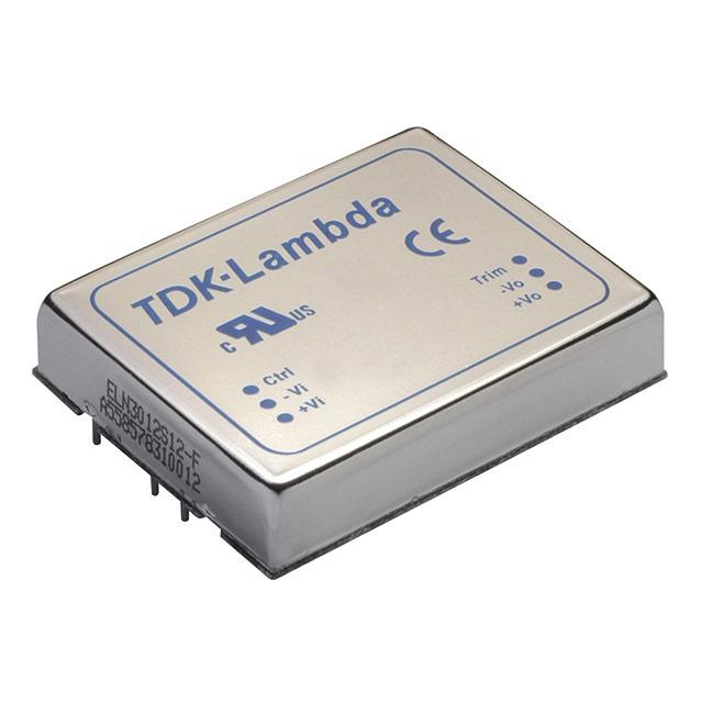
PIN
1
2
4
5
6
7
8
PIN CONNECTION
FUNCTION
+INPUT
-INPUT
CTRL
+OUTPUT
COMMON
-OUTPUT
TRIM
EXTERNAL OUTPUT TRIMMING
Output can be externally trimmed by
using the method shown below.
TRIM UP
TRIM DOWN
7
8
RU
8
RD
5
VER:00 Page 24 of 28 Issued Date:2009/03/02
�Jun. 20, 2011
30W, Dual Output
Recommended Pad Layout
VER:00 Page 25 of 28 Issued Date:2009/03/02
�Jun. 20, 2011
30W, Dual Output
Output Voltage Adjustment
Output voltage set point adjustment allows the user to increase or decrease the output voltage set point of a
module. This is accomplished by connecting an external resistor between the TRIM pin and either the Vo(+) or Vo(-)
pins. With an external resistor between the TRIM and Vo(-) pin, the output voltage set point increases. With an external
resistor between the TRIM and Vo(+) pin, the output voltage set point decreases.
TRIM UP
TRIM DOWN
7
8
RU
RD
5
8
TRIM TABLE
PXE30-xxD12
Trim up (%)
1
2
3
4
5
6
7
8
9
10
VOUT (Volts)=
±12.12
±12.24
±12.36
±12.48
±12.6
±12.72
±12.84
±12.96
±13.08
±13.2
2.021
RU (K OhmS)=
218.21
98.105
58.07
38.052
26.042
18.035
12.316
8.026
4.69
Trim down (%)
1
2
3
4
5
6
7
8
9
10
VOUT (Volts)=
±11.88
±11.76
±11.64
±11.52
±11.4
±11.28
±11.16
±11.04
±10.92
±10.8
RD (K OhmS)=
273.44
123.02
72.874
47.803
32.76
22.732
15.568
10.196
6.017
2.675
PXE30-xxD15
Trim up (%)
1
2
3
4
5
6
7
8
9
10
VOUT (Volts)=
±15.15
±15.3
±15.45
±15.6
±15.75
±15.9
±16.05
±16.2
±16.35
±16.5
RU (K OhmS)=
268.29
120.64
71.429
46.822
32.058
22.215
15.184
9.911
5.81
2.529
Trim down (%)
1
2
3
4
5
6
7
8
9
10
VOUT (Volts)=
±14.85
±14.7
±14.55
±14.4
±14.25
±14.1
±13.95
±13.8
±13.65
±13.5
RD (K OhmS)=
337.71
152.02
90.126
59.178
40.609
28.23
19.387
12.756
7.598
3.471
VER:00 Page 26 of 28 Issued Date:2009/03/02
�Jun. 20, 2011
30W, Dual Output
Soldering and Reflow Consideration
Lead free wave solder profile for PXE30-xxDxx DIP type
Zone
Reference Parameter
Preheat zone
Rise temp. speed : 3°C / sec max.
Actual heating
Peak temp. : 250~260°C
Preheat temp. : 100~130°C
Peak time (T1+T2 time) : 4~6 sec
Reference Solder:Sn-Ag-Cu/Sn-Cu
Hand Welding:Soldering iron-Power 90W
Welding Time:2-4 sec
Temp.:380-400 °C
Packaging Information
12 PCS per TUBE
VER:00 Page 27 of 28 Issued Date:2009/03/02
�Jun. 20, 2011
30W, Dual Output
Part Number Structure
PXE 30 – 24 D 15
Max. Output Power
30Watts
Output Voltage
12 :12Vdc
15 :15Vdc
Input Voltage Range
12 : 9 ~ 18V
24 : 18 ~ 36V
48 : 36 ~ 75V
Dual Output
Model
Number
Input
Range
Output
Voltage
PXE30-12D12
9 – 18 VDC
12 VDC
PXE30-12D15
9 – 18 VDC
15 VDC
PXE30-24D12
18 – 36 VDC
12 VDC
PXE30-24D15
18 – 36 VDC
15 VDC
PXE30-48D12
36 – 75 VDC
12 VDC
PXE30-48D15
36 – 75 VDC
15 VDC
Note 1. Typical value at nominal input voltage and no load.
Note 2. Maximum value at nominal input voltage and full load.
Note 3. Typical value at nominal input voltage and full load.
Output Current
Min. load
0mA
0mA
0mA
0mA
0mA
0mA
Input Current
Full Load No load(1) Full Load(2)
1250mA
60mA
3012mA
1000mA
40mA
3012mA
1250mA
50mA
1488mA
1000mA
35mA
1488mA
1250mA
45mA
744mA
1000mA
50mA
744mA
Eff (3)
(%)
87
87
88
88
88
88
Safety and Installation Instruction
Fusing Consideration
Caution: This power module is not internally fused. An input line fuse must always be used.
This encapsulated power module can be used in a wide variety of applications, ranging from simple stand-alone
operation to an integrated part of sophisticated power architecture. For maximum flexibility, internal fusing is not
included; however, to achieve maximum safety and system protection, always use an input line fuse. The safety
agencies require a slow-blow fuse with maximum rating of 6A. Based on the information provided in this data sheet on
Inrush energy and maximum DC input current; the same type of fuse with lower rating can be used. Refer to the fuse
manufacturer’s data for further information.
MTBF and Reliability
The MTBF of PXE30-xxDxx DC/DC converters has been calculated using:
Bellcore TR-NWT-000332 Case I: 50% stress, Operating Temperature at 40°C (Ground fixed and controlled
environment ). The resulting figure for MTBF is 1.316×10⁶ hours.
MIL-HDBK-217F NOTICE2 FULL LOAD, Operating Temperature at 25°C ℃. The resulting figure for MTBF is
3.465×10⁵ hours.
VER:00 Page 28 of 28 Issued Date:2009/03/02
�


 工商网监
湘ICP备2023018690号
工商网监
湘ICP备2023018690号
