DG2722
Vishay Siliconix
2 Port, USB 2.0 High Speed (480 Mbps) Switch,
DPDT Analog Switch
DESCRIPTION
FEATURES
The DG2722 is 2 port high speed analog switch optimized for
USB 2.0 signal switching. The DG2722 switch is configured
in DPDT. It handles bidirectional signal flow, achieving a
900 MHz - 3 dB bandwidth, and a port to port crosstalk and
isolation at - 49 dB.
Processed with high density sub micron CMOS, the DG2722
provide low parasitic capacitance. Signals are routed with
minimized phase distortion and attain a bit to bit skew is as
low as 40 pS.
The DG2722 is designed for a wide range of operating
voltages, from 2.7 V to 4.3 V that can be driven directly from
one cell Li-ion battery. On-chip circuitry protects against
conditions when either the D+/D- lines are shorted to the
VBUS at the USB port. Additionally, logic control pins (S and
OE) can tolerate the presence of voltages that are above the
supply power rail (V+). The control logic threshold is
guaranteed to be (VIH = 1.3 V/min). Latch up current is
300 mA, as per JESD78, and its ESD tolerance exceeds
8 kV.
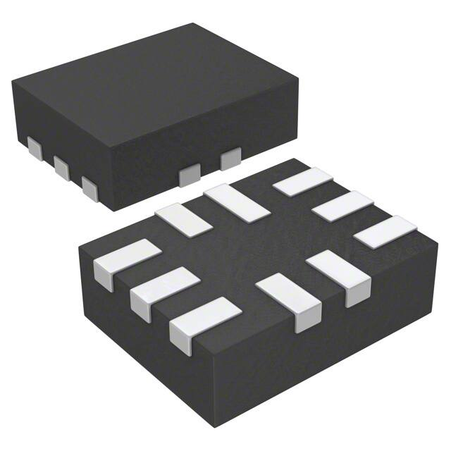
Packaged in ultra small miniQFN-10 (1.4 mm x 1.8 mm x
0.55 mm), it is ideal for portable high speed mix signal
switching application.
As a committed partner to the community and the
environment, Vishay Siliconix manufactures this product with
lead (Pb)-free device termination. The miniQFN-10 package
has a nickel-palladium-gold device termination and is
represented by the lead (Pb)-free “-E4” suffix to the ordering
part number. The nickel-palladium-gold device terminations
meet all JEDEC standards for reflow and MSL rating.
As a further sign of Vishay Siliconix's commitment, the
DG2722 is fully RoHS complaint.
• Halogen-free according to IEC 61249-2-21
Definition
• Wide operation voltage range
• Low on-resistance, 7 (typical at 3 V)
• Low capacitance, CON = 5.8 pF (typical)
• 3 dB high bandwidth: 900 MHz (typical)
• Low bit to bit skew: 40 pS (typical)
• Low power consumption
• Low logic threshold: V
• Power down protection: D+/D- pins can tolerate up to
5 V when V+ = 0 V
• Logic (S and OE) above V+ tolerance
• 8 kV ESD protection (HBM)
• Latch-up current 300 mA per JESD78
• Lead (Pb)-free low profile miniQFN-10 (1.4 mm x 1.8 mm
x 0.55 mm)
• Compliant to RoHS Directive 2002/95/EC
APPLICATIONS
• Cellular phones
•
•
•
•
•
•
Portable media players
PDA
Digital camera
GPS
Notebook computer
TV, monitor, and set top box
FUNCTIONAL BLOCK DIAGRAM AND PIN CONFIGURATION
8
V+
9
S
10
HSD1-
7
6
Control
OE
HSD1+
miniQFN-10L
5
HSD2+
4
HSD2-
3
GND
Rx
1
Top View
Document Number: 68379
S11-2216-Rev. F, 14-Nov-11
D-
D+
Pin 1: LONG LEAD
2
Pin 1
Device marking: Rx for DG2722
x = Date/Lot Traceability Code
www.vishay.com
1
This document is subject to change without notice.
THE PRODUCTS DESCRIBED HEREIN AND THIS DOCUMENT ARE SUBJECT TO SPECIFIC DISCLAIMERS, SET FORTH AT www.vishay.com/doc?91000
�DG2722
Vishay Siliconix
ORDERING INFORMATION
Temp. Range
Package
Part Number
- 40 °C to 85 °C
miniQFN-10
DG2722DN-T1-E4
TRUTH TABLE
PIN DESCRIPTIONS
OE (Pin 8)
S (Pin 10)
Function
Pin Name
Description
0
0
D+ = HSD1+ and D- = HSD1-
OE
Bus Switch Enable
0
1
D+ = HSD2+ and D- = HSD2-
S
Select Input
1
X
Disconnect
HSD1±, HSD2±, D±
Data Port
ABSOLUTE MAXIMUM RATINGS (TA = 25 °C, unless otherwise noted)
Parameter
Limit
Unit
V+
- 0.3 to 5
Reference to GND
V
- 0.3 to (V+ + 0.3)
S, OE, D±, HSD1±, HSD2±a
Current (Any Terminal except S, OE, D±, HSD1±, HSD2±)
30
mA
Continuous Current (S, OE, D±, HSD1±, HSD2±)
± 250
Peak Current (Pulsed at 1 ms, 10 % Duty Cycle)
± 500
Storage Temperature (D Suffix)
- 65 to 150
°C
Power Dissipation (Packages)b
miniQFN-10c
208
mW
ESD (Human Body Model) I/O to GND
8
kV
Latch-up (Current Injection)
300
mA
Notes:
a. Signals on S, OE, D±, HSD1±, HSD2± exceeding V+ will be clamped by internal diodes. Limit forward diode current to maximum current
ratings.
b. All leads welded or soldered to PC board.
c. Derate 2.6 mW/°C above 70 °C.
SPECIFICATIONS (V+ = 3 V)
Parameter
Symbol
Test Conditions
Otherwise Unless Specified
VANALOG
RDS(on)
Limits
- 40 °C to 85 °C
Temp.a Min.b
Typ.c Max.b
Unit
Analog Switch
Analog Signal Ranged
Full
0
Room
V+
7
RDS(on)
V+ = 3 V, ID± = 8 mA, VHSD1/2± = 0.4 V
RON
V+ = 3 V, ID± = 8 mA, VHSD1/2± = 0.4 V
Room
0.8
On-Resistance Resistance
Flatnessd
RON Flatness
V+ = 3 V, ID± = 8 mA, VHSD1/2± = 0 V, 1 V
Room
2
Switch Off Leakage Current
I(off)
V+ = 4.3 V, VHSD1/2± = 0.3 V, 3 V,
VD± = 3 V, 0.3 V
Full
- 100
100
Channel On Leakage Current
I(on)
V+ = 4.3 V, VHSD1/2± = 0.3 V, 4 V,
VD± = 4 V, 0.3 V
Full
- 200
200
V+ = 3 V to 3.6 V
Full
1.3
V+ = 4.3 V
Full
1.5
V+ = 3 V to 4.3 V
Full
VIN = 0 or V+
Full
On-Resistance
On-Resistance Match
d
Full
V
8
9
nA
Digital Control
Input Voltage High
VINH
Input Voltage Low
VINL
Input Capacitance
Input Current
www.vishay.com
2
CIN
IINL or IINH
V
0.5
Full
6.5
-1
pF
1
µA
Document Number: 68379
S11-2216-Rev. F, 14-Nov-11
This document is subject to change without notice.
THE PRODUCTS DESCRIBED HEREIN AND THIS DOCUMENT ARE SUBJECT TO SPECIFIC DISCLAIMERS, SET FORTH AT www.vishay.com/doc?91000
�DG2722
Vishay Siliconix
SPECIFICATIONS (V+ = 3 V)
Parameter
Symbol
Test Conditions
Otherwise Unless Specified
Limits
- 40 °C to 85 °C
Temp.a
Min.b
Typ.c
Max.b
Unit
30
ns
Dynamic Characteristics
Break-Before-Make Timee, d
tBBM
S, OE Turn-On Timee, d
tON
S, OE Turn-Off Timee, d
tOFF
Room
5
Full
V+ = 3 V, VD1/2 ± = 1.5 V, RL = 50 ,
CL = 35 pF
Room
Full
Room
25
Full
Charge Injectiond
QINJ
CL = 1 nF, RGEN = 0 , VGEN = 0 V
0.5
Off-Isolationd
OIRR
- 30
Crosstalkd
XTALK
V+ = 3 V to 3.6 V, RL = 50 , CL = 5 pF,
f = 240 MHz
Bandwidthd
BW
V+ = 3 V to 3.6 V, RL = 50 , - 3 dB
900
D+/D- On Capacitance
CON
V+ = 3.3 V, OE = 0 V, f = 240 MHz
5.8
D1n, D2n Off Capacitance
COFF
V+ = OE = 3.3 V, f = 240 MHz
Channel-to-Channel Skewd
tSK(O)
Skew Off Opposite Transitions of
the Same Outputd
tSK(p)
Total
Jitterd
pC
dB
- 45
Room
MHz
pF
2.2
50
V+ = 3 V to 3.6 V, RL = 50 , CL = 5 pF
20
tJ
ps
200
Power Supply
Power Supply Range
V+
Power Supply Current
I+
2.6
VIN = 0 V, or V+
Full
4.3
V
2
µA
Notes:
a. Room = 25 °C, Full = as determined by the operating suffix.
b. The algebraic convention whereby the most negative value is a minimum and the most positive a maximum, is used in this datasheet.
c. Typical values are for design aid only, not guaranteed nor subject to production testing.
d. Guarantee by design, not subjected to production test.
e. VIN = input voltage to perform proper function.
f. Crosstalk measured between channels.
Stresses beyond those listed under “Absolute Maximum Ratings” may cause permanent damage to the device. These are stress ratings only, and functional operation
of the device at these or any other conditions beyond those indicated in the operational sections of the specifications is not implied. Exposure to absolute maximum
rating conditions for extended periods may affect device reliability.
Document Number: 68379
S11-2216-Rev. F, 14-Nov-11
www.vishay.com
3
This document is subject to change without notice.
THE PRODUCTS DESCRIBED HEREIN AND THIS DOCUMENT ARE SUBJECT TO SPECIFIC DISCLAIMERS, SET FORTH AT www.vishay.com/doc?91000
�DG2722
Vishay Siliconix
TYPICAL CHARACTERISTICS (TA = 25 °C, unless otherwise noted)
30
28
26
V+ = 2.6 V
24
V+ = 3.0 V
V+ = 2.6 V
ION = 8 mA
25
22
RON - On-Resistance (Ω)
RON - On-Resistance (Ω)
T = 25 °C
IS = 8 mA
D1±
V+ = 3.3 V
20
V+ = 3.6 V
18
V+ = 4.3 V
16
14
12
10
8
+ 85 °C
20
+ 25 °C
15
10
- 40 °C
5
6
4
0
0.5
1
1.5
2
2.5
3
3.5
4
4.5
0
5
0
0.5
1
VD - Analog Voltage (V)
RON vs. VD and Single Supply Voltage
2.5
3
25
V+ = 3.0 V
ION = 8 mA
V+ = 3.3 V
ION = 8 mA
+ 85 °C
20
RON - On-Resistance (Ω)
20
RON - On-Resistance (Ω)
2
RON vs. Analog Voltage and Temperature
25
+ 25 °C
15
10
- 40 °C
5
+ 85 °C
15
+ 25 °C
10
- 40 °C
5
0
0.0
0
0
0.5
1
1.5
2
VD - Analog Voltage (V)
2.5
3
0.5
1.0
1.5
2.0
2.5
3.0
3.5
4.0
VD - Analog Voltage (V)
RON vs. Analog Voltage and Temperature
RON vs. Analog Voltage and Temperature
25
25
V+ = 4.3 V
ION = 8 mA
V+ = 3.6 V
ION = 8 mA
20
+ 85 °C
15
+ 25 °C
10
- 40 °C
RON - On-Resistance (Ω)
20
RON - On-Resistance (Ω)
1.5
VD - Analog Voltage (V)
+ 85 °C
15
+ 25 °C
10
- 40 °C
5
5
0
0.0
0.5
1.0
1.5
2.0
2.5
3.0
3.5
VD - Analog Voltage (V)
RON vs. Analog Voltage and Temperature
www.vishay.com
4
4.0
0
0.0
0.5
1.0
1.5
2.0
2.5
3.0
3.5
4.0
4.5
VD - Analog Voltage (V)
RON vs. Analog Voltage and Temperature
Document Number: 68379
S11-2216-Rev. F, 14-Nov-11
This document is subject to change without notice.
THE PRODUCTS DESCRIBED HEREIN AND THIS DOCUMENT ARE SUBJECT TO SPECIFIC DISCLAIMERS, SET FORTH AT www.vishay.com/doc?91000
�DG2722
Vishay Siliconix
TYPICAL CHARACTERISTICS (TA = 25 °C, unless otherwise noted)
10 mA
10 000
V+ = 4.3 V
1 mA
V+ = 3.6 V
1000
Leakage Current (pA)
I+ - Supply Current (A)
V+ = 4.3 V
100 µA
10 µA
V+ = 3.0 V
1 µA
V+ = 3.3 V
V+ = 2.6 V
100 nA
100
ID±(ON)
10
ID±(OFF)
10 nA
ID±(OFF)
1
1 nA
100 pA
10
100
1K
10 K
100 K
1M
0.1
- 60 - 40 - 20
10 M
0
Input Switching Frequency (Hz)
Supply Current vs. Input Switching Frequency
20 40 60 80
Temperature (°C)
100 120 140
Leakage Current vs. Temperature
1.20
0
1.15
-1
1.05
-2
1.00
VIH
0.95
-3
0.90
Gain (dB)
VT - Switching Threshold (V)
1.10
VIL
0.85
0.80
-4
-5
0.75
0.70
-6
0.65
0.60
-7
0.55
0.50
2.5
2.7
2.9
3.1
3.3
3.5
3.7
3.9
4.1
4.3
-8
4.5
1
10
100
1000
Frequency (MHz)
V+ - Supply Voltage (V)
Gain vs. Frequency, V+ = 3.3 V
0
0
- 10
- 10
- 20
- 20
- 30
- 30
Crosstalk (dB)
Off Isolation (dB)
Switching Threshold vs. Supply Voltage
- 40
- 50
- 60
- 40
- 50
- 60
- 70
- 70
- 80
- 80
- 90
- 90
- 100
1
10
100
Frequency (MHz)
Off-Isolation, V+ = 3.3 V
Document Number: 68379
S11-2216-Rev. F, 14-Nov-11
10 000
1000
- 100
1
10
100
1000
Frequency (MHz)
Crosstalk, V+ = 3.3 V
www.vishay.com
5
This document is subject to change without notice.
THE PRODUCTS DESCRIBED HEREIN AND THIS DOCUMENT ARE SUBJECT TO SPECIFIC DISCLAIMERS, SET FORTH AT www.vishay.com/doc?91000
�DG2722
Vishay Siliconix
TEST CIRCUITS
V+
VINH
Logic
Input
HSD1±
or HSD2±
Switch
Input
V+
VINL
Switch Output
D±
tr 5 ns
tf 5 ns
50 %
VOUT
0.9 x V OUT
Logic
Input
Switch
Output
S
RL
50
OE
GND
CL
35 pF
0V
tON
tOFF
0V
Logic "1" = Switch on
Logic input waveforms inverted for switches that have
the opposite logic sense.
CL (includes fixture and stray capacitance)
VOUT D±
(R L
RL
R
ON
)
Figure 1. Switching Time
V+
Logic
Input
V+
VHSD1±
VHSD2±
D±
HSD1±
VINH
tr < 5 ns
tf < 5 ns
VINL
VO
HSD2±
RL
50
S
CL
35 pF
HSD1± = HSD2±
90 %
VO
GND
OE
Switch
0V
Output
tD
tD
CL (includes fixture and stray capacitance)
Figure 2. Break-Before-Make Interval
V+
Rgen
VOUT
V+
HSD1±
or HSD2±
D±
VOUT
VOUT
+
IN
OE
Vgen
CL = 1 nF
VIN = 0 - V+
GND
On
On
Off
S
Q=
OUT
x CL
IN depends on switch configuration: input polarity
determined by sense of switch.
Figure 3. Charge Injection
www.vishay.com
6
Document Number: 68379
S11-2216-Rev. F, 14-Nov-11
This document is subject to change without notice.
THE PRODUCTS DESCRIBED HEREIN AND THIS DOCUMENT ARE SUBJECT TO SPECIFIC DISCLAIMERS, SET FORTH AT www.vishay.com/doc?91000
�DG2722
Vishay Siliconix
TEST CIRCUITS
V+
V+
10 nF
10 nF
V+
V+
HSD1± or HSD2±
OE
D±
0 V, 2.4 V
Meter
D±
OE
0 V, 2.4 V
RL
GND
HSD1±
or HSD2±
S
S
HP4192A
Impedance
Analyzer
or Equivalent
GND
f = 1 MHz
Analyzer
VD±
Off Isolation = 20 log V
HSD2± or HSD1±
Figure 4. Off-Isolation
Figure 5. Channel Off/On Capacitance
Vishay Siliconix maintains worldwide manufacturing capability. Products may be manufactured at one of several qualified locations. Reliability data for Silicon
Technology and Package Reliability represent a composite of all qualified locations. For related documents such as package/tape drawings, part marking, and
reliability data, see www.vishay.com/ppg?68379.
Document Number: 68379
S11-2216-Rev. F, 14-Nov-11
www.vishay.com
7
This document is subject to change without notice.
THE PRODUCTS DESCRIBED HEREIN AND THIS DOCUMENT ARE SUBJECT TO SPECIFIC DISCLAIMERS, SET FORTH AT www.vishay.com/doc?91000
�Package Information
www.vishay.com
Vishay Siliconix
MINI QFN-10L CASE OUTLINE
DIM
MILLIMETERS
INCHES
MIN.
NAM.
MAX.
MIN.
NAM.
MAX.
A
0.45
0.55
0.60
0.0177
0.0217
0.0236
A1
0.00
-
0.05
0.000
-
0.002
b
0.15
0.20
0.25
0.006
0.008
0.010
0.150 or 0.127 REF (1)
c
0.006 or 0.005 REF (1)
D
1.70
1.80
1.90
0.067
0.071
0.075
E
1.30
1.40
1.50
0.051
0.055
0.059
e
0.40 BSC
0.016 BSC
L
0.35
0.40
0.45
0.014
0.016
0.018
L1
0.45
0.50
0.55
0.0177
0.0197
0.0217
Note
(1) The dimension depends on the leadframe that assembly house used.
ECN T16-0163-Rev. B, 16-May-16
DWG: 5957
Revision: 16-May-16
1
Document Number: 74496
THIS DOCUMENT IS SUBJECT TO CHANGE WITHOUT NOTICE. THE PRODUCTS DESCRIBED HEREIN AND THIS DOCUMENT
ARE SUBJECT TO SPECIFIC DISCLAIMERS, SET FORTH AT www.vishay.com/doc?91000
�PAD Pattern
Vishay Siliconix
RECOMMENDED MINIMUM PADS FOR MINI QFN 10L
1.700
(0.0669)
9x
0.563
(0.0221)
0.663
(0.0261)
0.200
(0.0079)
1
2.100
(0.0827)
0.400
(0.0157)
Pitch
10 x
0.225
(0.0089)
Mounting Footprint
Dimensions in mm (inch)
Document Number: 66554
Revision: 05-Mar-10
www.vishay.com
1
�Legal Disclaimer Notice
www.vishay.com
Vishay
Disclaimer
ALL PRODUCT, PRODUCT SPECIFICATIONS AND DATA ARE SUBJECT TO CHANGE WITHOUT NOTICE TO IMPROVE
RELIABILITY, FUNCTION OR DESIGN OR OTHERWISE.
Vishay Intertechnology, Inc., its affiliates, agents, and employees, and all persons acting on its or their behalf (collectively,
“Vishay”), disclaim any and all liability for any errors, inaccuracies or incompleteness contained in any datasheet or in any other
disclosure relating to any product.
Vishay makes no warranty, representation or guarantee regarding the suitability of the products for any particular purpose or
the continuing production of any product. To the maximum extent permitted by applicable law, Vishay disclaims (i) any and all
liability arising out of the application or use of any product, (ii) any and all liability, including without limitation special,
consequential or incidental damages, and (iii) any and all implied warranties, including warranties of fitness for particular
purpose, non-infringement and merchantability.
Statements regarding the suitability of products for certain types of applications are based on Vishay's knowledge of typical
requirements that are often placed on Vishay products in generic applications. Such statements are not binding statements
about the suitability of products for a particular application. It is the customer's responsibility to validate that a particular product
with the properties described in the product specification is suitable for use in a particular application. Parameters provided in
datasheets and / or specifications may vary in different applications and performance may vary over time. All operating
parameters, including typical parameters, must be validated for each customer application by the customer's technical experts.
Product specifications do not expand or otherwise modify Vishay's terms and conditions of purchase, including but not limited
to the warranty expressed therein.
Hyperlinks included in this datasheet may direct users to third-party websites. These links are provided as a convenience and
for informational purposes only. Inclusion of these hyperlinks does not constitute an endorsement or an approval by Vishay of
any of the products, services or opinions of the corporation, organization or individual associated with the third-party website.
Vishay disclaims any and all liability and bears no responsibility for the accuracy, legality or content of the third-party website
or for that of subsequent links.
Except as expressly indicated in writing, Vishay products are not designed for use in medical, life-saving, or life-sustaining
applications or for any other application in which the failure of the Vishay product could result in personal injury or death.
Customers using or selling Vishay products not expressly indicated for use in such applications do so at their own risk. Please
contact authorized Vishay personnel to obtain written terms and conditions regarding products designed for such applications.
No license, express or implied, by estoppel or otherwise, to any intellectual property rights is granted by this document or by
any conduct of Vishay. Product names and markings noted herein may be trademarks of their respective owners.
© 2022 VISHAY INTERTECHNOLOGY, INC. ALL RIGHTS RESERVED
Revision: 01-Jan-2022
1
Document Number: 91000
�


 工商网监
湘ICP备2023018690号
工商网监
湘ICP备2023018690号
