DG2741, DG2742, DG2743
Vishay Siliconix
Low-Voltage, 0.8 RON, Dual SPST Analog Switch
DESCRIPTION
FEATURES
The DG2741, DG2742, DG2743 are low voltage, single
supply, dual SPST analog switches. Designed for high
performance switching of analog signals, the DG2741,
DG2742, DG2743 provide low on-resistance (0.8 at
+ 2.7 V), fast speed (tON, tOFF at 35 ns and 33 ns) and the
ability to handle signals over the entire analog voltage range.
•
•
•
•
•
•
•
•
When operated on a + 3 V supply, control pins are
compatible with 1.8 V digital logic. Additionally, onresistance flatness and matching (0.18 and 0.08 ,
respectively) offer high accuracy between channels.
The DG2741 contains two normally open (NO) switches, the
DG2742 contains two normally closed (NC) switches, and
the DG2743 contains one normally open and one normally
closed switch. Break-before-make is guaranteed.
Built on Vishay Siliconix’s low voltage submicron CMOS
process, the DG2741, DG2742, DG2743 were designed to
offer solutions that extend beyond audio/video functions, to
providing the performance required for today’s demanding
mixed-signal switching in portable applications.
Low voltage operation (1.6 V to 3.6 V)
Low on-resistance - RDS(on): 0.8 at 2.7 V
High current handling capacity: 150 mA continuous
Off-isolation: - 56 dB at 1 MHz
Fast switching: 25 ns tON
Low charge injection - QINJ: 5.8 pC
Low power consumption: < 1 µW
ESD protection > 2 000 V
BENEFITS
•
•
•
•
•
High accuracy
High bandwidth
TTL and low voltage logic compatibility
Low power consumption
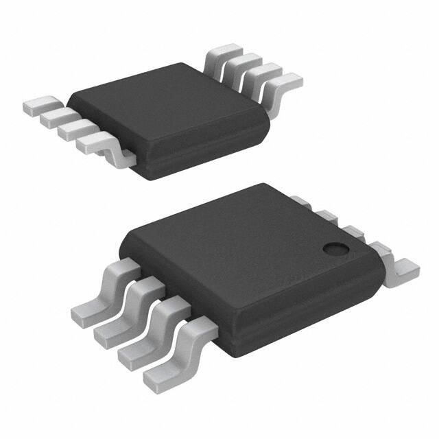
Reduced PCB space (SOT23-8 and MSOP-8)
APPLICATIONS
•
•
•
•
•
Mixed signal routing
Portable and battery operated systems
Low voltage data acquisition
Modems
PCMCIA cards
FUNCTIONAL BLOCK DIAGRAM AND PIN CONFIGURATION (DG2741)
DG2741, MSOP-8
DG2741, SOT23-8
NO1
1
8
V+
IN1
1
8
NO1
COM1
2
7
IN1
V+
2
7
COM1
IN2
3
6
COM2
NO2
3
6
IN2
GND
4
5
NO2
COM2
4
5
GND
Top View
Top View
Device Marking: 2741
Device Marking: F3
TRUTH TABLE (DG2741)
Logic
Switch
0
Off
1
On
Document Number: 72708
S11-0303-Rev. B, 28-Feb-11
www.vishay.com
1
�DG2741, DG2742, DG2743
Vishay Siliconix
FUNCTIONAL BLOCK DIAGRAM AND PIN CONFIGURATION (DG2742, DG2743)
DG2742, MSOP-8
NC1
1
DG2742, SOT23-8
8
V+
IN1
1
8
NC1
V+
2
7
COM1
NC2
3
6
IN2
COM2
4
5
GND
COM1
2
7
IN1
IN2
3
6
COM2
5
NC2
GND
4
Top View
Top View
Device Marking: 2742
Device Marking: F4
TRUTH TABLE (DG2742)
Logic
Switch
0
On
1
Off
DG2743, MSOP-8
DG2743, SOT23-8
NO1
1
8
V+
IN1
1
8
NO1
COM1
2
7
IN1
V+
2
7
COM1
IN2
3
6
COM2
NC2
3
6
IN2
GND
4
5
NC2
COM2
4
5
GND
Top View
Top View
Device Marking: F5
Device Marking: 2743
TRUTH TABLE (DG2743)
Logic
Switch-1
Switch-2
0
Off
On
1
On
Off
ORDERING INFORMATION
Temp. Range
Package
Part Number
DG2741DQ-T1
MSOP-8
DG2742DQ-T1
DG2743DQ-T1
- 40 °C to 85 °C
DG2741DS-T1
SOT23-8
DG2742DS-T1
DG2743DS-T1
www.vishay.com
2
Document Number: 72708
S11-0303-Rev. B, 28-Feb-11
�DG2741, DG2742, DG2743
Vishay Siliconix
ABSOLUTE MAXIMUM RATINGS (TA = 25 °C, unless otherwise noted)
Parameter
Limit
Referenced V+ to GND
Unit
- 0.3 to + 4 V
IN, COM, NC, NOa
Continuous Current (NO, NC and COM Pins)
V
- 0.3 V to (V+ + 0.3 V)
± 200
Peak Current (Pulsed at 1 ms, 10 % duty cycle)
mA
± 300
ESD per Method 3015.7
>2
Storage Temperature (D Suffix)
Power Dissipation (Packages)c
kV
- 65 to 150
°C
250
mW
6-Pin SC-70c
Notes:
a. Signals on NC, NO, or COM or IN exceeding V+ will be clamped by internal diodes. Limit forward diode current to maximum current ratings.
b. All leads welded or soldered to PC board.
c. Derate 3.1 mW/°C above 70 °C.
SPECIFICATIONS (V+ = 1.8 V)
Parameter
Symbol
Test Conditions
Otherwise Unless Specified
V+ = 1.8 V, ± 10 %, VIN = 0.4 or 1.0 Ve
Limits
- 40 °C to 85 °C
Temp.a
Min.b
Full
0
Typ.c
Max.b
Unit
V+
V
Analog Switch
VNO, VNC
VCOM
Analog Signal Ranged
On-Resistance
RON
RON Flatnessd
RON
Flatness
RON
RON Matchd
Switch Off Leakage Current
f
INO(off)
INC(off)
ICOM(off)
Channel-On Leakage Currentf
ICOM(on)
V+ = 1.8 V, VCOM = 0.9 V
INO, INC = 10 mA
V+ = 1.8 V, VCOM = 0 to V+, INO, INC = 10 mA
V+ = 1.8 V
VNO, VNC = 0.2 V/2.0 V, VCOM = 1.5 V/0.3 V
V+ = 1.8 V, VNO, VNC = VCOM = 0.3 V/1.5 V
Room
Fulld
0.9
Room
0.25
Room
0.05
2.5
4.0
Room
Fulld
-1
- 10
1
10
Room
Fulld
-1
- 10
1
10
Room
Fulld
-1
- 10
1
10
1.0
nA
Digital Control
Input High Voltage
VINH
Full
Input Low Voltage
VINL
Full
Input Capacitanced
f
Cin
IINL or IINH
Input Current
0.4
Full
VIN = 0 or V+
Full
5.5
-1
V
pF
1
µA
Dynamic Characteristics
Turn-On Timed
tON
Turn-Off Timed
tOFF
Break-Before-Make Timed
Charge Injection
Off-Isolation
d
d
Crosstalkd
td
QINJ
OIRR
XTALK
NO, NC Off Capacitanced
CNO(off)
CNC(off)
Channel-On Capacitanced
CON
Document Number: 72708
S11-0303-Rev. B, 28-Feb-11
VNO or VNC = 1.5 V, RL = 50 , CL = 35 pF
figures 1 and 2
Room
Fulld
33
45
50
Room
Fulld
27
40
45
Room
CL = 1 nF, VGEN = 0 V, RGEN = 0 , figure 3
RL = 1 k, CL = 5 pF, f = 1 MHz
VIN = 0 or V+, f = 1 MHz
ns
3
Room
20
Room
55
Room
91
Room
88
Room
105
pC
dB
pF
www.vishay.com
3
�DG2741, DG2742, DG2743
Vishay Siliconix
SPECIFICATIONS (V+ = 3.0 V)
Parameter
Symbol
Test Conditions
Otherwise Unless Specified
V+ = 3 V, ± 10 %, VIN = 0.5 or 1.4 Ve
Limits
- 40 °C to 85 °C
Temp.a
Min.b
Full
0
Typ.c
Max.b
Unit
V+
V
Analog Switch
Analog Signal Ranged
VNO, VNC
VCOM
RON
On-Resistance
RON
Flatness
RON Flatness
RON
RON MatchFlat
Switch Off Leakage Current
INO(off)
INC(off)
ICOM(off)
Channel-On Leakage Current
ICOM(on)
V+ = 2.7 V, VCOM = 0.2 V/1.5 V, INO
INC = 100 mA
V+ = 2.7 V, VCOM = 1.5, 2 V, INO, INC = 100 mA
V+ = 3.3 V
VNO, VNC = 0.3 V/3 V, VCOM = 3 V/0.3 V
V+ = 3.3 V, VNO, VNC = VCOM = 0.3 V/3 V
Room
Full
0.4
0.8
0.9
Room
0.8
0.18
Room
0.05
0.08
Room
Full
-1
- 10
1
10
Room
Full
-1
- 10
1
10
Room
Full
-1
- 10
1
10
1.4
nA
Digital Control
Input High Voltage
VINH
Full
Input Low Voltage
VINL
Full
Input Capacitanced
f
Cin
IINL or IINH
Input Current
0.5
Full
VIN = 0 or V+
Full
5.5
-1
V
pF
1
µA
Dynamic Characteristics
Turn-On Time
tON
Turn-Off Time
tOFF
Break-Before-Make Time
Charge Injection
d
d
td
QINJ
Off-Isolation
OIRR
Crosstalkd
XTALK
NO, NC Off Capacitanced
Channel-On
Capacitanced
VNO or VNC = 1.5 V, RL = 50 , CL = 35 pF
V+ = 2.7 V, figures 1 and 2
CNO(off)
CNC(off)
Room
Full
20
30
35
Room
Full
18
28
33
Room
CL = 1 nF, VGEN = 0 V, RGEN = 0 , figure 3
RL = 1 k, CL = 5 pF, f = 1 MHz
V+ = 3.6 V, VIN = 0 or V+, f = 1 MHz
CON
ns
1
Room
5.8
Room
- 56
Room
- 89
Room
81
Room
103
pC
dB
pF
Power Supply
Power Supply Range
V+
Power Supply Current
I+
1.5
V+ = 3.6 V, VIN = 0 or V+
0.01
3.6
V
1.0
µA
Notes:
a. Room = 25 °C, Full = as determined by the operating suffix.
b. The algebraic convention whereby the most negative value is a minimum and the most positive a maximum, is used in this data sheet.
c. Typical values are for design aid only, not guaranteed nor subject to production testing.
d. Guarantee by design, nor subjected to production test.
e. VIN = input voltage to perform proper function.
f. Guaranteed by 3 V leakage testing, not production tested.
Stresses beyond those listed under “Absolute Maximum Ratings” may cause permanent damage to the device. These are stress ratings only, and functional operation
of the device at these or any other conditions beyond those indicated in the operational sections of the specifications is not implied. Exposure to absolute maximum
rating conditions for extended periods may affect device reliability.
www.vishay.com
4
Document Number: 72708
S11-0303-Rev. B, 28-Feb-11
�DG2741, DG2742, DG2743
Vishay Siliconix
TYPICAL CHARACTERISTICS (25 °C, unless otherwise noted)
0.7
0.7
85 °C
25 °C
V+ = 1.8 V
V+ = 1.8 V, NC
0.6
0.6
- 40 °C
0.5
0.5
)
0.4
0.3
RDS(on)(
RDS (on)
()
V+ = 1.8 V, NO
V+ = 2.7 V, NO
V+ = 2.7 V, NC
V+ = 2.7 V
0.3
85 °C
0.2
0.2
0.1
0.1
0.0
0.00 0.25 0.50 0.75 1.00 1.25 1.50 1.75 2.00 2.25 2.50 2.75
0.0
0.00 0.25 0.50 0.75 1.00 1.25 1.50 1.75 2.00 2.25 2.50 2.75
25 °C
- 40 °C
VD (V)
VD (V)
RDS(on) vs. VCOM vs. 1 VCC
RDS(on) vs. VD, VCC and Temperature
10000
10 000
V+ = 3.6 V
1000
1000
Power Supply Current (µA)
ICC Supply Current (pA)
0.4
VIN = 0 V
100
VIN = 3.6 V
10
100
10
1
0.1
1
- 40
0.01
- 20
0
20
40
60
80
100
0.01 K 0.1 K 1 K 10 K 100 K
1M
10 M 100 M
Temperature (°C)
Input Switching Frequency (Hz)
Supply Current vs. Temperature
Switching Frequency vs. Supply Current
1G
2000
10 000
V+ = 3.3 V
1500
IS(off)
1000
1000
Leakage Current (pA)
Leakage Current (pA)
V+ = 3.5 V
ID(off)
100
IS(off)
500
0
- 500
ID(on)
- 1000
10
- 1500
ID(off)
ID(on)
1
- 50
- 25
0
25
50
75
Temperature (°C)
Leakage Current vs. Temperature
Document Number: 72708
S11-0303-Rev. B, 28-Feb-11
100
- 2000
0.0
0.5
1.0
1.5
2.0
2.5
3.0
3.5
VD (V)
Leakage Current vs. Analog Voltage
www.vishay.com
5
�DG2741, DG2742, DG2743
Vishay Siliconix
TYPICAL CHARACTERISTICS (25 °C, unless otherwise noted)
50
10
45
LOSS
Loss, OIRR, XTALK (dB)
t ON, t OFF - Switching Time (ns)
- 10
40
tON, V+ = 1.8 V
35
tOFF, V+ = 1.8 V
30
25
tON, V+ = 2.7 V
20
tOFF, V+ = 2.7 V
15
- 30
- 50
v+ = 3.6 v
v+ = 1.8 v
- 70
OIRR
XTALK
- 90
10
- 110
5
0
- 40
- 20
0
20
40
60
80
- 130
10 K
100
1M
100 K
Temperature (°C)
10 M
100 M
1G
Frequency (Hz)
Switching Time vs. VCC and Temperature
Insertion Loss, Off -Isolation
Crosstalk vs. Frequency
2.0
40
1.6
20
Q - Charge Injection (pC)
V T - Switching Threshold (V)
1.8
1.4
1.2
1.0
0.8
0.6
0.4
V+ = 3.6 V
0
V+ = 1.8 V
- 20
- 40
0.2
0.0
0
1
2
3
4
5
V+ - Supply Voltage (V)
Switching Threshold vs. Supply Voltage
www.vishay.com
6
6
- 60
0.0
0.5
1.0
1.5
2.0
2.5
3.0
3.5
4.0
VCOM - Analog Voltage (v)
Charge Injection vs. Analog Voltage
Document Number: 72708
S11-0303-Rev. B, 28-Feb-11
�DG2741, DG2742, DG2743
Vishay Siliconix
TEST CIRCUITS
V+
VINH
Logic
Input
50 %
VINL
V+
NO or NC
Switch
Input
tr < 5 ns
tf < 5 ns
Switch Output
COM
VOUT
0.9 x VOUT
Switch
Output
IN
Logic
Input
RL
50
GND
CL
35 pF
0V
tOFF
tON
Logic “1” = Switch On
Logic input waveforms inverted for switches that have
the opposite logic sense.
CL (includes fixture and stray capacitance)
V OUT = V COM
RL
R L + R ON
Figure 1. Switching Time
V+
VOUT
V+
Rgen
COM
NC or NO
VOUT
VOUT
+
IN
Vgen
IN
CL = 1 nF
On
Off
On
GND
Q = VOUT x CL
VIN = 0 - V+
IN depends on switch configuration: input polarity
determined by sense of switch.
Figure 2.Charge Injection
V+
10 nF
V+
10 nF
V+
NC or NO
IN
V+
0 V, 2.4 V
COM
COM
Meter
IN
0 V, 2.4 V
RL
GND
NC or NO
Analyzer
GND
HP4192A
Impedance
Analyzer
or Equivalent
f = 1 MHz
V COM
Off Isolation = 20 log V
NO/ NC
Figure 3. Off-Isolation
Figure 4. Channel Off/On Capacitance
Vishay Siliconix maintains worldwide manufacturing capability. Products may be manufactured at one of several qualified locations. Reliability data for Silicon
Technology and Package Reliability represent a composite of all qualified locations. For related documents such as package/tape drawings, part marking, and
reliability data, see www.vishay.com/ppg?72708.
Document Number: 72708
S11-0303-Rev. B, 28-Feb-11
www.vishay.com
7
�Package Information
Vishay Siliconix
MSOP:
8−LEADS
JEDEC Part Number: MO-187, (Variation AA and BA)
(N/2) Tips)
2X
5
A B C 0.20
N N-1
0.60
0.48 Max
Detail “B”
(Scale: 30/1)
Dambar Protrusion
E
1 2
0.50
N/2
0.60
0.08 M C B S
b
A S
7
Top View
b1
e1
With Plating
e
A
See Detail “B”
c1
0.10 C
-H-
A1
D
6
Seating Plane
c
Section “C-C”
Scale: 100/1
(See Note 8)
Base Metal
-A-
3
See Detail “A”
Side View
0.25
BSC
C
Parting Line
0.07 R. Min
2 Places
Seating Plane
ς
A2
0.05 S
C
E1
-B-
L 4
T
-C-
3
0.95
End View
Detail “A”
(Scale: 30/1)
N = 8L
NOTES:
1.
Die thickness allowable is 0.203"0.0127.
2.
Dimensioning and tolerances per ANSI.Y14.5M-1994.
3.
Dimensions “D” and “E1” do not include mold flash or protrusions, and are
measured at Datum plane -H- , mold flash or protrusions shall not exceed
0.15 mm per side.
4.
Dimension is the length of terminal for soldering to a substrate.
5.
Terminal positions are shown for reference only.
6.
Formed leads shall be planar with respect to one another within 0.10 mm at
seating plane.
7.
The lead width dimension does not include Dambar protrusion. Allowable
Dambar protrusion shall be 0.08 mm total in excess of the lead width
dimension at maximum material condition. Dambar cannot be located on the
lower radius or the lead foot. Minimum space between protrusions and an
adjacent lead to be 0.14 mm. See detail “B” and Section “C-C”.
8.
Section “C-C” to be determined at 0.10 mm to 0.25 mm from the lead tip.
9.
Controlling dimension: millimeters.
10. This part is compliant with JEDEC registration MO-187, variation AA and BA.
11. Datums -A- and -B- to be determined Datum plane -H- .
MILLIMETERS
Dim
Min
Nom
Max
A
A1
A2
b
b1
c
c1
D
E
E1
e
e1
L
N
T
-
-
1.10
0.05
0.10
0.15
0.75
0.85
0.95
0.25
-
0.38
8
0.25
0.30
0.33
8
0.13
-
0.23
0.15
0.18
0.13
3.00 BSC
Note
3
4.90 BSC
2.90
3.00
3.10
3
0.70
4
0.65 BSC
1.95 BSC
0.40
0.55
8
0_
4_
5
6_
ECN: T-02080—Rev. C, 15-Jul-02
DWG: 5867
12. Exposed pad area in bottom side is the same as teh leadframe pad size.
Document Number: 71244
12-Jul-02
www.vishay.com
1
�Package Information
Vishay Siliconix
SOT−23 :
8−LEAD
b
e
CL
E1
CL
E
e1
D
CL
A
CL
A2
T
A1
DATUM A
- A-
E1
C
0.10
L
MILLIMETERS
NOTES:
1.
All dimensions are in millimeters.
2.
Foot length measured at intercept point between Datum A and
lead surface.
3.
4.
5.
2
0.20
- A-
Package outline exclusive of mold flash and metal burr.
Package outline inclusive of solder plating.
No molding flash allowed on the top and bottom lead surface.
Dim
Min
A
A1
A2
b
C
D
E
E1
e
e1
L
T
INCHES
Nom
Max
Min
Nom
Max
0.90
1.27
1.45
0.00
0.0762
0.15
0.035
0.05
0.057
0.000
0.003
0.90
1.20
0.006
1.30
0.035
0.047
0.051
0.22
0.09
0.30
0.38
0.009
0.012
0.015
0.152
0.20
0.004
0.006
2.80
0.008
2.9
3.00
0.11
0.114
0.118
2.60
2.8
23.00
0.102
0.11
0.118
1.50
1.65
1.75
0.059
0.065
0.069
0.65 REF
0.026 REF
1.95 REF
0.077 REF
0.35
0.45
0.55
0.014
0.018
0.022
0_
4_
8_
0_
4_
8_
ECN: C-03085—Rev. A, 07-Apr-03
DWG: 5895
Document Number: 72207
09-Apr-03
www.vishay.com
1
�Legal Disclaimer Notice
www.vishay.com
Vishay
Disclaimer
ALL PRODUCT, PRODUCT SPECIFICATIONS AND DATA ARE SUBJECT TO CHANGE WITHOUT NOTICE TO IMPROVE
RELIABILITY, FUNCTION OR DESIGN OR OTHERWISE.
Vishay Intertechnology, Inc., its affiliates, agents, and employees, and all persons acting on its or their behalf (collectively,
“Vishay”), disclaim any and all liability for any errors, inaccuracies or incompleteness contained in any datasheet or in any other
disclosure relating to any product.
Vishay makes no warranty, representation or guarantee regarding the suitability of the products for any particular purpose or
the continuing production of any product. To the maximum extent permitted by applicable law, Vishay disclaims (i) any and all
liability arising out of the application or use of any product, (ii) any and all liability, including without limitation special,
consequential or incidental damages, and (iii) any and all implied warranties, including warranties of fitness for particular
purpose, non-infringement and merchantability.
Statements regarding the suitability of products for certain types of applications are based on Vishay's knowledge of typical
requirements that are often placed on Vishay products in generic applications. Such statements are not binding statements
about the suitability of products for a particular application. It is the customer's responsibility to validate that a particular product
with the properties described in the product specification is suitable for use in a particular application. Parameters provided in
datasheets and / or specifications may vary in different applications and performance may vary over time. All operating
parameters, including typical parameters, must be validated for each customer application by the customer's technical experts.
Product specifications do not expand or otherwise modify Vishay's terms and conditions of purchase, including but not limited
to the warranty expressed therein.
Hyperlinks included in this datasheet may direct users to third-party websites. These links are provided as a convenience and
for informational purposes only. Inclusion of these hyperlinks does not constitute an endorsement or an approval by Vishay of
any of the products, services or opinions of the corporation, organization or individual associated with the third-party website.
Vishay disclaims any and all liability and bears no responsibility for the accuracy, legality or content of the third-party website
or for that of subsequent links.
Except as expressly indicated in writing, Vishay products are not designed for use in medical, life-saving, or life-sustaining
applications or for any other application in which the failure of the Vishay product could result in personal injury or death.
Customers using or selling Vishay products not expressly indicated for use in such applications do so at their own risk. Please
contact authorized Vishay personnel to obtain written terms and conditions regarding products designed for such applications.
No license, express or implied, by estoppel or otherwise, to any intellectual property rights is granted by this document or by
any conduct of Vishay. Product names and markings noted herein may be trademarks of their respective owners.
© 2022 VISHAY INTERTECHNOLOGY, INC. ALL RIGHTS RESERVED
Revision: 01-Jan-2022
1
Document Number: 91000
�


 工商网监
湘ICP备2023018690号
工商网监
湘ICP备2023018690号
