DG441B, DG442B
Vishay Siliconix
Improved Quad SPST CMOS Analog Switches
FEATURES
DESCRIPTION
The DG441B, DG442B are monolithic quad analog switches
designed to provide high speed, low error switching of
analog and audio signals. The DG441B, DG442B are
upgrades to the original DG441, DG442.
Combing low on-resistance (45 , typ.) with high speed
(tON 120 ns, typ.), the DG441B, DG442B are ideally
suited for Data Acquisition, Communication Systems,
Automatic Test Equipment, or Medical Instrumentation.
Charge injection has been minimized on the drain for use in
sample-and-hold circuits.
The DG441B, DG442B are built using Vishay Siliconix’s
high-voltage silicon-gate process. An epitaxial layer prevents
latchup.
When on, each switch conducts equally well in both
directions and blocks input voltages to the supply levels
when off.
•
•
•
•
•
•
•
Low On-Resistance: 45
Low Power Consumption: 1 mW
Fast Switching Action - tON: 120 ns
Low Charge Injection - Q: - 1 pC
TTL/CMOS-Compatible Logic
Single Supply Capability
Material categorization: For definitions of
compliance please see www.vishay.com/doc?99912
BENEFITS
•
•
•
•
•
Less Signal Errors and Distortion
Reduced Power Supply Requirements
Faster Throughput
Reduced Pedestal Errors
Simple Interfacing
APPLICATIONS
•
•
•
•
•
•
Audio Switching
Data Acquisition
Sample-and-Hold Circuits
Communication Systems
Automatic Test Equipment
Medical Instruments
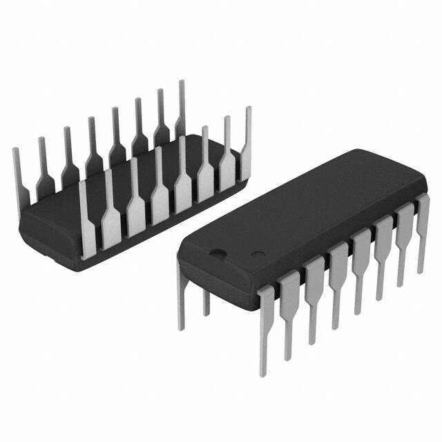
FUNCTIONAL BLOCK DIAGRAM AND PIN CONFIGURATION
DG441B
Dual-In-Line and SOIC
IN1
1
16
IN2
D1
2
15
D2
S1
3
14
S2
V-
4
13
V+
GND
5
12
NC
S4
6
11
S3
D4
7
10
D3
IN4
8
9
IN3
TRUTH TABLE
Logic
DG441B
DG442B
0
ON
OFF
1
OFF
ON
Logic "0" 0.8 V
Logic "1" 2.4 V
Top View
ORDERING INFORMATION
DG441B
QFN16 (4 x 4 mm)
Temp Range
Package
DG441BDJ
D1 IN1 IN2 D2
16
15
14
13
16-pin Plastic DIP
S1
1
12
S2
V-
2
11
V+
GND
3
10
NC
S4
4
9
S3
5
6
7
8
Part Number
DG441BDJ-E3
DG442BDJ
DG442BDJ-E3
DG441BDY-E3
- 40 °C to 85 °C
16-pin Narrow SOIC
DG441BDY-T1-E3
DG442BDY-E3
DG442BDY-T1-E3
16 pin QFN 4 x 4 mm
(Variation 1)
DG441BDN-T1-E4
DG442BDN-T1-E4
D4 IN4 IN3 D3
Top View
Document Number: 72625
S13-1284-Rev. C, 27-May-13
For technical questions, contact: pmostechsupport@vishay.com
www.vishay.com
1
This document is subject to change without notice.
THE PRODUCTS DESCRIBED HEREIN AND THIS DOCUMENT ARE SUBJECT TO SPECIFIC DISCLAIMERS, SET FORTH AT www.vishay.com/doc?91000
�DG441B, DG442B
Vishay Siliconix
ABSOLUTE MAXIMUM RATINGS (TA = 25 °C, unless otherwise noted)
Parameter
Symbol
Limit
V+ to VGND to VDigital
Inputsa
Unit
44
25
(V-) - 2 to (V+) + 2 or
30 mA, whichever occurs first
, VS, VD
Continuous Current (Any Terminal)
30
Current, S or D (Pulsed at 1 ms, 10 % duty cycle )
100
Storage Temperature
- 65 to 125
16-pin Plastic DIP
b
Power Dissipation (Package)
c
16-pin Narrow Body
QFN-16
V
mA
°C
470
SOICd
d
900
mW
850
Notes:
a. Signals on SX, DX, or INX exceeding V+ or V- will be clamped by internal diodes. Limit forward diode current to maximum current ratings.
b. All leads welded or soldered to PC Board.
c. Derate 6 mW/°C above 75 °C.
d. Derate 12 mW/°C above 75 °C.
www.vishay.com
2
For technical questions, contact: pmostechsupport@vishay.com
Document Number: 72625
S13-1284-Rev. C, 27-May-13
This document is subject to change without notice.
THE PRODUCTS DESCRIBED HEREIN AND THIS DOCUMENT ARE SUBJECT TO SPECIFIC DISCLAIMERS, SET FORTH AT www.vishay.com/doc?91000
�DG441B, DG442B
Vishay Siliconix
SPECIFICATIONSa (for dual supplies)
Limits
- 40 °C to 85 °C
Test Conditions
Unless Otherwise Specified
V+ = 15 V, V- = - 15 V
VL = 5 V, VIN = 2.4 V, 0.8 Ve
Temp.b
Min.d
VANALOG
Full
- 15
RDS(on)
RDS(on)
Parameter
Analog Switch
Symbol
Analog Signal Rangee
Drain-Source
On-Resistance
On-Resistance Match Between
Channels
e
Typ.c
Max.d
Unit
15
V
IS = 1 mA, VD = ± 10 V
Room
Full
45
80
95
IS = 1 mA, VD = ± 10 V
Room
Full
2
4
5
± 0.01
0.5
5
0.5
5
0.5
10
IS(off)
VD = ± 14 V, VS = ± 14 V
Switch Off Leakage Current
ID(off)
Channel On Leakage Current
ID(on)
VS = VD = ± 14 V
Room
Full
Room
Full
Room
Full
- 0.5
-5
- 0.5
-5
- 0.5
- 10
± 0.01
± 0.02
nA
Digital Control
Input Voltage Low
VINL
Full
Input Voltage High
VINH
Full
2.4
Input Current VIN Low
IINL
Full
-1
- 0.01
1
Input Current VIN High
IINH
Full
-1
0.01
1
VIN under test = 0.8 V
All Other = 2.4 V
VIN under test = 2.4 V
All Other = 0.8 V
0.8
V
µA
Dynamic Characteristics
Turn-On Time
tON
Turn-Off Time
tOFF
Charge Injectione
Off Isolatione
Crosstalk (Channel-to-Channel)
Q
OIRR
XTALK
SourceOff Capacitancee
CS(off)
Drain Off Capacitancee
CD(off)
Capacitancee
Channel On
Power Supplies
CD(on)
Positive Supply Current
I+
Negative Supply Current
I-
Document Number: 72625
S13-1284-Rev. C, 27-May-13
Room
120
220
Room
65
120
Room
-1
Room
- 90
Room
Room
- 95
Room
4
VS = VD = 0 V, f = 1 MHz
Room
16
V+ = 16.5 V, V- = - 16.5 V
VIN = 0 or 5 V
Room
Full
Room
Full
RL = 1 k, CL = 35 pF
VS = 10 V, See Figure 2
CL = 1 nF, VS = 0 V
Vgen = 0 V, Rgen = 0
RL = 50 , CL = 15 pF
VS = 1 VRMS, f = 100 kHz
f = 1 MHz
For technical questions, contact: pmostechsupport@vishay.com
ns
pC
dB
4
pF
1
5
-1
-5
µA
www.vishay.com
3
This document is subject to change without notice.
THE PRODUCTS DESCRIBED HEREIN AND THIS DOCUMENT ARE SUBJECT TO SPECIFIC DISCLAIMERS, SET FORTH AT www.vishay.com/doc?91000
�DG441B, DG442B
Vishay Siliconix
SPECIFICATIONS (for single supply)
Test Conditions
Unless Otherwise Specified
V+ = 12 V, V- = 0 V
Limits
- 40 °C to 85 °C
VIN = 2.4 V, 0.8 Ve
Temp.b
Min.d
VANALOG
Full
0
RDS(on)
IS = 1 mA, VD = 3 V, 8 V
Turn-On Time
tON
Turn-Off Time
tOFF
Q
Parameter
Analog Switch
Symbol
Analog Signal Rangee
Drain-Source
On-Resistance
Dynamic Characteristics
Charge Injection
Typ.c
Max.d
Unit
12
V
Room
Full
90
160
200
RL = 1 k, CL = 35 pF, VS = 8 V
See Figure 2
Room
120
300
Room
60
200
CL = 1 nF, Vgen = 6 V, Rgen = 0
Room
4
VIN = 0 V or 5 V
Room
Full
Room
Full
ns
pC
Power Supplies
Positive Supply Current
I+
Negative Supply Current
I-
1
5
-1
-5
µA
Notes:
a. Refer to PROCESS OPTION FLOWCHART.
b. Room = 25 °C, Full = as determined by the operating temperature suffix.
c. Typical values are for DESIGN AID ONLY, not guaranteed nor subject to production testing.
d. The algebraic convention whereby the most negative value is a minimum and the most positive a maximum, is used in this data sheet.
e. Guaranteed by design, not subject to production test.
f. VIN = input voltage to perform proper function.
Stresses beyond those listed under “Absolute Maximum Ratings” may cause permanent damage to the device. These are stress ratings only, and functional operation
of the device at these or any other conditions beyond those indicated in the operational sections of the specifications is not implied. Exposure to absolute maximum
rating conditions for extended periods may affect device reliability.
SCHEMATIC DIAGRAM (typical channel)
V+
5 V Reg
INX
V-
Level
Shift/
Drive
V+
GND
V-
Figure 1.
www.vishay.com
4
For technical questions, contact: pmostechsupport@vishay.com
Document Number: 72625
S13-1284-Rev. C, 27-May-13
This document is subject to change without notice.
THE PRODUCTS DESCRIBED HEREIN AND THIS DOCUMENT ARE SUBJECT TO SPECIFIC DISCLAIMERS, SET FORTH AT www.vishay.com/doc?91000
�DG441B, DG442B
Vishay Siliconix
TYPICAL CHARACTERISTICS (TA = 25 °C, unless otherwise noted)
110
100
100
90
80
±5V
80
70
R DS(on) (Ω)
RDS(on) (Ω)
90
V+ = 15 V
V- = - 15 V
70
± 10 V
60
50
± 15 V
40
± 20 V
30
60
125 °C
85 °C
50
40
25 °C
30
- 55 °C
20
20
10
10
- 20 - 16 - 12
-8
-4
0
4
8
12
16
0
- 15
20
- 10
-5
VD – Drain Voltage (V)
VD
RDS(on) vs. VD and Power Supply Voltages
5
10
15
RDS(on) vs. VD and Temperature
250
2.5
225
V+ = 5 V
200
2
175
150
VTH (V)
RDS(on) (Ω)
0
Drain Voltage (V)
7V
125
10 V
100
1.5
1
12 V
15 V
75
50
0.5
25
0
0
2
4
6
8
10
12
VD – Drain Voltage (V)
14
0
16
4
8
10
12
14
16
18
20
V+ Positive Supply (V)
RDS(on) vs. VD and Single Power Supply Voltages
Input Switching Threshold vs. Supply Voltage
80
60
6
1 nA
V+ = 22 V
V- = - 22 V
TA = 25 °C
V+ = 15 V
V- = - 15 V
VS, V D = ± 14 V
IS, ID - Current
I S, I D – Current (pA)
40
20
0
- 20
IS(off), ID(off)
ID(on)
100 pA
IS(off), ID(off)
10 pA
- 40
- 60
- 80
- 20
- 15
- 10
5
0
5
Temperature (°C)
10
15
Leakage Currents vs. Analog Voltage
Document Number: 72625
S13-1284-Rev. C, 27-May-13
20
1 pA
- 55
- 35
- 15
5
25
45
65
Temperature (°C)
85
105 125
Leakage Currents vs. Temperature
For technical questions, contact: pmostechsupport@vishay.com
www.vishay.com
5
This document is subject to change without notice.
THE PRODUCTS DESCRIBED HEREIN AND THIS DOCUMENT ARE SUBJECT TO SPECIFIC DISCLAIMERS, SET FORTH AT www.vishay.com/doc?91000
�DG441B, DG442B
Vishay Siliconix
TYPICAL CHARACTERISTICS (TA = 25 °C, unless otherwise noted)
400
500
V- = 0 V
300
Switching Time (ns)
Switching Time (ns)
400
300
200
200
ton
ton
100
toff
100
toff
0
0
2
4
6
8
10
12
14
16
18
20
0
V+ – Positive Supply (V)
Switching Time vs. Single Supply Voltage
±4
±8
± 12
± 16
V+, V– Positive and Negative Supplies (V)
± 20
Switching Times vs. Power Supply Voltage
120
30
V+ = 15 V
V- = - 15 V
110
20
0
OIRR (dB)
Q – Charge (pC)
100
10
V+ = 15 V
V- = - 15 V
V+ = 12 V
V- = 0 V
90
RL = 5 0Ω
80
70
- 10
60
- 20
- 30
- 15
50
40
- 10
-5
0
5
10
VANALOG – Analog Voltage (V)
10 k
15
100 k
1M
10 M
f - Frequency (Hz)
QS, QD - Charge Injection vs. Analog Voltage
Off Isolation vs. Frequency
I+ – Supply Current (mA)
4
3
2
1
0
1k
10 k
100 k
1M
f – Frequency (Hz)
Supply Current vs. Switching Frequency
www.vishay.com
6
For technical questions, contact: pmostechsupport@vishay.com
Document Number: 72625
S13-1284-Rev. C, 27-May-13
This document is subject to change without notice.
THE PRODUCTS DESCRIBED HEREIN AND THIS DOCUMENT ARE SUBJECT TO SPECIFIC DISCLAIMERS, SET FORTH AT www.vishay.com/doc?91000
�DG441B, DG442B
Vishay Siliconix
TEST CIRCUITS
+ 15 V
3V
Logic
Input
50 %
V+
S
10 V
0V
D
IN
3V
GND
V-
tr < 20 ns
tf < 20 ns
50 %
VO
CL
35 pF
RL
1
kΩ
- 15 V
tOFF
Switch
Input
VS
Switch
Output
0V
CL (includes fixture and stray capacitance)
VO
80 %
80 %
tON
Note:
Logic input waveform is inverted for DG442.
Figure 2. Switching Time
+ 15 V
ΔV
O
VO
V+
Rg
S
D
INX
VO
IN
CL
1 nF
3V
V-
GND
OFF
ON
OFF
(DG441B)
INX
OFF
ON
Q = ΔVO x CL
OFF
(DG442B)
- 15 V
Figure 3. Charge Injection
C = 1 mF tantalum in parallel with 0.01 mF ceramic
+ 15 V
C
+ 15 V
C
V+
S1
VS
D1
V+
Rg = 50 Ω
IN1
0 V, 2.4 V
VO
D2
S2
V-
GND
C
V-
C
- 15 V
- 15 V
XTA LK Isolation = 20 log
C = RF bypass
RL
IN
0 V, 2.4 V
RL
IN2
GND
VO
D
Rg = 50 Ω
0 V, 2.4 V
NC
S
VS
50 Ω
Off Isolation = 20 log
VS
VS
VO
VO
Figure 5. Off Isolation
Figure 4. Crosstalk
+ 15 V
C
S
V+
Meter
IN
HP4192A
Impedance
Analyzer
or Equivalent
0 V, 2.4 V
D
GND
V-
C
- 15 V
Figure 6. Source/Drain Capacitances
Document Number: 72625
S13-1284-Rev. C, 27-May-13
For technical questions, contact: pmostechsupport@vishay.com
www.vishay.com
7
This document is subject to change without notice.
THE PRODUCTS DESCRIBED HEREIN AND THIS DOCUMENT ARE SUBJECT TO SPECIFIC DISCLAIMERS, SET FORTH AT www.vishay.com/doc?91000
�DG441B, DG442B
Vishay Siliconix
APPLICATIONS
+ 24 V
+ 15 V
RL
DG442B
V+
I = 3A
150 Ω
+ 15 V
VN0300 L, M
IN
+ 15 V
VIN
1/4 DG442B
10 kΩ
S
+
+ 15 V
D
VOUT
-
CH
+
-
GND
V-
IN
0 = Load Off
1 = Load On
- 15 V
Figure 8. Open Loop Sample-and-Hold
Figure 7. Power MOSFET Driver
VIN
H = Sample
L = Hold
+
-
VOUT
+ 15 V
Gain error is determined only by the resistor
tolerance. Op amp offset and CMRR will limit accuracy of circuit.
V+
GAIN1
AV = 1
R1
90 kΩ
GAIN2
AV = 10
R2
5 kΩ
With SW4 Closed
VOUT
=
R1 + R2 + R3 + R4
VIN
GAIN3
AV = 20
R3
4 kΩ
GAIN4
AV = 100
R4
1 kΩ
= 100
R4
DG441 or DG442
V-
GND
- 15 V
Figure 9. Precision-Weighted Resistor Programmable-Gain Amplifier
Vishay Siliconix maintains worldwide manufacturing capability. Products may be manufactured at one of several qualified locations. Reliability data for Silicon
Technology and Package Reliability represent a composite of all qualified locations. For related documents such as package/tape drawings, part marking, and
reliability data, see www.vishay.com/ppg?72625.
www.vishay.com
8
For technical questions, contact: pmostechsupport@vishay.com
Document Number: 72625
S13-1284-Rev. C, 27-May-13
This document is subject to change without notice.
THE PRODUCTS DESCRIBED HEREIN AND THIS DOCUMENT ARE SUBJECT TO SPECIFIC DISCLAIMERS, SET FORTH AT www.vishay.com/doc?91000
�Package Information
Vishay Siliconix
SOIC (NARROW):
16ĆLEAD
JEDEC Part Number: MS-012
MILLIMETERS
16
15
14
13
12
11
10
Dim
A
A1
B
C
D
E
e
H
L
Ĭ
9
E
1
2
3
4
5
6
7
8
INCHES
Min
Max
Min
Max
1.35
1.75
0.053
0.069
0.10
0.20
0.004
0.008
0.38
0.51
0.015
0.020
0.18
0.23
0.007
0.009
9.80
10.00
0.385
0.393
3.80
4.00
0.149
0.157
1.27 BSC
0.050 BSC
5.80
6.20
0.228
0.244
0.50
0.93
0.020
0.037
0_
8_
0_
8_
ECN: S-03946—Rev. F, 09-Jul-01
DWG: 5300
H
D
C
All Leads
e
Document Number: 71194
02-Jul-01
B
A1
L
Ĭ
0.101 mm
0.004 IN
www.vishay.com
1
�Package Information
Vishay Siliconix
PDIP: 16ĆLEAD
16
15
14
13
12
11
10
9
E
E1
1
2
3
4
5
6
7
8
D
S
Q1
A
A1
L
15°
MAX
C
B1
e1
Dim
A
A1
B
B1
C
D
E
E1
e1
eA
L
Q1
S
B
eA
MILLIMETERS
Min
Max
INCHES
Min
Max
3.81
5.08
0.150
0.200
0.38
1.27
0.015
0.050
0.38
0.51
0.015
0.020
0.89
1.65
0.035
0.065
0.20
0.30
0.008
0.012
18.93
21.33
0.745
0.840
7.62
8.26
0.300
0.325
5.59
7.11
0.220
0.280
2.29
2.79
0.090
0.110
7.37
7.87
0.290
0.310
2.79
3.81
0.110
0.150
1.27
2.03
0.050
0.080
0.38
1.52
.015
0.060
ECN: S-03946—Rev. D, 09-Jul-01
DWG: 5482
Document Number: 71261
06-Jul-01
www.vishay.com
1
�Package Information
www.vishay.com
Vishay Siliconix
QFN 4x4-16L Case Outline
(5)
(4)
VARIATION 1
MILLIMETERS(1)
DIM
VARIATION 2
MILLIMETERS(1)
INCHES
INCHES
MIN.
NOM.
MAX.
MIN.
NOM.
MAX.
MIN.
NOM.
MAX.
MIN.
NOM.
MAX.
A
0.75
0.85
0.95
0.029
0.033
0.037
0.75
0.85
0.95
0.029
0.033
0.037
A1
0
-
0.05
0
-
0.002
0
-
0.05
0
-
0.002
0.35
0.010
0.014
0.25
0.35
0.010
2.2
0.079
0.087
2.5
2.7
0.098
A3
b
0.20 ref.
0.25
D
D2
0.30
0.008 ref.
4.00 BSC
2.0
2.1
0.012
0.20 ref.
0.157 BSC
0.083
0.30
4.00 BSC
2.6
e
0.65 BSC
0.026 BSC
0.65 BSC
E
4.00 BSC
0.157 BSC
4.00 BSC
E2
2.0
K
L
2.1
2.2
0.079
0.20 min.
0.5
0.6
0.083
0.087
2.5
0.008 min.
0.7
0.020
0.024
0.008 ref.
2.6
0.3
0.4
0.014
0.157 BSC
0.102
0.106
0.026 BSC
0.157 BSC
2.7
0.098
0.20 min.
0.028
0.012
0.102
0.106
0.008 min.
0.5
0.012
0.016
N(3)
16
16
16
16
Nd(3)
4
4
4
4
Ne(3)
4
4
4
4
0.020
Notes
(1) Use millimeters as the primary measurement.
(2) Dimensioning and tolerances conform to ASME Y14.5M. - 1994.
(3) N is the number of terminals. Nd and Ne is the number of terminals in each D and E site respectively.
(4) Dimensions b applies to plated terminal and is measured between 0.15 mm and 0.30 mm from terminal tip.
(5) The pin 1 identifier must be existed on the top surface of the package by using identification mark or other feature of package body.
(6) Package warpage max. 0.05 mm.
ECN: S13-0893-Rev. B, 22-Apr-13
DWG: 5890
Revision: 22-Apr-13
Document Number: 71921
1
For technical questions, contact: powerictechsupport@vishay.com
THIS DOCUMENT IS SUBJECT TO CHANGE WITHOUT NOTICE. THE PRODUCTS DESCRIBED HEREIN AND THIS DOCUMENT
ARE SUBJECT TO SPECIFIC DISCLAIMERS, SET FORTH AT www.vishay.com/doc?91000
�Application Note 826
Vishay Siliconix
RECOMMENDED MINIMUM PADS FOR SO-16
RECOMMENDED MINIMUM PADS FOR SO-16
0.372
(9.449)
0.152
0.022
0.050
0.028
(0.559)
(1.270)
(0.711)
(3.861)
0.246
(6.248)
0.047
(1.194)
Recommended Minimum Pads
Dimensions in Inches/(mm)
Return to Index
APPLICATION NOTE
Return to Index
www.vishay.com
24
Document Number: 72608
Revision: 21-Jan-08
�Legal Disclaimer Notice
www.vishay.com
Vishay
Disclaimer
ALL PRODUCT, PRODUCT SPECIFICATIONS AND DATA ARE SUBJECT TO CHANGE WITHOUT NOTICE TO IMPROVE
RELIABILITY, FUNCTION OR DESIGN OR OTHERWISE.
Vishay Intertechnology, Inc., its affiliates, agents, and employees, and all persons acting on its or their behalf (collectively,
“Vishay”), disclaim any and all liability for any errors, inaccuracies or incompleteness contained in any datasheet or in any other
disclosure relating to any product.
Vishay makes no warranty, representation or guarantee regarding the suitability of the products for any particular purpose or
the continuing production of any product. To the maximum extent permitted by applicable law, Vishay disclaims (i) any and all
liability arising out of the application or use of any product, (ii) any and all liability, including without limitation special,
consequential or incidental damages, and (iii) any and all implied warranties, including warranties of fitness for particular
purpose, non-infringement and merchantability.
Statements regarding the suitability of products for certain types of applications are based on Vishay’s knowledge of
typical requirements that are often placed on Vishay products in generic applications. Such statements are not binding
statements about the suitability of products for a particular application. It is the customer’s responsibility to validate that a
particular product with the properties described in the product specification is suitable for use in a particular application.
Parameters provided in datasheets and / or specifications may vary in different applications and performance may vary over
time. All operating parameters, including typical parameters, must be validated for each customer application by the customer’s
technical experts. Product specifications do not expand or otherwise modify Vishay’s terms and conditions of purchase,
including but not limited to the warranty expressed therein.
Except as expressly indicated in writing, Vishay products are not designed for use in medical, life-saving, or life-sustaining
applications or for any other application in which the failure of the Vishay product could result in personal injury or death.
Customers using or selling Vishay products not expressly indicated for use in such applications do so at their own risk.
Please contact authorized Vishay personnel to obtain written terms and conditions regarding products designed for
such applications.
No license, express or implied, by estoppel or otherwise, to any intellectual property rights is granted by this document
or by any conduct of Vishay. Product names and markings noted herein may be trademarks of their respective owners.
© 2017 VISHAY INTERTECHNOLOGY, INC. ALL RIGHTS RESERVED
Revision: 08-Feb-17
1
Document Number: 91000
�


 工商网监
湘ICP备2023018690号
工商网监
湘ICP备2023018690号
