DG9636
www.vishay.com
Vishay Siliconix
Dual SPDT Analog Switch
DESCRIPTION
FEATURES
The DG9636 is a CMOS, dual SPDT analog switch designed
to operate from 2.7 V to 12 V, single supply. All control logic
inputs have a guaranteed 1.65 V logic HIGH threshold
when operation from a 12 V power supply. This makes the
DG9636 ideally suited to interface directly with low voltage
micro-processor control signals.
• Leakage current < 0.5 nA max. at 85 °C
Processed with high density CMOS technology, the
DG9636 has a 83 channel ON resistance while providing
ultra low parasitic capacitance of 2 pF for CS(off) and 7 pF for
CD(on). Other performance features are: 720 MHz -3 dB
bandwidth, -67 dB Cross Talk and -58 dB Off isolation at
10 MHz frequency.
• Fully specified with single supply operation at 12 V
• Low switch capacitance (Csoff, 2 pF typ.)
• RDS(on) -83 max.
• Low voltage, 1.65 V CMOS/TTL compatible
• 720 MHz, -3 dB bandwidth
• Excellent isolation and crosstalk performance
(typ. > -60 dB at 10 MHz)
• Fully specified from -40 °C to 85 °C and -40 °C to +125 °C
• Latch-up current 300 mA per JESD78
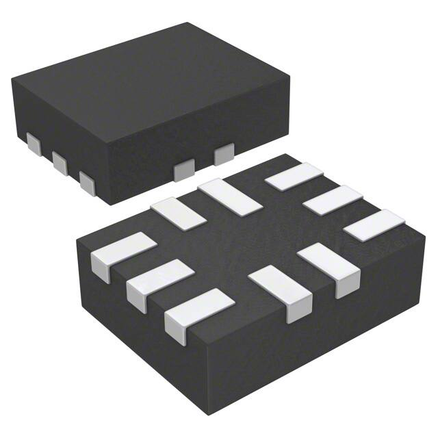
• Lead (Pb)-free low profile miniQFN-10 (1.4 mm x 1.8 mm
x 0.55 mm)
Key applications for the DG9636 are logic level translation,
pulse generator, and high speed or low noise signal
switching in precision instrumentations and portable device
designs.
• Material categorization: For definitions of compliance
please see www.vishay.com/doc?99912
The DG9636 is available in space saving 1.4 mm x 1.8 mm
miniQFN10 package.
APPLICATIONS
As a committed partner to the community and the
environment, Vishay Siliconix manufactures this product
with lead (Pb)-free device termination. The miniQFN-10
package has a nickel-palladium-gold device termination
and is represented by the lead (Pb)-free “-E4” suffix to the
ordering part number. The nickel-palladium-gold device
terminations meet all JEDEC® standards for reflow and MSL
rating.
• High-end data acquisition
• Medical instruments
• Precision instruments
• High speed communications applications
• Automated test equipment
• Sample and hold applications
FUNCTIONAL BLOCK DIAGRAM AND PIN CONFIGURATION
DG9636
miniQFN - 10L
S2A
7
S2B
6
V+ 8
A1 9
5 D2
4 D1
Logic
3 S1B
A0 10
1
Pin 1: LONG LEAD
2
GND S1A
Top View
Yx
Pin 1
Device marking: Yx for DG9636
x = Date/Lot Traceability Code
TRUTH TABLE
Selected Input
On Switches
A1
A0
DG9636
X
0
D1 to S1A
X
1
D1 to S1B
0
X
D2 to S2A
1
X
D2 to S2B
S14-0483-Rev. C, 10-Mar-14
Document Number: 65159
1
For technical questions, contact: analogswitchtechsupport@vishay.com
THIS DOCUMENT IS SUBJECT TO CHANGE WITHOUT NOTICE. THE PRODUCTS DESCRIBED HEREIN AND THIS DOCUMENT
ARE SUBJECT TO SPECIFIC DISCLAIMERS, SET FORTH AT www.vishay.com/doc?91000
�DG9636
www.vishay.com
Vishay Siliconix
ORDERING INFORMATION
Temp. Range
Package
Part Number
-40 °C to 125 °C
10 pin miniQFN
DG9636EN-T1-E4
-40 °C to 85 °C
10 pin miniQFN
DG9636DN-T1-E4
Note
• -40 °C to 85 °C datasheet limits apply.
ABSOLUTE MAXIMUM RATINGS (TA = 25 °C, unless otherwise noted)
Parameter
Limit
V+ to GND
Digital Inputs
Unit
14
a,
VS, VD
V
(V+) +0.3 or 30 mA, whichever occurs first
Continuous Current (Any Terminal)
30
Peak Current, S or D (Pulsed 1 ms, 10 % Duty Cycle)
100
Storage Temperature
mA
-65 to 150
°C
Power Dissipation (Package) b
10 pin miniQFN c, d
208
mW
Thermal Resistance (Package) b
10 pin miniQFN
357
°C/W
Notes
a. Signals on SX, DX, or AX exceeding V+ or V- will be clamped by internal diodes. Limit forward diode current to maximum current ratings.
b. All leads welded or soldered to PC board.
c. Derate 2.6 mW/°C above 70 °C.
d. Manual soldering with iron is not recommended for leadless components. The miniQFN-10 is a leadless package. The end of the lead
terminal is exposed copper (not plated) as a result of the singulation process in manufacturing. A solder fillet at the exposed copper lip
cannot be guaranteed and is not required to ensure adequate bottom side solder interconnection.
SPECIFICATIONS
Parameter
Symbol
Test Conditions
Unless Otherwise Specified
Temp. b
V+ = 12 V, VA0, A1 = 1.65 V, 0.5 V a
-40 °C to 125 °C -40 °C to 85 °C
Typ. c
Min. d
Max. d
Min. d
Max. d
Unit
Analog Switch
Analog Signal Range e
On-Resistance
On-Resistance Match
On-Resistance Flatness
VANALOG
RDS(on)
Ron
IS = 1 mA, VD = +11.3 V
IS = 1 mA, VD = +11.3 V
RFLATNESS IS = 1 mA, VD = 0.7 V, 6.5 V, 11.3 V
IS(off)
Switch Off
Leakage Current
V+ = 12 V,
VD = 1 V/11 V, VS = 11 V/1 V
ID(off)
Full
-
-
12
-
12
Room
83
-
110
-
110
Full
-
-
140
-
125
Room
2
-
4
-
4
Full
-
-
9
-
6
Room
33
-
45
-
45
Full
-
-
55
-
50
Room
± 0.01
-1
1
-1
1
Full
-
-18
18
-2
2
Room
± 0.01
-1
1
-1
1
Full
-
-18
18
-2
2
ID(on)
V+ = 12 V,
VD = VS 11 V/1 V
Room
± 0.01
-1
1
-1
1
Full
-
-18
18
-2
2
Input Current, VIN Low
IIL
VAX = 0.5 V
Full
0.005
-0.1
0.1
-0.1
0.1
Input Current, VIN High
IIH
VAX = 1.65 V
Full
0.005
-0.1
0.1
-0.1
0.1
Input Capacitance e
CIN
f = 1 MHz
Room
3
-
-
-
-
Channel On
Leakage Current
V
nA
Digital Control
S14-0483-Rev. C, 10-Mar-14
μA
pF
Document Number: 65159
2
For technical questions, contact: analogswitchtechsupport@vishay.com
THIS DOCUMENT IS SUBJECT TO CHANGE WITHOUT NOTICE. THE PRODUCTS DESCRIBED HEREIN AND THIS DOCUMENT
ARE SUBJECT TO SPECIFIC DISCLAIMERS, SET FORTH AT www.vishay.com/doc?91000
�DG9636
www.vishay.com
Vishay Siliconix
SPECIFICATIONS
Parameter
Symbol
Test Conditions
Unless Otherwise Specified
Temp. b
V+ = 12 V, VA0, A1 = 1.65 V, 0.5 V a
-40 °C to 125 °C -40 °C to 85 °C
Typ. c
Min. d
Max. d
Min. d
Max. d
Unit
Dynamic Characteristics
Turn-On Time
ton
Turn-Off Time
toff
RL = 300, CL = 35 pF
see figure 1, 2
Room
30
-
70
-
70
Full
-
-
90
-
80
Room
15
-
55
-
55
Full
-
-
75
-
65
Room
15
5
-
5
-
Full
-
2
-
2
-
23.5
-
-
-
-
ns
Break-Before-Make
tBBM
Charge Injection e
QINJ
Vg = 0 V, Rg = 0 , CL = 1 nF
Room
OIRR
RL = 50 , CL = 5 pF, f = 10 MHz
Room
-58
-
-
-
-
dB
BW
RL = 50
Room
720
-
-
-
-
MHz
XTALK
RL = 50 , CL = 5 pF, f = 10 MHz
Room
-67
-
-
-
-
dB
Room
2
-
-
-
-
Room
7.7
-
-
-
-
Room
0.01
-
-
-
-
Room
0.001
-
0.5
-
0.5
Full
-
-
1
-
1
Room
-0.001
-0.5
-
-0.5
-
Full
-
-1
-
-1
-
Temp. b
Typ. c
Off Isolation
e
Bandwidth e
Channel-to-Channel
Crosstalk e
pC
Dynamic Characteristics
Source Off
Capacitance e
CS(off)
Channel On
Capacitance e
CD(on)
Total Harmonic
Distortion e
THD
f = 1 MHz
Signal = 1 VRMS, 20 Hz to 20 kHz,
RL = 600
pF
%
Power Supplies
Power Supply Current
I+
VIN = 0 V, or V+
Ground Current
IGND
μA
SPECIFICATIONS
Parameter
Symbol
Test Conditions
Unless Otherwise Specified
V+ = 5 V, VA0, A1 = 1.4 V, 0.5 V a
-40 °C to 125 °C -40 °C to 85 °C
Min. d
Max. d
Min. d
Max. d
Unit
Analog Switch
Analog Signal Range e
On-Resistance
VANALOG
RDS(on)
IS = 1 mA, VD = +3.5 V
On-Resistance Match
Switch Off
Leakage Current
Ron
IS(off)
ID(off)
Channel On
Leakage Current
V+ = 5.5 V,
VD = 1 V/4.5 V, VS = 4.5 V/1 V
Full
-
-
5
-
5
Room
120
-
170
-
170
Full
-
-
250
-
200
Room
3
-
5
-
5
Full
-
-
12
-
10
Room
± 0.01
-1
1
-1
1
Full
-
-18
18
-2
2
Room
± 0.01
-1
1
-1
1
Full
-
-18
18
-2
2
Room
± 0.01
-1
1
-1
1
Full
-
-18
18
-2
2
ID(on)
V+ = 5.5 V, VS = VD = 1 V/4.5 V
Input Current, VIN Low
IL
VAX = 0.5 V
Full
0.005
-0.1
0.1
-0.1
0.1
Input Current, VIN High
IH
VAX = 1.4 V
Full
0.005
-0.1
0.1
-0.1
0.1
CIN
f = 1 MHz
Room
3
-
-
-
-
V
nA
Digital Control
Input Capacitance
S14-0483-Rev. C, 10-Mar-14
μA
pF
Document Number: 65159
3
For technical questions, contact: analogswitchtechsupport@vishay.com
THIS DOCUMENT IS SUBJECT TO CHANGE WITHOUT NOTICE. THE PRODUCTS DESCRIBED HEREIN AND THIS DOCUMENT
ARE SUBJECT TO SPECIFIC DISCLAIMERS, SET FORTH AT www.vishay.com/doc?91000
�DG9636
www.vishay.com
Vishay Siliconix
SPECIFICATIONS
Parameter
Symbol
Test Conditions
Unless Otherwise Specified
V+ = 5 V, VA0, A1 = 1.4 V, 0.5 V a
-40 °C to 125 °C -40 °C to 85 °C
Temp. b
Typ. c
Room
Min. d
Max. d
Min. d
Max. d
55
-
-
-
-
Full
-
-
-
-
-
Room
30
-
-
-
-
Full
-
-
-
-
-
Room
36
-
-
-
-
Full
-
-
-
-
-
Full
10
-
-
-
-
Room
-58
-
-
-
-
Room
-68
-
-
-
-
Unit
Dynamic Characteristics
Turn-On Time
ton
Turn-Off Time
toff
Break-Before-Make-Time
Charge Injection
Off-Isolation
e
e
RL = 300 , CL = 35 pF
see figure 1, 2
tBMM
QINJ
OIRR
CL = 1 nF, RGEN = 0 , VGEN = 0 V
f = 10 MHz, RL = 50 , CL = 5 pF
ns
pC
dB
Crosstalk e
XTALK
Bandwidth e
BW
RL = 50
Room
610
-
-
-
-
MHz
Total Harmonic
Distortion e
THD
Signal = 1 VRMS, 20 Hz to 20 kHz,
RL = 600
Room
2.2
-
-
-
-
%
Source Off Capacitance e
CS(off)
2.1
-
-
-
-
f = 1 MHz
Room
8.1
-
-
-
-
Room
0.001
-
0.5
-
0.5
Full
-
-
1
-
1
Room
-0.001
-0.5
-
-0.5
-
Full
-
-1
-
-1
-
Temp.b
Typ. c
Full
-
-
Room
200
Channel On
Capacitance e
CD(on)
pF
Power Supplies
Power Supply Current
I+
VIN = 0 V, or V+
Ground Current
IGND
μA
SPECIFICATIONS
Parameter
Symbol
Test Conditions
Unless Otherwise Specified
V+ = 3 V, VA0, A1 = 1.4 V, 0.5 V a
-40 °C to 125 °C
Max. d
3
-
3
-
245
-
245
Max.
d
-40 °C to 85 °C
Min. d
Min.
d
Unit
Analog Switch
Analog Signal Range e
On-Resistance
VANALOG
RDS(on)
IS = 1 mA, VD = +1.5 V
On-Resistance Match
Switch Off
Leakage Current
(for 16 pin miniQFN)
Channel On
Leakage Current
(for 16 pin miniQFN)
Ron
IS(off)
V+ = 3.3 V, V- = 0 V
VD = 1 V/3 V, VS = 3 V/1 V
ID(off)
Full
-
-
325
-
290
Room
5
-
6
-
6
Full
-
-
13
-
11
Room
± 0.01
-1
1
-1
1
Full
-
-18
18
-2
2
Room
± 0.01
-1
1
-1
1
Full
-
-18
18
-2
2
Room
± 0.01
-1
1
-1
1
Full
-
-18
18
-2
2
ID(on)
V+ = 3.3 V, V- = 0 V,
VS = VD = 1 V/3 V
Input Current, VIN Low
IL
VAX = 0.5 V
Full
0.005
-0.1
0.1
-0.1
0.1
Input Current, VIN High
IH
VAX = 1.4 V
Full
0.005
-0.1
0.1
-0.1
0.1
CIN
f = 1 MHz
Room
3.1
-
-
-
-
V
nA
Digital Control
Input Capacitance
S14-0483-Rev. C, 10-Mar-14
μA
pF
Document Number: 65159
4
For technical questions, contact: analogswitchtechsupport@vishay.com
THIS DOCUMENT IS SUBJECT TO CHANGE WITHOUT NOTICE. THE PRODUCTS DESCRIBED HEREIN AND THIS DOCUMENT
ARE SUBJECT TO SPECIFIC DISCLAIMERS, SET FORTH AT www.vishay.com/doc?91000
�DG9636
www.vishay.com
Vishay Siliconix
SPECIFICATIONS
Parameter
Symbol
Test Conditions
Unless Otherwise Specified
V+ = 3 V, VA0, A1 = 1.4 V, 0.5 V a
-40 °C to 125 °C
-40 °C to 85 °C
Temp.b
Typ. c
Room
96
-
-
-
-
Full
-
-
-
-
-
Room
60
-
-
-
-
Full
-
-
-
-
-
Room
77
-
-
-
-
Full
-
-
-
-
-
Min.
d
Max.
d
Min. d
Max. d
Unit
Dynamic Characteristics
Enable Turn-On Time
ton
Enable Turn-Off Time
toff
Break-Before-Make-Time
Charge
Injection e
tBMM
QINJ
Off-Isolation e
OIRR
Crosstalk e
XTALK
Bandwidth e
BW
Total Harmonic
Distortion e
THD
Source Off Capacitance e
CS(off)
Channel On
Capacitance e
RL = 300 , CL = 35 pF
see figure 1, 2
CD(on)
CL = 1 nF, RGEN = 0 , VGEN = 0 V
ns
Full
6.6
-
-
-
-
Room
-57
-
-
-
-
Room
-69
-
-
-
-
RL = 50
Room
525
-
-
-
-
MHz
Signal = 1 VRMS, 20 Hz to 20 kHz,
RL = 600
Room
2.2
-
-
-
-
%
2.1
-
-
-
-
f = 1 MHz
Room
8.3
-
-
-
-
0.001
-
0.5
-
0.5
f = 10 MHz, RL = 50 , CL = 5 pF
pC
dB
pF
Power Supplies
Power Supply Current
Room
I+
VIN = 0 V, or V+
Ground Current
IGND
Full
-
-
1
-
1
Room
-0.001
-0.5
-
-0.5
-
Full
-
-1
-
-1
-
μA
Notes
a. VIN = input voltage to perform proper function.
b. Room = 25 ºC, Full = as determined by the operating temperature.
c. Typical value are for DESIGN AID ONLY, not guaranteed nor subject to production testing.
d. The algebraic convention whereby the most negative value is a minimum and the most positive a maximum, is used in this datasheet.
e. Guaranteed by design, not subject to production test.
Stresses beyond those listed under “Absolute Maximum Ratings” may cause permanent damage to the device. These are stress ratings only, and functional operation
of the device at these or any other conditions beyond those indicated in the operational sections of the specifications is not implied. Exposure to absolute maximum
rating conditions for extended periods may affect device reliability.
S14-0483-Rev. C, 10-Mar-14
Document Number: 65159
5
For technical questions, contact: analogswitchtechsupport@vishay.com
THIS DOCUMENT IS SUBJECT TO CHANGE WITHOUT NOTICE. THE PRODUCTS DESCRIBED HEREIN AND THIS DOCUMENT
ARE SUBJECT TO SPECIFIC DISCLAIMERS, SET FORTH AT www.vishay.com/doc?91000
�DG9636
www.vishay.com
Vishay Siliconix
TYPICAL CHARACTERISTICS (25 °C, unless otherwise noted)
500
350
T = 25 °C
IS = 1 mA
VCC = 2.7 V
300
+ 85 °C
+ 25 °C
+ 125 °C
- 40 °C
400
RON - On-Resistance ()
VCC = 3.0 V
RON - On-Resistance ()
V+ = 3.0 V
IS = 1 mA
450
250
200
VCC = 5.0 V
150
VCC = 12.0 V
100
VCC = 10.8 V
350
300
250
200
150
100
50
50
VCC = 13.2 V
0
0
0
2
4
6
8
10
12
14
0
1
1.5
2
2.5
3
VD - Analog Voltage (V)
On-Resistance vs. Single Supply Voltage
On-Resistance vs. Analog Voltage and Temperature
350
150
V + = 12.0 V
IS = 1m A
V+ = 5.0 V
IS = 1 mA
125
+ 125 °C
+ 85 °C
+ 25 °C
- 40 °C
250
RON - On-Resistance ()
300
RON - On-Resistance ()
0.5
VD - Analog Voltage (V)
200
150
100
+ 25 °C
+ 85 °C
+ 125 °C
100
- 40 °C
75
50
25
50
0
0
0
0.5
1
1.5
2
2.5
3
3.5
4
4.5
5
0
1
2
3
4
5
6
7
8
9
10
11
12
VD - Analog Voltage (V)
VD - Analog Voltage (V)
On-Resistance vs. Analog Voltage and Temperature
On-Resistance vs. Analog Voltage and Temperature
100 µA
10 000
V+ = +12.0 V
V+ = 13.2 V
1000
1 µA
Leakage Current (pA)
Supply Current (A)
10 µA
100 nA
IGND
I+
1 nA
100 pA
ID(off)
100
IS(off)
ID(on)
10
10 pA
1 pA
10
100
1K
10K
100K
1M
10M
Input Switching Frequency (Hz)
Supply Current vs. Input Switching Frequency
S14-0483-Rev. C, 10-Mar-14
1
- 60 - 40 - 20
0
20
40
60
80
100 120 140
Temperature (°C)
Leakage Current vs. Temperature
Document Number: 65159
6
For technical questions, contact: analogswitchtechsupport@vishay.com
THIS DOCUMENT IS SUBJECT TO CHANGE WITHOUT NOTICE. THE PRODUCTS DESCRIBED HEREIN AND THIS DOCUMENT
ARE SUBJECT TO SPECIFIC DISCLAIMERS, SET FORTH AT www.vishay.com/doc?91000
�DG9636
www.vishay.com
Vishay Siliconix
TYPICAL CHARACTERISTICS (25 °C, unless otherwise noted)
25
0
LOSS
- 10
15
Q - Charge Injection (pC)
LOSS, OIRR, XTALK (dB)
- 20
- 30
- 40
- 50
- 60
XTALK
OIRR
- 70
V+ = 12.0 V
10
5
0
-5
V+ = 3.0 V
- 10
V+ = 5.0 V
- 80
- 15
- 90
- 20
- 100
100K
T = 25 °C
CL = 1 nF
20
V+ = 12.0 V
RL = 50
- 25
1M
10M
100M
0
1G
1
2
3
4
5
6
7
8
9
10
Frequency (Hz)
VS - Analog Voltage (V)
Insertion Loss, Off-Isolation,
Crosstalk vs. Frequency
Charge Injection vs. Analog voltage
11
12
1.4
Vth - Switching Threshold (V)
1.3
1.2
VIH
1.1
1.0
0.9
VIL
0.8
0.7
0.6
0.5
0.4
2
3
4
5
6
7
8
9
10 11 12 13 14 15
V+ - Supply Voltage (V)
Switching Threshold vs. Supply Voltage
S14-0483-Rev. C, 10-Mar-14
Document Number: 65159
7
For technical questions, contact: analogswitchtechsupport@vishay.com
THIS DOCUMENT IS SUBJECT TO CHANGE WITHOUT NOTICE. THE PRODUCTS DESCRIBED HEREIN AND THIS DOCUMENT
ARE SUBJECT TO SPECIFIC DISCLAIMERS, SET FORTH AT www.vishay.com/doc?91000
�DG9636
www.vishay.com
Vishay Siliconix
TEST CIRCUITS
V+
A0 or A1
V+
S1A or S2A
50 Ω
t r < 5 ns
t f < 5 ns
VCC
V+
50 %
VAX
0V
S1B or S2B
VS1A or VS2A
D1 or D2
GND
300 Ω
90 %
90 %
VO
VO
50 %
35 pF
0V
t OFF
t ON
S1A or S2A ON
Figure 1. Enable Switching Time
V+
tr < 5 ns
tf < 5 ns
VCC
V+
SxA - SxB
A0
50 Ω
V+
50 %
VA0,A1
0V
A1
VSxA or VSxB
80 %
VO
D1 or D2
GND
VO
300 Ω
35 pF
0V
tD
Figure 2. Break-Before-Make
V+
t r < 5 ns
t f < 5 ns
V+
VCC
A0 or A1
VAX
OFF
ON
OFF
0V
Rg
SxA or SxB
VO
Vg
GND
ΔVO
VO
D1 or D2
CL
1 nF
Charge Injection = ΔVO X CL
Figure 3. Charge Injection
S14-0483-Rev. C, 10-Mar-14
Document Number: 65159
8
For technical questions, contact: analogswitchtechsupport@vishay.com
THIS DOCUMENT IS SUBJECT TO CHANGE WITHOUT NOTICE. THE PRODUCTS DESCRIBED HEREIN AND THIS DOCUMENT
ARE SUBJECT TO SPECIFIC DISCLAIMERS, SET FORTH AT www.vishay.com/doc?91000
�DG9636
www.vishay.com
Vishay Siliconix
TEST CIRCUITS
V+
V+
Network Analyzer
V+
V+
A0 or A1
Network Analyzer
V+
VIN
A0
S1A or S2A
Rg = 50 Ω
Vg
VIN
SxA or SxB
A1
Vg
VOUT
VOUT
D1 or D2
D1 or D2
GND
50 Ω
Insertion Loss = 20 log
Rg = 50 Ω
GND
50 Ω
VOUT
Off Isolation = 20 log
VIN
Figure 4. Insertion Loss
VOUT
VIN
Figure 5. Off-Isolation
V+
V+
Network Analyzer
V+
A0 or A1
V+
S1A or S2A
VIN
Vg
Rg = 50
V+
V+
A0 or A1
D1 or D2
VOUT
S1A or S2A
|
to
|
S2A or S2B
S1B or S2B
50 Ω
GND
D1 or D2
50 Ω
GND
Cross Talk = 20 log
VOUT
VIN
Figure 6. Crosstalk
Impedance
Analyzer
V-
V-
Figure 7. Source/Drain Capacitance
Vishay Siliconix maintains worldwide manufacturing capability. Products may be manufactured at one of several qualified locations. Reliability data for Silicon
Technology and Package Reliability represent a composite of all qualified locations. For related documents such as package/tape drawings, part marking, and
reliability data, see www.vishay.com/ppg?65159.
S14-0483-Rev. C, 10-Mar-14
Document Number: 65159
9
For technical questions, contact: analogswitchtechsupport@vishay.com
THIS DOCUMENT IS SUBJECT TO CHANGE WITHOUT NOTICE. THE PRODUCTS DESCRIBED HEREIN AND THIS DOCUMENT
ARE SUBJECT TO SPECIFIC DISCLAIMERS, SET FORTH AT www.vishay.com/doc?91000
�Package Information
www.vishay.com
Vishay Siliconix
MINI QFN-10L CASE OUTLINE
DIM
MILLIMETERS
INCHES
MIN.
NAM.
MAX.
MIN.
NAM.
MAX.
A
0.45
0.55
0.60
0.0177
0.0217
0.0236
A1
0.00
-
0.05
0.000
-
0.002
b
0.15
0.20
0.25
0.006
0.008
0.010
0.150 or 0.127 REF (1)
c
0.006 or 0.005 REF (1)
D
1.70
1.80
1.90
0.067
0.071
0.075
E
1.30
1.40
1.50
0.051
0.055
0.059
e
0.40 BSC
0.016 BSC
L
0.35
0.40
0.45
0.014
0.016
0.018
L1
0.45
0.50
0.55
0.0177
0.0197
0.0217
Note
(1) The dimension depends on the leadframe that assembly house used.
ECN T16-0163-Rev. B, 16-May-16
DWG: 5957
Revision: 16-May-16
1
Document Number: 74496
THIS DOCUMENT IS SUBJECT TO CHANGE WITHOUT NOTICE. THE PRODUCTS DESCRIBED HEREIN AND THIS DOCUMENT
ARE SUBJECT TO SPECIFIC DISCLAIMERS, SET FORTH AT www.vishay.com/doc?91000
�PAD Pattern
Vishay Siliconix
RECOMMENDED MINIMUM PADS FOR MINI QFN 10L
1.700
(0.0669)
9x
0.563
(0.0221)
0.663
(0.0261)
0.200
(0.0079)
1
2.100
(0.0827)
0.400
(0.0157)
Pitch
10 x
0.225
(0.0089)
Mounting Footprint
Dimensions in mm (inch)
Document Number: 66554
Revision: 05-Mar-10
www.vishay.com
1
�Legal Disclaimer Notice
www.vishay.com
Vishay
Disclaimer
ALL PRODUCT, PRODUCT SPECIFICATIONS AND DATA ARE SUBJECT TO CHANGE WITHOUT NOTICE TO IMPROVE
RELIABILITY, FUNCTION OR DESIGN OR OTHERWISE.
Vishay Intertechnology, Inc., its affiliates, agents, and employees, and all persons acting on its or their behalf (collectively,
“Vishay”), disclaim any and all liability for any errors, inaccuracies or incompleteness contained in any datasheet or in any other
disclosure relating to any product.
Vishay makes no warranty, representation or guarantee regarding the suitability of the products for any particular purpose or
the continuing production of any product. To the maximum extent permitted by applicable law, Vishay disclaims (i) any and all
liability arising out of the application or use of any product, (ii) any and all liability, including without limitation special,
consequential or incidental damages, and (iii) any and all implied warranties, including warranties of fitness for particular
purpose, non-infringement and merchantability.
Statements regarding the suitability of products for certain types of applications are based on Vishay’s knowledge of
typical requirements that are often placed on Vishay products in generic applications. Such statements are not binding
statements about the suitability of products for a particular application. It is the customer’s responsibility to validate that a
particular product with the properties described in the product specification is suitable for use in a particular application.
Parameters provided in datasheets and / or specifications may vary in different applications and performance may vary over
time. All operating parameters, including typical parameters, must be validated for each customer application by the customer’s
technical experts. Product specifications do not expand or otherwise modify Vishay’s terms and conditions of purchase,
including but not limited to the warranty expressed therein.
Except as expressly indicated in writing, Vishay products are not designed for use in medical, life-saving, or life-sustaining
applications or for any other application in which the failure of the Vishay product could result in personal injury or death.
Customers using or selling Vishay products not expressly indicated for use in such applications do so at their own risk.
Please contact authorized Vishay personnel to obtain written terms and conditions regarding products designed for
such applications.
No license, express or implied, by estoppel or otherwise, to any intellectual property rights is granted by this document
or by any conduct of Vishay. Product names and markings noted herein may be trademarks of their respective owners.
© 2017 VISHAY INTERTECHNOLOGY, INC. ALL RIGHTS RESERVED
Revision: 08-Feb-17
1
Document Number: 91000
�


 工商网监
湘ICP备2023018690号
工商网监
湘ICP备2023018690号
