Product is End of Life 12/2014
SiP4280
Vishay Siliconix
Slew Rate Controlled Load Switch
FEATURES
• 1.8 V to 5.5 V Input Voltage range
• Very Low RDS(ON), typically 80 mΩ (5 V)
• Slew rate limited turn-on time options
- SiP4280-1: 1 ms
- SiP4280-3: 100 µs
• Fast shutdown load discharge option
• Low quiescent current
• 4 kV ESD Rating
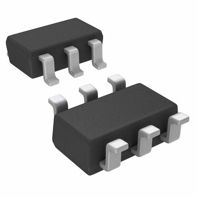
• 6 pin SOT23 package
APPLICATIONS
• Cellular telephones
• Digital still cameras
• Personal digital assistants (PDA)
• Hot swap supplies
• Notebook computers
• Personal communication devices
DESCRIPTION
The SiP4280 is a P-Channel MOSFET power switch
designed for high-side load switching applications.
The output pass transistor is a P-Channel MOSFET
transistor with typically 80 mΩ RDS(ON). The SiP4280
is available in two different versions of turn-on times.
The SiP4280-1 version has a slew rate limited turn-on
time typically of 1 ms. The SiP4280-3 version has a
slew rate limited turn-on time typically of 100 µs and
additionally offers a shutdown load discharge circuit to
rapidly turn off a load circuit when the switch is disabled.
Both SiP4280 load switch versions operate with an
input voltage ranging from 1.8 V to 5.5 V, making them
ideal for both 3 V and 5 V applications. The SiP4280
also features an under-voltage lock out which turns
the switch off when an input undervoltage condition
exists. Input logic levels are TTL and 2.5 V to 5.0 V
CMOS compatible. The quiescent supply current is
very low, typically 2.5 µA. In shutdown mode, the supply current decreases to less than 1.0 µA.
The SiP4280 is available in a 6 pin SOT23 package
and is specified over - 40 °C to 85 °C temperature
range.
TYPICAL APPLICATION CIRCUIT
VIN
VIN
VOUT
OUT
CIN
1 µF
COUT
0.1 µF
ON
ON/OFF
GND
GND
Document Number: 73476
S-61690–Rev. D, 04-Sep-06
GND
www.vishay.com
1
�SiP4280
Vishay Siliconix
ABSOLUTE MAXIMUM RATINGS
Parameter
Supply Input Voltage
Enable Input Voltage
Output Voltage
Maximum Switch Current
Maximum Pulsed Current
VIN ≥ 2.5
VIN < 2.5
Junction Temperature
Thermal Resistance
SOT23-6L
Power Dissipation
SOT23-6Lb
Notes:
a. Device mounted with all leads soldered or welded to PC board.
b. Derate 5.5 mW/°C above TA = 70 °C.
Symbol
Steady State
Unit
VIN
VON
VOUT
IMAX
IDM
IDM
TJ
- 0.3 to 6
- 0.3 to 6
- 0.3 to VIN + 0.3
V
2.3
6
3
A
- 40 to 150
180
440
°C
°C/W
mW
ΦJAa
PD
Stresses beyond those listed under "Absolute Maximum Ratings" may cause permanent damage to the device. These are stress ratings only,
and functional operation of the device at these or any other conditions beyond those indicated in the operational sections of the specifications is
not implied. Exposure to absolute maximum rating/conditions for extended periods may affect device reliability.
RECOMMENDED OPERATING RANGE all voltages referenced to GND = 0 V
Parameter
Symbol
VIN
Operating Temperature Range
Steady State
1.8 to 5.5
- 40 to 85
Unit
V
°C
SPECIFICATIONS
Parameter
SiP4280 All Versions
Operating Voltagec
Undervoltage Lockout
Undervoltage Lockout Hysteresis
Quiescent Current
Off Supply Current
Off Switch Current
Typb
Maxa
ISINK
VIN = 2.7 V to 5.5 V
VIN = 2.7 V to ≤ 4.2 V
VIN > 4.2 V to 5.5 V
VON/OFF = 5.5 V
1.8
1.0
2
2.4
-
1.4
250
2.5
0.01
0.01
80
85
100
160
2800
-
5.5
1.8
4
1
1
120
130
150
250
0.8
1
TD(ON)
TON
TD(OFF)
VIN = 5 V, RLOAD = 10 Ω, TA = 25 °C
VIN = 5 V, RLOAD = 10 Ω, TA = 25 °C
VIN = 5 V, RLOAD = 10 Ω, TA = 25 °C
-
20
1000
4
40
1500
10
TD(ON)
TON
TD(OFF)
RPD
VIN = 5 V, RLOAD = 10 Ω, TA = 25 °C
VIN = 5 V, RLOAD = 10 Ω, TA = 25 °C
VIN = 5 V, RLOAD = 10 Ω, TA = 25 °C
ON/OFF = inactive, TA = 25 °C
-
20
100
4
150
40
150
10
250
Symbol
VIN
VUVLO
VUVLO(hyh)
IQ
IQ(OFF)
ISD(OFF)
RDS(ON)
On-Resistance Temp-Coefficient
ON/OFF Input Low Voltaged
TCRDS
VIL
ON/OFF Input Leakage
SiP4280-1 Version
Output Turn-On Delay Time
Output Turn-On Rise Time
Output Turn-Off Delay Time
SiP4280-3 Version
Output Turn-On Delay Time
Output Turn-On Rise Time
Output Turn-Off Delay Time
Output Pull-Down Resistance
Limits
Mina
On-Resistance
ON/OFF Input High Voltage
Test Conditions Unless Specified
VIN = 5 V, TA = - 40 to + 85 °C
VIH
VIN Falling
ON/OFF = active
ON/OFF = inactive, OUT = open
ON/OFF = inactive, VOUT = 0
VIN = 5 V, TA = 25 °C
VIN = 4.2 V, TA = 25 °C
VIN = 3 V, TA = 25 °C
VIN = 1.8 V, TA = 25 °C
Unit
V
mV
µA
mΩ
ppm/°C
V
µA
µS
µS
Ω
Notes:
a. The algebraic convention whereby the most negative value is a minimum and the most positive a maximum.
b. Typical values are for DESIGN AID ONLY, not guaranteed nor subject to production testing.
c. Part requires minimum start-up of VIN ≥ 2.0 to ensure operation down to 1.8 V.
d. For VIN ≤ 2.7 V see typical ON/OFF threshold curve.
www.vishay.com
2
Document Number: 73476
S-61690–Rev. D, 04-Sep-06
�SiP4280
Vishay Siliconix
PIN CONFIGURATION
SOT23-6
Top View
O
OUT
1
6
VIN
GND
2
5
GND
ON/OFF
3
4
VIN
PIN DESCRIPTION
Pin Number Pin Name
SOT23-6
4, 6
3
2, 5
1
VIN
ON/OFF
GND
OUT
Symbol
This pin is the P-channel MOSFET source connection
Logic high enables the IC; logic low disables the IC and reduces the IC and reduces the quiescent current to 2.5 µA
Ground connection
This pin is the P-channel MOSFET drain connection
SELECTION GUIDE
Part Number
Slew Rate
(typ)
Active
Pull Down
Enable
SiP4280-1-T1-E3
SiP4280-3-T1-E3
1 ms
100 µs
No
Yes
Active High
Active High
Part Number
Marking
Temperature Range
Package
SiP4280DT-1-T1-E3
SiP4280DT-3-T1-E3
L1XXX
L3XXX
- 40 °C to 85 °C
SOT23-6L
SOT23-6L
ORDERING INFORMATION
Document Number: 73476
S-61690–Rev. D, 04-Sep-06
www.vishay.com
3
�SiP4280
Vishay Siliconix
TYPICAL CHARACTERISTICS internally regulated, 25 °C unless noted
4.0
3.5
3.5
3.0
3.0
Quiescent Current (µA)
V=5V
IQ (µA)
2.5
2.0
VIN = 3 V
1.5
1.0
2.5
2.0
1.5
1.0
0.5
0.5
0.0
- 40
0.0
- 25
0
25
50
75
85
0
1
2
3
4
5
6
VIN (V)
Temperature (°C)
Quiescent Current vs. Temperature
Quiescent Current vs. Input Voltage
250
140
230
130
2A
210
120
V=3V
1A
rDS(ON) (mΩ)
rDS(ON) (mΩ)
190
170
500 mA
150
130
110
V=5V
100
90
110
90
80
100 mA
70
70
50
1.5
2.0
2.5
3.0
3.5
4.0
4.5
5.0
60
- 40
5.5
- 25
VIN (V)
1.6
2.0
1.4
1.8
75
85
75
100
85
1.2
1.6
IoffSW (µA)
ON/OFF Threshold (V)
50
RDS(ON) vs. Temperature
2.2
1.4
1.2
VIH
VIL
1.0
1.0
0.8
0.6
0.4
0.8
0.2
0.6
2.0
2.5
3.0
3.5
4.0
4.5
5.0
VIN (V)
ON/OFF Threhold vs. Input Voltage
www.vishay.com
4
25
Temperature (°C)
RDS(ON) vs. Input Voltage
0.4
1.5
0
5.5
0.0
- 40
- 25
0
25
50
Temperature (°C)
Off Switch Current vs. Temperature
Document Number: 73476
S-61690–Rev. D, 04-Sep-06
�SiP4280
Vishay Siliconix
TYPICAL WAVEFORMS
ON/OFF (5 V/div.)
ON/OFF (5 V/div.)
VOUT (2 V/div.)
VOUT (2 V/div.)
IIN (200 mA/div.)
IIN (200 mA/div.)
Time (500 µs/div)
SiP4280-1 Turn-On (VIN = 3 V, RLOAD = 6 Ω)
Time (5 µs/div)
SiP4280-1 Turn-Off (VIN = 3 V, RLOAD = 6 Ω)
ON/OFF (5 V/div.)
ON/OFF (5 V/div.)
VOUT (2 V/div.)
VOUT (2 V/div.)
IIN (200 mA/div.)
IIN (200 mA/div.)
Time (500 µs/div)
SiP4280-1 Turn-On (VIN = 5 V, RLOAD = 10 Ω)
Document Number: 73476
S-61690–Rev. D, 04-Sep-06
Time (5 µs/div)
SiP4280-1 Turn-Off (VIN = 5 V, RLOAD = 10 Ω)
www.vishay.com
5
�SiP4280
Vishay Siliconix
TYPICAL WAVEFORMS
ON/OFF (5 V/div.)
ON/OFF (5 V/div.)
VOUT (2 V/div.)
VOUT (2 V/div.)
IIN (200 mA/div.)
IIN (200 mA/div.)
Time (50 µs/div)
Time (5 µs/div)
SiP4280-3 Turn-On (VIN = 3 V, RLOAD = 6 Ω)
SiP4280-3 Turn-Off (VIN = 3 V, RLOAD = 6 Ω)
ON/OFF (5 V/div.)
ON/OFF (5 V/div.)
VOUT (2 V/div.)
VOUT (2 V/div.)
IIN (200 mA/div.)
IIN (200 mA/div.)
Time (50 µs/div)
SiP4280-3 Turn-On (VIN = 5 V, RLOAD = 10 Ω)
www.vishay.com
6
Time (5 µs/div)
SiP4280-3 Turn-Off (VIN = 5 V, RLOAD = 10 Ω)
Document Number: 73476
S-61690–Rev. D, 04-Sep-06
�SiP4280
Vishay Siliconix
BLOCK DIAGRAM
SiP4280–3 Version only
SiP4280 Functional Block Diagramm
DETAILED DESCRIPTION
The SiP4280 is a P-Channel MOSFET power
switches designed for high-side slew rate controlled
load switching applications. Once turned on, the slewrate control circuitry is activated and current is ramped
in a linear fashion until it reaches the level required for
the output load condition. This is accomplished by first
elevating the gate voltage of the MOSFET up to its
threshold voltage and then by linearly increasing the
gate voltage until the MOSFET becomes fully
enhanced. At this point, the gate voltage is then
quickly increased to the full input voltage to reduce
RDS(ON) of the MOSFET switch and minimize any
associated power losses.
Document Number: 73476
S-61690–Rev. D, 04-Sep-06
The SiP4280-1 version has a modest 1 ms turn on
slew rate feature, which significantly reduces in-rush
current at turned on time and permits the load switch
to be implemented with a small input capacitor, or no
input capacitor at all, saving cost and space. In addition to a 100 µs minimized slew rate, the SIP4280-3
features a shutdown output discharge circuit which is
activated at shutdown (when the part is disabled
through the ON/OFF pin) and discharges the output
pin through a small internal resistor hence, turning off
the load.
In instances where the input voltage falls below 1.4 V
(typically) the under voltage lock-out circuitry protects
the MOSFET switch from entering the saturation
region or operation by shutting down the chip.
www.vishay.com
7
�SiP4280
Vishay Siliconix
APPLICATION INFORMATION
Input Capacitor
While a bypass capacitor on the input is not required, a
1 µF or larger capacitor for CIN is recommended in
almost all applications. The Bypass capacitor should be
placed as physically close as possible to the SiP4280 to
be effective in minimizing transients on the input.
Ceramic capacitors are recommended over tantalum
because of their ability to withstand input current surges
from low impedance sources such as batteries in portable devices.
Output Capacitor
A 0.1 µF capacitor or larger across VOUT and GND is
recommended to insure proper slew operation. COUT
may be increased without limit to accommodate any
load transient condition with only minimal affect on the
SiP4280 turn on slew rate time. There are no ESR or
capacitor type requirement.
Enable
The ON/OFF pin is compatible with both TTL and
CMOS logic voltage levels.
Reverse Voltage Conditions and Protection
The P-Channel MOSFET pass transistor has an intrinsic diode that is reversed biased when the input voltage
is greater than the output voltage. Should VOUT exceed
VIN , this intrinsic diode will become forward biased and
allow excessive current to flow into the IC thru the VOUT
pin and potentially damage the IC device. Therefore
extreme care should be taken to prevent VOUT from
exceeding VIN.
In conditions where VOUT exceeds VIN a Schottky diode
in parallel with the internal intrinsic diode is recommended to protect the SiP4280.
Vishay Siliconix maintains worldwide manufacturing capability. Products may be manufactured at one of several qualified locations. Reliability data for Silicon Technology and Package Reliability represent a composite of all qualified locations. For related documents such as package/tape drawings, part marking, and reliability
data, see http://www.vishay.com/ppg?73476
www.vishay.com
8
Document Number: 73476
S-61690–Rev. D, 04-Sep-06
�Package Information
www.vishay.com
Vishay Siliconix
Thin SOT-23 : 5- and 6-Lead (Power IC only)
e1
6
5
4
E1
1
2
E
3
-B-
4
Pin #1
indetifier
e
0.15 M
C B A
b
-AD
4 x θ1
0.17 ref
c
R
A2
R
L
A
Gage plane
Seating plane
θ
Seating plane
4 x θ1
A1
0.08 C
L
(L1)
-CNotes:
1. Use millimeters as the primary measurement.
2. Dimensioning and tolerances conform to ASME Y14.5M. - 1994.
3. This part is fully compliant with JEDEC MO-193.
4. Detail of Pin #1 indentifier is optional.
MILLIMETERS
INCHES
DIM.
MIN.
NOM.
MAX.
MIN.
NOM.
A
0.91
1.00
1.10
0.036
0.039
MAX.
0.043
A1
0.00
0.05
0.10
0.000
0.002
0.004
0.039
A2
0.85
0.90
1.00
0.033
0.035
b
0.30
0.40
0.45
0.012
0.016
0.018
c
0.10
0.15
0.20
0.004
0.006
0.008
D
2.85
2.95
3.10
0.112
0.116
0.122
E
2.70
2.85
2.98
0.106
0.112
0.117
E1
1.525
1.65
1.70
0.060
0.065
0.067
0.50
0.014
e
L
0.95 BSC
0.30
0.40
L1
0.60 ref.
L2
0.25 BSC
0.0374 BSC
-
0.020
0.024 BSC
0.010 BSC
0°
4°
8°
0°
4°
8°
1
4°
10°
12°
4°
10°
12°
ECN: E13-1126-Rev. B, 01-Jul-13
DWG: 5926
Revision: 01-Jul-13
Document Number: 72821
1
For technical questions, contact: powerictechsupport@vishay.com
THIS DOCUMENT IS SUBJECT TO CHANGE WITHOUT NOTICE. THE PRODUCTS DESCRIBED HEREIN AND THIS DOCUMENT
ARE SUBJECT TO SPECIFIC DISCLAIMERS, SET FORTH AT www.vishay.com/doc?91000
�Legal Disclaimer Notice
www.vishay.com
Vishay
Disclaimer
ALL PRODUCT, PRODUCT SPECIFICATIONS AND DATA ARE SUBJECT TO CHANGE WITHOUT NOTICE TO IMPROVE
RELIABILITY, FUNCTION OR DESIGN OR OTHERWISE.
Vishay Intertechnology, Inc., its affiliates, agents, and employees, and all persons acting on its or their behalf (collectively,
“Vishay”), disclaim any and all liability for any errors, inaccuracies or incompleteness contained in any datasheet or in any other
disclosure relating to any product.
Vishay makes no warranty, representation or guarantee regarding the suitability of the products for any particular purpose or
the continuing production of any product. To the maximum extent permitted by applicable law, Vishay disclaims (i) any and all
liability arising out of the application or use of any product, (ii) any and all liability, including without limitation special,
consequential or incidental damages, and (iii) any and all implied warranties, including warranties of fitness for particular
purpose, non-infringement and merchantability.
Statements regarding the suitability of products for certain types of applications are based on Vishay's knowledge of typical
requirements that are often placed on Vishay products in generic applications. Such statements are not binding statements
about the suitability of products for a particular application. It is the customer's responsibility to validate that a particular product
with the properties described in the product specification is suitable for use in a particular application. Parameters provided in
datasheets and / or specifications may vary in different applications and performance may vary over time. All operating
parameters, including typical parameters, must be validated for each customer application by the customer's technical experts.
Product specifications do not expand or otherwise modify Vishay's terms and conditions of purchase, including but not limited
to the warranty expressed therein.
Hyperlinks included in this datasheet may direct users to third-party websites. These links are provided as a convenience and
for informational purposes only. Inclusion of these hyperlinks does not constitute an endorsement or an approval by Vishay of
any of the products, services or opinions of the corporation, organization or individual associated with the third-party website.
Vishay disclaims any and all liability and bears no responsibility for the accuracy, legality or content of the third-party website
or for that of subsequent links.
Except as expressly indicated in writing, Vishay products are not designed for use in medical, life-saving, or life-sustaining
applications or for any other application in which the failure of the Vishay product could result in personal injury or death.
Customers using or selling Vishay products not expressly indicated for use in such applications do so at their own risk. Please
contact authorized Vishay personnel to obtain written terms and conditions regarding products designed for such applications.
No license, express or implied, by estoppel or otherwise, to any intellectual property rights is granted by this document or by
any conduct of Vishay. Product names and markings noted herein may be trademarks of their respective owners.
© 2022 VISHAY INTERTECHNOLOGY, INC. ALL RIGHTS RESERVED
Revision: 01-Jan-2022
1
Document Number: 91000
�


 工商网监
湘ICP备2023018690号
工商网监
湘ICP备2023018690号
